MLX90374 - Triaxis® Position Processor
Datasheet
Features and Benefits
Triaxis Hall Technology
On Chip Signal Processing for Robust
Absolute Position Sensing
ISO26262 ASIL-C Safety
Element out of Context
AEC-Q100 Qualified
Programmable Measurement Range
Programmable Linear Transfer Characteristic
(4 or 8 Multi-points or 16 or 32 PWL)
PWM Redundant Dual Output
SENT and Programmable Switch Dual Output
SAE J2716 APR2016 SENT
Enhanced serial data communication
48 bits ID Number option
Single Die - SOIC-8 Package (RoHS)
PCB-less DMP-4 Package (RoHS)
Robustness against stray-field
SOIC-8
DMP-4
Application Examples
Absolute Rotary Position Sensor
Pedal Position Sensor
Throttle Position Sensor
Ride Height Position Sensor
Absolute Linear Position Sensor
Steering Wheel Position Sensor
Float-Level Sensor
Non-Contacting Potentiometer
REVISION 4 - 20 MAR 2019
3901090374
Description
The MLX90374 is a monolithic magnetic position
processor IC. It consists of a Triaxis® Hall magnetic
front end, an analog to digital signal conditioner, a
DSP for advanced signal processing and a dual
output stage driver.
The MLX90374 is sensitive to the three
components of the magnetic flux density applied to
the IC (i.e. Bx, By and Bz). This allows the MLX90374
with the correct magnetic circuit to decode the
absolute position of any moving magnet (e.g.
rotary position from 0 to 360 Degrees or linear
displacement, see fig. 2). It enables the design of
non-contacting position sensors that are
frequently required for both automotive and
industrial applications.
The MLX90374 provides either a dual PWM output
or a combination of SENT plus a programmable
switch function. In dual PWM output mode, the
circuit offers a wide panel of configurations from
fully redundant signals to individually configurable
outputs, including the choice between several
error reporting modes. In SENT mode, the circuit
delivers enhanced serial messages consisting of
error codes, and user-defined values.
�MLX90374 - Triaxis® Position Processor
Datasheet
Ordering Information
Temp.
Package
Option Code
Packing
Form
MLX90374
G
DC
ABB-200
RE
Linear position Strayfield Immune
MLX90374
G
DC
ABB-300
RE
Angular Rotary / Linear position
MLX90374
G
VS
ABB-200
RE/RX
Linear position Strayfield Immune
MLX90374
G
VS
ABB-207
RE/RX
Linear position Strayfield Immune
MLX90374
G
VS
ABB-300
RE/RX
Angular Rotary / Linear position
MLX90374
G
VS
ABB-307
RE/RX
Angular Rotary / Linear position
MLX90374
G
DC
ABC-100
RE
Angular Rotary Strayfield Immune
MLX90374
G
DC
ABC-200
RE
Linear position Strayfield Immune
MLX90374
G
DC
ABC-300
RE
Angular Rotary / Linear position
MLX90374
G
VS
ABC-100
RE/RX
Angular Rotary Strayfield Immune
MLX90374
G
VS
ABC-107
RE/RX
Angular Rotary Strayfield Immune
MLX90374
G
VS
ABC-200
RE/RX
Linear position Strayfield Immune
MLX90374
G
VS
ABC-207
RE/RX
Linear position Strayfield Immune
MLX90374
G
VS
ABC-300
RE/RX
Angular Rotary / Linear position
MLX90374
G
VS
ABC-307
RE/RX
Angular Rotary / Linear position
Product
Definition
Table 1 - Ordering Codes
Temperature Code:
G: from -40°C to 160°C
Package Code:
DC : SOIC-8 package (see 17.1)
VS : DMP-4 package (PCB-less dual mold, see 17.6)
Option Code - Chip revision ABC-123 : Chip Revision
ABB : Not recommended for new designs (1)
ABC : Standard preferred revision (1)
Option Code - Application
ABC-123 : 1-Application - Magnetic configuration
1: Angular Rotary Strayfield Immune
2: Linear position Strayfield Immune
3: Legacy / Angular Rotary / Linear position
ABC is preferred product revision to be selected for new designs. ABB remains in production during the entire product lifecycle
but does not include all the features of the ABC revision.
1
REVISION 4 - 20 MAR 2019
3901090374
Page 2 of 77
�MLX90374 - Triaxis® Position Processor
Datasheet
Option Code - SW &
DMP-4 configuration
ABC-123: 2-SW and DMP-4 package configuration
For SOIC-8 (code DC) packages
0: 2x PWM / SENT 3µs mode
For DMP-4 (code VS) package (see section 14.2)
0 : 2x PWM / SENT 3 µs mode (C1, C4 = 10nF)
Option Code - Trim & Form ABC-123: 3 - DMP-4 Trim & Form configuration
0: Standard straight leads. See section 17.5
7: Trim and Form STD3 2.00 See section 17.6
Packing Form:
-RE : Tape & Reel
VS:2500 pcs/reel
DC:3000 pcs/reel
-RX : Tape & Reel, similar to RE with parts face-down (VS package only)
Ordering Example:
MLX90374GVS-ABC-307-RX
For a legacy version in DMP-4 package with trim and form STD3 2.00,
delivered in Reel face down.
Table 2 - Ordering Codes Information
REVISION 4 - 20 MAR 2019
3901090374
Page 3 of 77
�MLX90374 - Triaxis® Position Processor
Datasheet
Contents
Features and Benefits ............................................................................................................ 1
Application Examples............................................................................................................. 1
Description............................................................................................................................ 1
Ordering Information ............................................................................................................ 2
1. Functional Diagram and Application Modes ........................................................................ 6
2. Glossary of Terms .............................................................................................................. 7
3. Pin Definitions and Descriptions ......................................................................................... 8
3.1. Pin Definition for SOIC-8 package .................................................................................. 8
3.2. Pin Definition for DMP ................................................................................................... 8
4. Absolute Maximum Ratings ................................................................................................ 9
5. General Electrical Specifications ....................................................................................... 10
6. Timing Specification ......................................................................................................... 12
6.1. General Timing Specifications ..................................................................................... 12
6.2. Timing Modes .............................................................................................................. 12
6.3. Timing Definitions ........................................................................................................ 14
6.4. PWM timing specifications .......................................................................................... 16
6.5. SENT timing specifications ........................................................................................... 17
7. Magnetic Field Specifications ........................................................................................... 20
7.1. Rotary Stray-field Immune Mode (-100 code) ............................................................. 20
7.2. Linear Stray-field Immune ........................................................................................... 21
7.3. Standard/Legacy Mode ................................................................................................ 22
8. Accuracy Specifications .................................................................................................... 24
8.1. Definition ..................................................................................................................... 24
8.2. Rotary Stray-field Immune (-100 code) ....................................................................... 25
8.3. Linear Stray-field Immune Mode (-200 code) ............................................................. 26
8.4. Standard/Legacy Mode (-300 code) ............................................................................ 27
9. Memory Specifications..................................................................................................... 28
10. Digital output protocol ................................................................................................... 29
10.1. PWM (pulse width modulation)................................................................................. 29
10.2. Single Edge Nibble Transmission (SENT) SAE J2716 .................................................. 30
11. End-User Programmable Items ....................................................................................... 38
11.1. End User Identification Items .................................................................................... 44
12. Description of End-User Programmable Items ................................................................ 45
REVISION 4 - 20 MAR 2019
3901090374
Page 4 of 77
�MLX90374 - Triaxis® Position Processor
Datasheet
12.1. Sensor Front-End ....................................................................................................... 45
12.2. Sensor DSP Configuration .......................................................................................... 46
12.3. Selection of Output modes ........................................................................................ 56
12.4. Programmable Diagnostics Settings .......................................................................... 59
13. Functional Safety ........................................................................................................... 62
13.1. Safety Manual ............................................................................................................ 62
13.2. Safety Mechanisms .................................................................................................... 62
14. Recommended Application Diagrams ............................................................................. 66
14.1. Wiring with the MLX90374 in SOIC-8 Package .......................................................... 66
14.2. Wiring with the MLX90374 in DMP-4 Package (built-in capacitors) .......................... 67
15. Standard information regarding manufacturability of Melexis products with different
soldering processes ......................................................................................................... 68
16. ESD Precautions ............................................................................................................. 68
17. Package Information ...................................................................................................... 69
17.1. SOIC-8 - Package Dimensions .................................................................................... 69
17.2. SOIC-8 - Pinout and Marking ..................................................................................... 69
17.3. SOIC-8 - Sensitive spot positioning ............................................................................ 70
17.4. SOIC-8 - Angle detection ........................................................................................... 71
17.5. DMP-4 - Package Outline Dimensions (POD) STD1 1.27 ............................................ 72
17.6. DMP-4 - Package Outline Dimensions (POD) STD3 2.00 ............................................ 73
17.7. DMP-4 - Marking ....................................................................................................... 74
17.8. DMP-4 - Sensitive Spot Positioning ........................................................................... 74
17.9. DMP-4 - Angle detection MLX90374 DMP-4 ............................................................. 76
17.10. Packages Thermal Performances ............................................................................. 76
18. Contact ......................................................................................................................... 77
19. Disclaimer ..................................................................................................................... 77
REVISION 4 - 20 MAR 2019
3901090374
Page 5 of 77
�MLX90374 - Triaxis® Position Processor
Datasheet
1. Functional Diagram and Application Modes
fig. 1 - MLX93074 Block diagram
Rotary Strayfield Immune
Angular Rotary
Linear Position
fig. 2 - Application Modes
REVISION 4 - 20 MAR 2019
3901090374
Page 6 of 77
�MLX90374 - Triaxis® Position Processor
Datasheet
2. Glossary of Terms
Name
Description
ADC
Analog-to-Digital Converter
AoU
Assumption of Use
ASP
Analog Signal Processing
AWD
Absolute Watchdog
CPU
Central Processing Unit
CRC
Cyclic Redundancy Check
%DC
Duty Cycle of the output signal i.e. TON /(TON + TOFF)
DMP
Dual Mold Package
DP
Discontinuity Point
DCT
Diagnostic Cycle Time
DSP
Digital Signal Processing
ECC
Error Correcting Code
EMA
Exponential Moving Average
EMC
Electro-Magnetic Compatibility
EoL
End of Line
FIR
Finite Impulse Response
Gauss (G)
Alternative unit for the magnetic flux density (10G = 1mT)
HW
Hardware
IMC
Integrated Magnetic Concentrator
INL / DNL
Integral Non-Linearity / Differential Non-Linearity
IWD
Intelligent Watchdog
LSB/MSB
Least Significant Bit / Most Significant Bit
NC
Not Connected
NVRAM
Non Volatile RAM
POR
Power On Reset
PSF
Product Specific Functions
PWL
Piecewise Linear
PWM
Pulse Width Modulation
RAM
Random Access Memory
ROM
Read-Only Memory
SEooC
Safety Element out of Context
TC
Temperature Coefficient (in ppm/°C)
Tesla (T)
SI derived unit for the magnetic flux density (Vs/m2)
Table 3 - Glossary of Terms
REVISION 4 - 20 MAR 2019
3901090374
Page 7 of 77
�MLX90374 - Triaxis® Position Processor
Datasheet
3. Pin Definitions and Descriptions
3.1. Pin Definition for SOIC-8 package
Pin #
Name
Description
1
VDD
Supply
2
Input
For test or Application
3
OUT2
Second Output
4
Test
For test or application
5
OUT1
First Output
6
VSS
Digital ground
7
VDEC
Decoupling pin
8
VSS
Analog ground
Table 4 - SOIC-8 Pins definition and description
Pins Input and Test are internally grounded in application. For optimal EMC behaviour always connect the
unused pins to the electrical ground of the PCB.
3.2. Pin Definition for DMP
DMP-4 package adds a dual output PCB-less solution to the Triaxis® product family.
Pin #
Name
Description
1
OUT1
First Output
2
VSS
Ground
3
VDD
Supply
4
OUT2
Second Output
Table 5 - DMP-4 Pins definition and description
REVISION 4 - 20 MAR 2019
3901090374
Page 8 of 77
�MLX90374 - Triaxis® Position Processor
Datasheet
4. Absolute Maximum Ratings
Parameter
Supply Voltage
Reverse Voltage Protection
Symbol
Max
Unit
VDD
27
V
< 48h ; Tj < 175°C
VDD
37
V
< 60s ; TAMB < 35°C
-14
V
< 48h
VDD-rev
-20
V
< 1h
V
< 48h
V
< 48h
VOUT
Reverse Output Voltage
VOUT-rev
Positive Input pin Voltage
VInput
Reverse Input pin Voltage
VInput-rev
Operating Temperature
27
-14
VDEC
VDEC-rev
Test pin Voltage
Condition
VDD-rev
Positive Output Voltage
Internal Voltage
Min
3.6
-0.3
V
6
-3
VTEST
-0.3
TAMB
-40
V
V
3.6
VTEST-rev
V
V
V
+160
°C
+175
°C
Junction Temperature
TJ
Storage Temperature
TST
-55
+170
°C
Magnetic Flux Density
Bmax
-1
1
T
see 17.10 for package thermal
dissipation values
Table 6 - Absolute maximum ratings
Exceeding the absolute maximum ratings may cause permanent damage.
Exposure to absolute maximum ratings conditions for extended periods may affect device reliability.
REVISION 4 - 20 MAR 2019
3901090374
Page 9 of 77
�MLX90374 - Triaxis® Position Processor
Datasheet
5. General Electrical Specifications
General electrical specifications are valid for temperature range [-40;160] °C and supply voltage range
[4.5;5.5] V unless otherwise noted.
Electrical Parameter
Symbol
Min
Typ
Max
Supply Voltage
VDD
4.5
5
5.5
V
For voltage regulated mode
Supply Voltage Battery
VDD
6
12
18
V
For Battery usage (2)
Supply Current
IDD
9.0
10.5
12.6
mA
Rotary and linear stray field
applications (option code -100, 200)
Supply Current
IDD
8.0
9.0
10.5
mA
Legacy applications (option code 300)
Surge Current
Isurge
-
30
40
mA
IC Startup current (tstartup < 40µs)
Start-up Level
VDDstart
3.6
V
Minimal supply start-up voltage
PTC Entry Level (rising)
VPROV0
7.10
7.35
7.70
V
Supply overvoltage detection in 5V
applications (2)
VPROV0Hyst
400
500
600
mV
VPROV1
21.5
23.0
24.5
V
For Battery usage (2)
VPROV1Hyst
0.8
1.4
2.0
V
For Battery usage (2)
Under voltage detection
VDDUVH
3.95
4.10
4.25
V
Supply undervoltage high threshold
Under voltage detection
VDDUVL
3.75
3.90
4.05
V
Supply undervoltage low threshold
VDEC
3.2
3.3
3.4
V
Internal analog voltage
Regulated Voltage
Overvoltage detection
VDECOVH
3.65
3.75
3.85
V
High threshold
Regulated Voltage
Undervoltage detection
VDECUVL
2.70
2.85
2.92
V
Low threshold
Regulated Voltage UV /
OV detection hysteresis
VDECOVHyst
VDECUVHyst
100
150
200
mV
VDDD
1.80
1.85
1.95
V
Digital supply Overvoltage
detection
VDDDOVH
2.00
2.10
2.20
V
Digital Supply
Undervoltage detection
VDDDUVL
1.585
1.680
1.735
V
Digital Supply OV / UV
detection Hysteresis
VPORHyst
30
100
200
mV
PTC Entry Level Hysteresis
PTC Entry Level (rising)
PTC Entry Level Hysteresis
Regulated Voltage
Digital supply
Unit Condition
Power-on Reset low threshold
Table 7 - Supply System Electrical Specifications
2
Selection between 5V or battery applications is done using WARM_ACT_HIGH parameter. See chap.11
REVISION 4 - 20 MAR 2019
3901090374
Page 10 of 77
�MLX90374 - Triaxis® Position Processor
Datasheet
Electrical Parameter
Symbol
Min
Typ
Max
Unit
Condition
Output Short Circuit
Current( 3)
IOUTshortPP
-25
8
-10
15
mA
mA
Push-pull modes (SENT, PWM)
VOUT = 0 V
VOUT = 5 V .. 18V
Ouput Short Circuit
Current
IOUTshortOD1
10
25
mA
VOUT = 5V
Output Short Circuit
Current
IOUTshortOD2
40
90
mA
PWM mode Open Drain only
(see 12.3.5)
RL
3
kΩ
PWM pull-up to 5V,
PWM pull-down to 0V
RL
10
-
55
kΩ
SENT pull-up
RL
1
-
100
kΩ
Open drain pull-up
VsatLoPP
0
1
2
5
%VDD
RL ≥ 10kΩ
RL ≥ 3kΩ, pull-up to 5V
VsatHiPP
98
95
99
100
%VDD
RL ≥ 10kΩ
RL ≥ 3kΩ, pull-down
VsatLoOD
0
10
%Vext
Pull-up to any external voltage
Vext ≤ 18V, IL ≤ 3.4mA
Ron
27
100
Ω
Output Load
Digital push-pull output
level
Digital open drain output
level
Digital output Ron
50
Push-pull mode
Table 8 - Output Electrical specifications
3
Output current limitation triggers after a typical delay of 3µs.
REVISION 4 - 20 MAR 2019
3901090374
Page 11 of 77
�MLX90374 - Triaxis® Position Processor
Datasheet
6. Timing Specification
Timing specifications are valid for temperature range [-40;160] °C and supply voltage range [4.5;5.5] V
unless otherwise noted.
6.1. General Timing Specifications
Parameter
Main Clock Frequency
Symbol
Min.
Typ
Max.
Unit
Condition
22.8
24
25.2
MHz
Including thermal and lifetime
drift
5
%Fck
Relative tolerances, including
thermal and lifetime drift
FCK
-5
Main Clock initial
tolerances
ΔFCK,0
23.75
24
24.25
MHz
T=35°C
Main Clock Frequency
Thermal Drift
ΔFCK,T
-2
-
2
%Fck
Relative to clock frequency at
35°C. No ageing effects.
1MHz Clock Frequency
F1M
Intelligent Watchdog
Timeout
TIWD
19
20
21
ms
FCK = 24MHz
Absolute Watchdog
Timeout
TAWD
19
20
21
ms
F1M = 1MHz
Analog Diagnostics DCT
Digital Diagnostics DCT
Fail Safe state duration
Safe Startup Time
DCTANA
1
MHz
Meas
17
Tframe
SENT Sync. Mode, NangFram=2
34
Tframe
SENT Sync. Mode, NangFram=1
20
ms
see Table 67, section 13.2
34
17
34
DCTDIG
Tangle
PWM or SENT Asynchronous
mode (6.2.1)
34
TFSS
9.8
28.4
11.0
32.0
11.9
34.6
ms
After a digital single-event fault
ABC revision
ABB revision
TSafeStup
-
11.2
12.4
ms
Only valid for ABC revision (see
6.3.1.2)
Table 9 - General Timing Specifications
6.2. Timing Modes
The MLX90374 can be configured in two continuous angle acquisition modes described in the following
sections.
6.2.1. Continuous Asynchronous Acquisition Mode
In this mode, the sensor continuously acquire angle at a fixed rate that is asynchronous with regards to the
output. The acquisition rate is defined by the variable T_ADC_SEQ parameter which defines the angle
measurement period TangleMeas. This mode is used in PWM and SENT without pause. Even though PWM is
periodic, asynchronous mode is better suited and enables complete filtering options for PWM signals that
are often slow compared to the sensor internal measurement sequence.
REVISION 4 - 20 MAR 2019
3901090374
Page 12 of 77
�MLX90374 - Triaxis® Position Processor
Datasheet
fig. 3 - Continuous Asynchronous Timing Mode
Parameter
Symbol
Angle acquisition time
TangleAcq
Internal Angle
Measurement Period
TangleMeas
528
588
-
μs
Typical is default factory
settings (no user control)
NTframe
282
-
-
ticks
Do not modify for
asynchronous mode (see
chap.11, T_FRAME)
SENT Frame Tick Count
Min.
Typ
Max.
330
Unit
Condition
μs
Table 10 - Continuous Asynchronous Timing Mode
6.2.2. Continuous Synchronous Acquisition Mode
In continuous synchronous timing mode, the sensor acquires angles based on the output frequency. As a
consequence, the output should have a fixed frame frequency. This mode is used only with constant SENT
frame length (SENT with pause). The length of the SENT frame is defined by the parameter T_FRAME in
number of ticks. The user has the choice to select either one or two angle acquisitions and DSP calculations
per frame.
fig. 4 - Continuous Synchronous Timing Mode
REVISION 4 - 20 MAR 2019
3901090374
Page 13 of 77
�MLX90374 - Triaxis® Position Processor
Datasheet
Following table describes the frame length of synchronous acquisition mode with regards to T_FRAME
parameter value (see chap. 11). Minimal values represent MLX90374 best achievable performance. Typical
values are default or recommended values. Maximal values are limited by the SAE J2716 standard and not
displayed in this table. For a chosen timing configuration, one has to consider the main clock relative
tolerances listed in Table 9 to get a tolerance on the frame duration.
Parameter
Symbol
SENT Frame Tick Count
(Normal SENT)
NTframe
310(4)
320
-
ticks
For tick time of 3μs (Normal
SENT) and two angles per frame
SENT Frame Tick Count
(Normal SENT)
NTframe
282(4)
304 5
-
ticks
For tick time of 3μs (Normal
SENT) and one angle per frame
SENT Frame Tick Count
(Fast SENT)
NTframe
320(4)
330
-
ticks
For tick time of 1.5μs (Fast SENT)
and one angle per frame
SENT Frame Period
(Normal SENT)
Tframe
930(4)
960
-
μs
3μs tick time with pause and two
angles per frame (FCK = 24MHz)
SENT Frame Period (Fast)
Tframe
480(4)
495
-
μs
1.5μs tick time with pause, one
angle per frame (FCK = 24MHz)
NangFram
1
2
Number of angles per
frame
Min
Typ
Max
Unit
Condition
set by TWO_ANGLE_FRAME
parameter
Table 11 - SENT Synchronous Timing Mode Configuration
6.3. Timing Definitions
6.3.1. Startup Time
VDDstart
Supply Voltage
SENT output
Tinit
High-Z
Tstup
Null Frame
Null Frame
Null Frame
Valid Angle
Valid Angle
Tstup3
Tstup2
Tstup1
Output
Ready
PWM output
High-Z (no drive)
First Sync
Pulse
First Valid Angle
fig. 5 - Startup Time Definition
Minimal timings are only confirmed to work in a specific configuration and may lead to noise degradation. Melexis
recommends typical configuration (factory settings) for safe operation with any end user configuration.
4
5
This timing optimizes the startup time (see Table 14)
REVISION 4 - 20 MAR 2019
3901090374
Page 14 of 77
�MLX90374 - Triaxis® Position Processor
Datasheet
6.3.1.1. Normal Startup
A typical startup in SENT consists of two main phases. During the first one, the circuit performs its
initialisation until being able to start acquiring angles and transmitting SENT frames. This first phase lasts
Tinit milliseconds. After that time, the IC starts transmitting SENT initialisation frames, also called null
frames, their content being mainly zeros. During the second phase, the sensor acquires angles until the
amplification chain gain settles. The overall startup time Tstup is the time between power up and complete
transmission of the first valid angle.
6.3.1.2. Safe Startup
When COLD_SAFE_STARTUP_EN is set (see chap.11, End-User Programmable Items), the circuit performs
a full diagnostic cycle before starting the transmission of an angle. This sequence lasts TSafeStup milliseconds
(see Table 9 - General Timing Specifications). After Tinit, the circuit start sending null SENT frames until the
full diagnostic sequence is complete.
6.3.1.3. Startup phase in PWM mode
In PWM mode, startup is defined by three values, T stup[1..3]. The first value is reached when the output is
ready and starts to drive a voltage. The second value T2 is the start of the first value angle transmission and
the third one T3 the moment the first angle has been transmitted.
6.3.2. Latency (average)
Latency is the average lag between the movement of the detected object (magnet) and the response of
the sensor output. This value is representative of the time constant of the system for regulation
calculations.
fig. 6 - Definition of Latency
6.3.3. Step Response (worst case)
Step response is defined as the delay between a change of position of the magnet and the 100% settling
time of the sensor output with full angle accuracy with regards to filtering. Worst case is happening when
REVISION 4 - 20 MAR 2019
3901090374
Page 15 of 77
�MLX90374 - Triaxis® Position Processor
Datasheet
the movement of the magnet occurs just after a measurement sequence has begun. Step response
therefore consists of the sum of:
δmag,measSeq, the delay between magnetic change and start of next measurement sequence
TmeasSeq, the measurement sequence length
δmeasSeq,frameStart, the delay between end of measurement sequence and start of next frame
Tframe, the frame length
For worst case, the measurement sequence length is considered for δmag,measSeq. This gives:
TwcStep = 2TmeasSeq + δmeasSeq,frameStart + Tframe
Magnetic step
(input change)
End of SENT/PWM Frame
Output response to
the magnetic step
partial response
Complete response
Measurement
sequence
SENT w
pause
Step Response
PWM
fig. 7 - Step Response Definition
6.4. PWM timing specifications
Parameter
Symbol
Min
Typ
Max
Unit
FPWM
100
1000
2000
Hz
PWM Frequency Initial
Tolerances
ΔFPWM,0
-1.5
1.5
%FPWM
PWM Frequency Thermal
Drift
ΔFPWM,T
-2.0
2.0
%FPWM
PWM Frequency Drift
ΔFPWM
-5.0
5.0
%FPWM
PWM startup Time (up to
output ready)
Tstup1
PWM startup Time (up to
first sync. Edge)
Tstup2
PWM Frequency
REVISION 4 - 20 MAR 2019
3901090374
6.60
7.10
7.60
Condition
T=35°C, can be trimmed at EOL
Over temperature and lifetime
ms
16.6
ms
Tstup1 + TPWM
Page 16 of 77
�MLX90374 - Triaxis® Position Processor
Datasheet
Parameter
Symbol
Min
Typ
Max
Unit
Tstup3
7.60
8.60
26.6
ms
Tstup1 + 2* TPWM (6)
Rise Time PWM
trise
1.0
4.8
12.0
μs
Fall Time PWM
tfall
1.0
4.8
12.0
μs
typ. with SENT_SEL_SR_RISE/FALL
= 4 (see 10.2.6). Measured
between 1.1V and 3.8V
PWM startup Time (up to
first data received)
Condition
Table 12 - PWM timing specifications
6.5. SENT timing specifications
Timing specifications are valid for a given configuration of the SENT frame and tick time (see 10.2.9).
Parameter
Symbol
Min
Typ
Max
Unit
Condition
1.5
3
6
μs
1.5μs = Fast SENT
3μs = Normal SENT (default)
6μs = Slow SENT
-
2.95
3.10
ms
Until initialisation frame starts
SENT edge rise Time
4.5
6.2
7.5
μs
SENT edge fall Time
3.9
4.8
5.2
μs
for SENT_SEL_SR_RISE/FALL =4
(see 10.2.6)
Tick time
SENT startup time (up to
first sync pulse)
Tinit
691
415
Slow Message cycle length
ms
Extended sequence ( 40 frames )
Short sequence (24 frames )
Table 13 - SENT General Timing Specifications
Parameter
Symbol
Min
Typ
Max
Unit
Condition
For SENT with pause (synchronous), 3μs tick time, 2 angles per SENT frame, T_FRAME = 310
SENT startup time
Tstup
-
6.48
-
ms
Until first valid angle received
Average Latency
Tlatcy
-
1.73
2.19
-
ms
Filter = 1 (FIR11)
Filter = 2 (FIR1111) (7)
TwcStep
-
-
2.98
3.91
ms
Filter = 1 (FIR11)
Filter = 2 (FIR1111) (7)
Step Response (worst
case)
For SENT with pause (synchronous), 3μs tick time, 2 angles per SENT frame, T_FRAME = 320
SENT startup time
Tstup
-
6.60
-
ms
Until first valid angle received
Average Latency
Tlatcy
-
1.77
2.25
-
ms
Filter = 1 (FIR11)
Filter = 2 (FIR1111) (7)
TwcStep
-
-
3.12
4.08
ms
Filter = 1 (FIR11)
Filter = 2 (FIR1111) (7)
Step Response (worst
case)
6
First frame transmitted has no synchronization edge; therefore the second frame transmitted is the first complete one.
7
See section 12.2.3 for details concerning Filter parameter
REVISION 4 - 20 MAR 2019
3901090374
Page 17 of 77
�MLX90374 - Triaxis® Position Processor
Datasheet
Parameter
Symbol
Min
Typ
Max
Unit
Condition
For SENT with pause (synchronous), 3μs tick time, 1 angle per SENT frame, T_FRAME = 282
SENT startup time
Tstup
-
6.99
-
ms
Until first valid angle received
Average Latency
Tlatcy
-
1.33
-
ms
Filter = 0 (no filter)
TwcStep
-
-
2.32
ms
Filter = 0 (no filter)
Step Response (worst
case)
For SENT with pause (synchronous), 3μs tick time, 1 angle per SENT frame, T_FRAME = 304
SENT startup time
Tstup
-
6.41
-
ms
Until first valid angle received
Average Latency
Tlatcy
-
1.54
-
ms
Filter = 0 (no filter)
TwcStep
-
-
2.60
ms
Filter = 0 (no filter)
Step Response (worst
case)
Table 14 - Synchronous SENT Mode Timing Specifications for 3us tick time
Parameter
Symbol
Min
Typ
Max
Unit
Condition
For SENT with pause (synchronous), 1.5μs tick time, 1 angle per SENT frame, T_FRAME = 320
SENT startup time
Average Latency
Step Response (worst
case)
Tstup
Tlatcy
TwcStep
6.12
6.23
-
0.98
1.15
1.31
-
-
1.58
1.89
2.20
-
-
ms
Until first valid angle received
ms
Filter = 0 (no filter)
Filter = 1 (FIR11)
Filter = 2 (FIR1111) (7)
ms
Filter = 0 (no filter)
Filter = 1 (FIR11)
Filter = 2 (FIR1111) (7)
For SENT with pause (synchronous), 1.5μs tick time, 1 angle per SENT frame, T_FRAME = 330
SENT startup time
Average Latency
Step Response (worst
case)
Tstup
Tlatcy
TwcStep
6.12
6.23
-
1.05
1.21
1.37
-
-
1.63
1.95
2.27
-
-
ms
Until first valid angle received
ms
Filter = 0 (no filter)
Filter = 1 (FIR11)
Filter = 2 (FIR1111) (7)
ms
Filter = 0 (no filter)
Filter = 1 (FIR11)
Filter = 2 (FIR1111) (7)
Table 15 - Synchronous SENT Mode Timing Specifications for 1.5us tick time
REVISION 4 - 20 MAR 2019
3901090374
Page 18 of 77
�MLX90374 - Triaxis® Position Processor
Datasheet
Parameter
Symbol
Min
Typ
Max
Unit
Condition
For SENT without pause (asynchronous), 3μs tick time(8)
SENT startup time
Average Latency
Step Response (worst
case)
Tstup
6.25
6.42
6.39
6.56
Tlatcy
1.40
1.67
2.20
1.40
1.70
2.30
-
-
2.76
3.29
4.35
2.83
3.43
4.63
TwcStep
6.51
6.68
ms
Until first valid angle received
with SENT_INIT_GM = 1
ms
Filter = 0 (no filter)
Filter = 1 (FIR11)
Filter = 2 (FIR1111) (7)
ms
Filter = 0 (no filter)
Filter = 1 (FIR11)
Filter = 2 (FIR1111) (7)
For SENT without pause (asynchronous), 1.5μs tick time(8)
SENT startup time
Average Latency
Step Response (worst
case)
Tstup
6.42
6.50
Tlatcy
0.91
1.17
1.70
0.91
1.21
1.81
-
-
1.71
2.19
3.15
2.01
2.61
3.81
TwcStep
6.56
ms
Until first valid angle received
ms
Filter = 0 (no filter)
Filter = 1 (FIR11)
Filter = 2 (FIR1111) (7)
ms
Filter = 0 (no filter)
Filter = 1 (FIR11)
Filter = 2 (FIR1111) (7)
Table 16 - Asynchronous SENT Mode Timing Specifications
8 In asynchronous mode, the latency is defined as an average delay with regards to all possible variations. For worst case, refer
to step response (worst case) values
REVISION 4 - 20 MAR 2019
3901090374
Page 19 of 77
�MLX90374 - Triaxis® Position Processor
Datasheet
7. Magnetic Field Specifications
Magnetic Field specifications are valid for temperature range [-40;160] °C unless otherwise noted.
7.1. Rotary Stray-field Immune Mode (-100 code)
Parameter
Symbol
Min
Typ
Max
-
-
Unit
Condition
Number of magnetic poles
NP
Magnetic Flux Density in XY plane
BX, BY ( 10)
25(11)
mT
�𝐵𝐵𝑋𝑋2 + 𝐵𝐵𝑌𝑌2
Magnetic Flux Density in Z
BZ
100
mT
(this is not the useful signal)
1
0
mT
mm
Magnetic in-plane gradient
of in-plane field component
Magnet Temperature
Coefficient
∆𝐵𝐵𝑋𝑋𝑋𝑋
∆𝑋𝑋𝑋𝑋
4
( 9)
3.8
10
TCm
-2400
0.075
0.1
0.125
Field too Low Threshold(13)
∆𝐵𝐵𝑋𝑋𝑋𝑋
∆𝑋𝑋𝑋𝑋
BTH_LOW
0.8
1.2
( 14)
Field too High Threshold(13)
BTH_HIGH
70
100(15)
102(15)
Field Strength Resolution(12)
ppm
°C
mT
mm LSB
mT
mm
mT
mm
(this is not the useful signal)
2
2
��𝑑𝑑𝐵𝐵𝑋𝑋 − 𝑑𝑑𝐵𝐵𝑌𝑌 � + �𝑑𝑑𝐵𝐵𝑋𝑋 + 𝑑𝑑𝐵𝐵𝑌𝑌 �
𝑑𝑑𝑑𝑑
𝑑𝑑𝑑𝑑
𝑑𝑑𝑑𝑑
𝑑𝑑𝑑𝑑
2
this is the useful signal (see fig. 8)
Magnetic field gradient norm
(12bits data)
Typ is recommended value to be
set by user
Typ is recommended value to be
set by user
Table 17 - Magnetic specification for rotary stray-field immune
Nominal performances apply when the useful signal ∆𝐵𝐵𝑋𝑋𝑋𝑋 /∆𝑋𝑋𝑋𝑋 is above the typical specified limit. Under
this value, limited performances apply. See 8.2 for accuracy specifications.
9
Due to 4 poles magnet usage, maximum angle measurement range is limited to 180°
10
The condition must be fulfilled for all combinations of Bx and By.
11
Above this limit, the IMC® starts to saturate, yielding to an increase of the linearity error.
12
Only valid with default MAGNET_SREL_T[1..7] configuration
13
Typ. value is set by default for NVRAM rev.9 and shall be set by user for rev.8 (see Table 43, USER_ID1 and Table 42)
Higher values of Field too Low threshold are not recommended by Melexis and shall only been set in accordance with the
magnetic design and taking a sufficient safety margin to prevent false positive.
14
15
Due to the saturation effect of the IMC, the FieldTooHigh monitor detects only defects in the sensors
REVISION 4 - 20 MAR 2019
3901090374
Page 20 of 77
�MLX90374 - Triaxis® Position Processor
Datasheet
Temperature (°C)
160
-40
Limited
Performances
Nominal
Performances
Typical magnet
characteristics
3.8 5.7
10
∆B XY mT
∆XY mm
fig. 8 - Minimum useful signal definition for rotary stray-field immune application
7.2. Linear Stray-field Immune (-200 code)
Parameter
Symbol
Min
Typ
Max
2
-
Unit
Condition
Number of magnetic poles
NP
Magnetic Flux Density in X
BX
80(16)
mT
BY ≤ 20mT
BX, BY ( 17)
70(18)
mT
BZ
100
mT
�𝐵𝐵𝑋𝑋2 + 𝐵𝐵𝑌𝑌2 , BY >20mT
Magnetic Flux Density in X-Y
Magnetic Flux Density in Z
Magnetic gradient of X-Z
field components
Distance between the two
IMC®
∆𝐵𝐵𝑋𝑋𝑋𝑋
∆𝑋𝑋
GIMC
Magnet Temperature
Coefficient
TCm
∆𝐵𝐵𝑋𝑋𝑋𝑋
∆𝑋𝑋
mT
mm
6( 19)
1.91
∆𝑋𝑋
IMC gain
Field Strength Resolution(12)
3
Linear movement
mm
∆𝐵𝐵𝑍𝑍 2 (20)
�
𝐺𝐺𝐼𝐼𝐼𝐼𝐼𝐼 ∆𝑋𝑋
∆𝑋𝑋
1
see chapter 17 for magnetic
center definitions
see (20)
1.19
-2400
2
��∆𝐵𝐵𝑋𝑋 � + �
0
0.037
0.05
0.063
Field too Low Threshold(13)
BTH_LOW
0.2
1.2
( 21)
Field too High Threshold(13)
BTH_HIGH
35
50
51
ppm
°C
mT
Magnetic field gradient norm
mm LSB expressed in 12bits words
mT
mm
mT
mm
Typ is recommended value to
be set by user
Typ is recommended value to
be set by user
Table 18 - Magnetic specifications for linear stray-field application
16
Above 80 mT, with BY field in the mentioned limits, the IMC® starts saturating yielding to an increase of the linearity error.
17
The condition must be fulfilled for all combinations of BX and BY.
18
Above 70 mT, the IMC® starts saturating yielding to an increase of the linearity error.
19
Below 6 mT/mm, the performances are degraded due to a reduction of the signal-to-noise ratio, signal-to-offset ratio.
IMC has better performance for concentrating in-plane (X-Y) field components, resulting in a better magnetic sensitivity. A
correction factor, called IMC gain has to be applied to the Z field component to account for this difference.
20
Higher values of Field too Low threshold are not recommended by Melexis and shall only been set in accordance with the
magnetic design and taking a sufficient safety margin to prevent false positive.
21
REVISION 4 - 20 MAR 2019
3901090374
Page 21 of 77
�MLX90374 - Triaxis® Position Processor
Datasheet
Nominal performances apply when the useful signal ∆Bxz/∆X and temperature range are inside the values
defined in the following figure (fig. 9). At higher temperature or lower field gradients, the accuracy of
MLX90374 is degraded and Limited Performances, described in section 8.3.2, apply.
160
Limited
Performances
135
Temperature (°C)
Limited
Performances
Typical magnet
characteristics
3
Nominal
Performances
6
∆BXZ mT
∆X mm
-40
fig. 9 - Minimum useful signal definition for linear stray-field immune application
7.3. Standard/Legacy Mode (-300 code)
Parameter
Symbol
Min.
Typ.
Max.
Number of magnetic poles
NP
-
2
-
Magnetic Flux Density in XY plane
BX, BY(17)
Magnetic Flux Density in Z
BZ
Useful Magnetic Flux
Density Norm
Unit
Condition
70
mT
100
mT
�𝐵𝐵𝑋𝑋2 + 𝐵𝐵𝑌𝑌2
in absolute value
�𝐵𝐵𝑋𝑋2 + 𝐵𝐵𝑌𝑌2 (X-y mode)
BNorm
10(22)
20
mT
�𝐵𝐵𝑋𝑋2 + �
1
𝐺𝐺𝐼𝐼𝐼𝐼𝐼𝐼
2
𝐵𝐵𝑍𝑍 � (X-Z mode)
2
1
𝐵𝐵 �
𝐺𝐺𝐼𝐼𝐼𝐼𝐼𝐼 𝑍𝑍
�𝐵𝐵𝑌𝑌2 + �
(Y-Z mode)
see 12.1.1 for sensing mode
description.
IMC gain
GIMC
Magnet Temperature
Coefficient
TCm
22
1.19
-2400
see
0
23
ppm
°C
Below 10 mT the performances are degraded due to a reduction of the signal-to-noise ratio, signal-to-offset ratio
23 IMC
has better performance for concentrating in-plane (X-Y) field components, resulting in a better overall magnetic
sensitivity. A correction factor, called IMC gain has to be applied to the Z field component to account for this difference.
REVISION 4 - 20 MAR 2019
3901090374
Page 22 of 77
�MLX90374 - Triaxis® Position Processor
Datasheet
Parameter
Symbol
Min.
Typ.
Max.
BNorm
0.075
0.100
0.125
Field Too Low Threshold(25)
BTH_LOW
0.4
4.0
Field Too High Threshold(25)
BTH_HIGH
70
100(27)
Field Strength
Resolution(24)
Unit
Condition
Magnetic field gradient norm
expressed in 12bits words
( 26)
mT
LSB
mT
Typ is recommended value to
be set by user
100(27)
mT
Typ is recommended value to
be set by user
Table 19 - Magnetic specifications for Standard application
Nominal performances apply when the useful signal BNorm is above the typical specified limit. Under this
value, limited performances apply. See 8.4 for accuracy specifications.
160
Temperature (°C)
Limited
Performances
-40
Nominal
Performances
Typical magnet
characteristic
10
15
20
Norm (mT)
fig. 10 - Minimum useful signal definition for Standard/Legacy application
24
Only valid with default MAGNET_SREL_T[1..7] configuration
25
Typ. value is set by default for NVRAM rev.9 and shall be set by user for rev.8 (see Table 43, USER_ID1 and Table 42)
Higher values of Field too Low threshold are not recommended by Melexis and shall only been set in accordance with the
magnetic design and taking a sufficient safety margin to prevent false positive.
26
27
Due to the saturation effect of the IMC, the FieldTooHigh monitor detects only defects in the sensors
REVISION 4 - 20 MAR 2019
3901090374
Page 23 of 77
�MLX90374 - Triaxis® Position Processor
Datasheet
8. Accuracy Specifications
Accuracy specifications are valid for temperature range [-40;160] °C and supply voltage range [4.5 - 5.5] V
unless otherwise noted.
8.1. Definition
This section defines several parameters, which will be used for the magnetic specifications.
rv
Cu
d
ur
re
lC
su
ea
ea
Id
M
Output (%DC, Deg)
ve
e
8.1.1. Intrinsic Linearity Error
Noise (pk-pk)
Intrinsic Linearity Error
(LE)
±3σ
Input (Deg.)
fig. 11 - Sensor accuracy definition
Illustration of fig. 11 depicts the intrinsic linearity error in new parts. The Intrinsic Linearity Error refers to
the IC itself (offset, sensitivity mismatch, orthogonality) taking into account an ideal magnetic field. Once
associated to a practical magnetic construction and the associated mechanical and magnetic tolerances,
the output linearity error increases. However, it can be improved with the multi-point end-user calibration
(see 12.2.6). As a consequence, this error is not critical in application because it is calibrated away.
8.1.2. Total Angle Drift
After calibration, the output angle of the sensor might still change due to temperature change, aging, etc.
This is defined as the total drift 𝜕𝜕𝜕𝜕𝑇𝑇𝑇𝑇 :
𝜕𝜕𝜕𝜕𝑇𝑇𝑇𝑇 = max{𝜃𝜃(𝜃𝜃𝐼𝐼𝐼𝐼 , 𝑇𝑇, 𝑡𝑡) − 𝜃𝜃(𝜃𝜃𝐼𝐼𝐼𝐼 , 𝑇𝑇𝑅𝑅𝑅𝑅 , 𝑡𝑡0 )}
where 𝜃𝜃𝐼𝐼𝐼𝐼 is the input angle, 𝑇𝑇 is the temperature, 𝑇𝑇𝑅𝑅𝑅𝑅 is the room temperature, and 𝑡𝑡 is the elapsed
lifetime after calibration. 𝑡𝑡0 represents the status at the start of the operating life. Note the total drift 𝜕𝜕𝜕𝜕𝑇𝑇𝑇𝑇
is always defined with respect to angle at room temperature. In this datasheet, 𝑇𝑇𝑅𝑅𝑅𝑅 is typically defined at
35°C, unless stated otherwise. The total drift is valid for all angles along the full mechanical stroke.
REVISION 4 - 20 MAR 2019
3901090374
Page 24 of 77
�MLX90374 - Triaxis® Position Processor
Datasheet
8.2. Rotary Stray-field Immune (-100 code)
8.2.1. Nominal Performance
Valid before EoL calibration and for all applications under nominal performances conditions described in
section 7.1 (fig. 8) and chapter 5.
Parameter
XY - Intrinsic Linearity Error
Symbol
Min
LE_XY
-1
Typ
Noise (28)
XY - Total Drift (30)
Hysteresis
Output Stray Field Immunity
𝜕𝜕𝜕𝜕𝑇𝑇𝑇𝑇_𝑋𝑋𝑋𝑋
-0.85
Max
Unit
1
Deg.
0.2
0.4
Deg.
Filter = 2
Filter = 0 ( 29)
0.85
Deg.
Relative to 35°C
0.1
Deg.
0.6
∂θFF
Condition
Deg.
with 10mT/mm useful gradient
field and 4kA/m stray-field (31)
Table 20 - Rotary stray-field immune magnetic performances
8.2.2. Limited Performances
Valid before EoL calibration and for all applications under limited performances conditions described in
section 7.1 (fig. 8) and chapter 5.
Parameter
XY - Intrinsic Maximum Error
Noise
Symbol
Min
LE
-1
Typ
(28)
XY - Total Drift (30)
-0.85
Hysteresis
0.1
Max
Unit
1
Deg.
Condition
0.7
0.5
0.35
Deg.
Filter = 0
Filter = 1
Filter = 2
0.85
Deg.
Relative to 35°C
Deg.
Table 21 - Rotary stray-field immune limited magnetic performances
28
±3σ
29
See section 12.2.3 for details concerning Filter parameter
Verification done on new and aged devices in an ideal magnetic field gradient (see 8.1.2). An additional application-specific
error arises from the non-ideal magnet and mechanical tolerance drift.
30
31 Tested in accordance with ISO 11452-8:2015, at 30°C, with stray-field strength of 4kA/m from any direction. This error scales
linearly with both the useful field and the disturbing field.
REVISION 4 - 20 MAR 2019
3901090374
Page 25 of 77
�MLX90374 - Triaxis® Position Processor
Datasheet
8.3. Linear Stray-field Immune Mode (-200 code)
8.3.1. Nominal Performances
Valid before EoL calibration and for all applications under nominal conditions described in section 7.2 (fig.
9) and chapter 5.
Parameter
Symbol
Min
Typ
Max
Unit
LE_XZ
-2.5
±1.25
2.5
Deg.
0.10
0.15
-
0.20
0.30
0.25
Deg.
Filter = 1, 6mT/mm
Filter = 0, 6mT/mm
Filter = 0, 6mT/mm, Tmax=125°C
0.8
Deg.
Compared to 35°C, 6mT/mm
gradient field
0.10
Deg.
0.8
Deg.
XZ - Intrinsic Maximum Error
Noise
(28)
XZ - Total Drift (30)
Hysteresis
Output Stray Field Immunity
𝜕𝜕𝜕𝜕𝑇𝑇𝑇𝑇_𝑋𝑋𝑋𝑋
∂θFF
-0.8
Condition
For 6mT/mm gradient field and
4kA/m stray-field (31)
Table 22 - Linear stray-field immune magnetic performances
8.3.2. Limited Performances
Valid before EoL calibration and for all applications under limited performances conditions described in
section 7.2 (fig. 9) and chapter 5.
Parameter
XZ - Intrinsic Maximum Error
Noise
Symbol
Min
Typ
Max
Unit
LE
-4
±2
4
Deg.
0.20
0.25
-
0.40
0.65
0.45
Deg.
Filter = 1, 3mT/mm
Filter = 0, 3mT/mm
Filter = 0, 3mT/mm, Tmax=125°C
1.4
Deg.
Compared to 35°C, 3mT/mm
0.25
Deg.
3mT/mm
(28)
XZ - Total Drift (30)
Hysteresis
𝜕𝜕𝜕𝜕𝑇𝑇𝑇𝑇_𝑋𝑋𝑋𝑋
-1.4
Condition
Table 23 - Linear stray-field immune limited magnetic performances
REVISION 4 - 20 MAR 2019
3901090374
Page 26 of 77
�MLX90374 - Triaxis® Position Processor
Datasheet
8.4. Standard/Legacy Mode (-300 code)
8.4.1. Nominal Performances
Valid before EoL calibration and for all applications under nominal conditions described in section 7.3 (fig.
10) and chapter 5.
Parameter
Symbol
Min
XY - Intrinsic Linearity Error
LE_XY
-1
XZ - Intrinsic Linearity Error
LE_XZ
-2.5
YZ - Intrinsic Linearity Error
LE_YZ
-2.5
Noise (32)
XY - Total Drift
(33)
XZ - Total Drift
(33)
YZ - Totla Drift
(33)
Hysteresis
Typ
Max
Unit
Condition
1
Deg.
±1.25
2.5
Deg.
±1.25
2.5
Deg.
0.05
0.1
0.05
0.1
0.2
0.1
Deg.
Filter = 0, 40mT
Filter = 0, 20mT
Filter = 2
𝜕𝜕𝜕𝜕𝑇𝑇𝑇𝑇_𝑋𝑋𝑋𝑋
-0.45
0.45
Deg.
Relative to 35°C
-0.6
0.6
Deg.
Relative to 35°C
𝜕𝜕𝜕𝜕𝑇𝑇𝑇𝑇_𝑌𝑌𝑌𝑌
-0.6
0.6
Deg.
Relative to 35°C
0.1
Deg.
20mT
𝜕𝜕𝜕𝜕𝑇𝑇𝑇𝑇_𝑋𝑋𝑋𝑋
0.05
Table 24 - Standard Mode Nominal Magnetic Performances
8.4.2. Limited Performances
Valid before EoL calibration and for all applications under limited performances conditions described in
section 7.3 (fig. 10) and chapter 5.
Parameter
Symbol
Min
XY - Intrinsic Linearity Error
LE_XY
-1
XZ - Intrinsic Linearity Error
LE_XZ
-2.5
YZ - Intrinsic Linearity Error
LE_YZ
-2.5
Noise
(32)
XY - Total Drift
(33)
XZ - Total Drift
(33)
YZ - Total Drift
(33)
Hysteresis
Typ
Max
Unit
Condition
1
Deg.
±1.25
2.5
Deg.
±1.25
2.5
Deg.
0.2
0.14
0.1
0.4
0.28
0.2
Deg.
Filter = 0
Filter = 1
Filter = 2
𝜕𝜕𝜕𝜕𝑇𝑇𝑇𝑇_𝑋𝑋𝑋𝑋
-0.6
0.6
Deg.
Relative to 35°C
-0.8
0.8
Deg.
Relative to 35°C
𝜕𝜕𝜕𝜕𝑇𝑇𝑇𝑇_𝑌𝑌𝑌𝑌
-0.8
0.8
Deg.
Relative to 35°C
0.2
Deg.
10mT
𝜕𝜕𝜕𝜕𝑇𝑇𝑇𝑇_𝑋𝑋𝑋𝑋
0.1
Table 25 - Standard Mode Limited Magnetic Performances
32
±3σ
Verification done on new and aged devices in an ideal magnetic field (see 8.1.2). An additional application-specific error arises
from the non-ideal magnet and mechanical tolerance drift.
33
REVISION 4 - 20 MAR 2019
3901090374
Page 27 of 77
�MLX90374 - Triaxis® Position Processor
Datasheet
9. Memory Specifications
Parameter
Symbol
ROM
ROMsize
32
kB
RAM
RAMsize
1024
B
NVRAMsize
256
B
NVRAM
Min
Typ
Max
Unit
Note
1 bit parity check (single error
detection)
1 bit parity check (single error
detection)
6 bits ECC (single error correction,
double error detection)
Table 26 - Memory Specifications
REVISION 4 - 20 MAR 2019
3901090374
Page 28 of 77
�MLX90374 - Triaxis® Position Processor
Datasheet
10. Digital output protocol
10.1. PWM (pulse width modulation)
10.1.1. Definition
%Duty Cycle = TON / TPWM
%DC Jitter = JDC = JON / JPWM
TPWM
Output (V)
TON
Jitter on TON
= JON
Jitter on TPWM
= JPWM
Time (s)
fig. 12 - PWM Signal definition
Parameter
PWM period
Rise time, Fall time
Jitter
Duty Cycle
Symbol
TPWM
trise, tfall
JON
JPWM
DC
Test Conditions
Trigger level = 50% VDD
Between 20% and 80% of VDD, see Table 12 for values
±3σ for 1000 successive acquisitions with clamped output
TON / TPWM
Table 27 - PWM Signal definition
10.1.2. PWM performances
Parameter
PWM Output Resolution
Symbol
Rpwm
PWM %DC Jitter
JDC
PWM Period Jitter
Jpwm
PWM %DC thermal drift
Min
-
Typ
Max
Unit
Condition
0.024
0.051
%DC/LSB
0.03
%DC
Push-Pull, 2kHz,
CL=10nF, RLPU =4.7kΩ
-
300
ns
Push-Pull, 2kHz,
CL=10nF, RLPU=4.7kΩ
0.02
0.05
%DC
Push-Pull, 2kHz,
CL=10nF, RLPU=4.7kΩ
2kHz. Worst case error for
160°C
Table 28 - PWM Signal Specifications
REVISION 4 - 20 MAR 2019
3901090374
Page 29 of 77
�MLX90374 - Triaxis® Position Processor
Datasheet
10.2. Single Edge Nibble Transmission (SENT) SAE J2716
The MLX90374 can be configured to provide a digital output signal compliant with SAE J2716 Revised
APR2016.
10.2.1. Sensor message definition
The MLX90374 repeatedly transmits a sequence of pulses, corresponding with a sequence of nibbles (4
bits), with the following sequence:
Calibration/Synchronization pulse period 56 clock ticks to determine the time base of the SENT
frame
One 4 bits Status and Serial Communication nibble pulse
A sequence of one up to six 4 bits data nibble pulses representing the values of the signal(s) to be
transmitted. The number of nibbles will be fixed for each application of the encoding scheme (i.e.
Singe Secure sensor format A.3, Throttle positions sensor A.1)
One 4 bits Checksum nibble pulse
One optional pause pulse
See also SAE J2716 APR2016 for general SENT specification.
fig. 13 - SENT message encoding example for two 12bits signals
REVISION 4 - 20 MAR 2019
3901090374
Page 30 of 77
�MLX90374 - Triaxis® Position Processor
Datasheet
10.2.2. Sensor message frame contents
The MLX90374 SENT transmits a sequence of data nibbles, according to the following configurations:
Description
Symbol
SENT
Min
SENTrev
Clock tick time
Typ
Max
2010
tickTime
1
3
Number of data nibbles
Xdn
3
6
Frame duration (no pause
pulse)
Npp
154
Frame duration with pause
pulse
Ppc
282
Sensor type
A.1
A.3
320
Unit
Description
SENT revision. Supports
enhanced serial channel
messages (2016)
2016
Main use cases :
Fast SENT, 1.5µs tick time
Normal SENT, 3µs tick time
Slow SENT, 6µs tick time
(see section 6.5)
12
µs
270
ticks
6 data nibbles
922
ticks
Valid for 3µs tick time
Dual Throttle Position sensors
Single Secure sensors
Table 29 - SENT Protocol Frame Definition
10.2.3. Single secure sensor A.3
The MLX90374 SENT transmits a sequence of data nibbles; according single secure sensor format defined
in SAE J2716 appendix A.3.The frame contains 12-bit angular value, a 8 bits rolling counter and an inverted
copy of the most significant nibble of angular value. This format is activated when SENT_SS bit is set to 1
(see Table 42, #137)
SM
[1:0]
S
[1:0]
Ch 1
[11:8]
Ch 1
[7:4]
12 bit angle data
Ch 1
[3:0]
COUNT
[7:4]
COUNT
[3:0]
~Ch 1
[11:8]
CRC
8 bit rolling counter
fig. 14 - A.3 Single Secure Sensor Frame Format
Shorthand Description
Tick
time
Data
nibbles
Pause
Pulse
Serial
message
Data
format
SENT2010-03.0us-6dn-ppc(366.0)-esp-A.3
3 us
6
Y
Enhanced
A.3
SENT2010-03.0us-6dn-ppc(366.0)-nsp-A.3
3 us
6
Y
None
A.3
SENT2010-03.0us-6dn-npp-nsp-A.3
3 us
6
N
None
A.3
SENT2010-##-#us-#dn-###()-###-A.3
1..12
6
Y/N
En/None
A.3
Table 30 - A.3 Single Secure Sensor Shorthand examples
REVISION 4 - 20 MAR 2019
3901090374
Page 31 of 77
�MLX90374 - Triaxis® Position Processor
Datasheet
10.2.4. Dual Throttle position sensor A.1
The MLX90374 SENT transmits a sequence of data nibbles; according dual throttle positions sensor defined
in SAE J2716 appendix A.1.The frame contains two 12-bit angular values.
SM
[1:0]
S
[1:0]
Ch 1
[7:4]
Ch 1
[11:8]
Ch 1
[3:0]
Ch2
[3:0]
Ch2
[7:4]
12 bit angle data
Ch2
[11:8]
CRC
12 bit angle data
fig. 15 - A.1 Dual Throttle Position Sensor Frame Format
Shorthand Description
Tick
time
Data
nibbles
Pause
Pulse
Serial
message
Data
format
SENT2010-03.0us-6dn-ppc(366.0)-esp-A.1
3 us
6
Y
Enhanced
A.1
SENT2010-03.0us-6dn-ppc(366.0)-nsp-A.1
3 us
6
Y
None
A.1
SENT2010-03.0us-6dn-npp-nsp-A.1
3 us
6
N
None
A.1
SENT2010-##-#us-#dn-###()-###-A.1
1..12
6
Y/N
En/None
A.1
Table 31 - A.1 Dual Throttle Position Sensor Shorthand Examples
Second fast channel configuration:
SENT_FAST_CHANNEL_2
CH2 configuration (ABB revision)
CH2 configuration (ABC revision)
0
Temperature sensor (SP ID 0x23)
Temperature sensor (SP ID 0x23)
1
0xFF9(d4089) - CH1
Second Output (see 12.3)
2
RAM data (RAMPROBE_PTR)
RAM data (RAMPROBE_PTR)
3
0xFFF(d4095) - CH1
0xFFF(d4095) - CH1
Table 32 - A.1 Dual Throttle Position Sensor Fast Channel 2 configuration
10.2.5. Start-up behaviour
The circuit will start to send initialisation frames once digital start-up is done but angle measurement
initialisation sequence is not yet complete. These initialisation frames content can be chosen by user with
the following option:
SENT_INIT_GM
Initialisation frame value
Comments
0
0x000
SAE compliant
1
0xFFF
OEM requirement
Table 33 - Initialisation Frame Content Definition
REVISION 4 - 20 MAR 2019
3901090374
Page 32 of 77
�MLX90374 - Triaxis® Position Processor
Datasheet
10.2.6. SENT Output Timing configuration
SENT_TICK_TIME
Tick time configuration
Description
0
3 µs
Standard SENT
1
0.5 µs
Not recommended
2
1 µs
Not recommended
3
1.5 µs
Fast SENT
4
2.0 µs
Not recommended
5
2.5 µs
Not recommended
6
6 µs
Slow SENT
7
12 µs
Not recommended
Table 34 - SENT Tick Time Configuration
SENT_SEL_SR_FALL
Fall time (Tfall)
SENT_SEL_SR_RISE
Rise Time (Trise)
0
No slew rate control
0
No slew rate control
1
0.7 µs
1
0.9 µs
2
1.2 µs
2
1.6 µs
3
1.9 µs
3
3.0 µs
4
4.8 µs
4
6.2 µs
5
9.6 µs
5
12 µs
6
19 µs
6
24 µs
7
24 µs
7
30 µs
Table 35 - SENT Rise and Fall Times Configuration
3.8V
1.1V
Tfall
SENT_SLOPE_TRIM[3..0]
Trise
SENT_SLOPE_TRIM[7..4]
fig. 16 - SENT Rise and Fall Times configuration
REVISION 4 - 20 MAR 2019
3901090374
Page 33 of 77
�MLX90374 - Triaxis® Position Processor
Datasheet
NIBBLE_PULSE_CONFIG
High/low time configuration
2
Fixed low time (5 ticks)
3
Fixed high time (6 ticks)(34)
Table 36 - SENT Nibble configuration (high/low times)
10.2.7. Serial message channel (slow channel)
Serial data is transmitted serial in bit number 3 and 2 of the status and communication nibble. A serial
message frame stretches over 18 consecutive SENT data messages from the transmitter. All 18 frames must
be successfully received (no errors, calibration pulse variation, data nibble CRC error, etc.) for the serial
value to be received.
Enhanced format with 12-bits data and 8-bits message ID is used (SAE J2716 APR2016 5.2.4.2, fig. 5.2.4.22). According to the standard, SM[0] contains a 6bits CRC followed by a 12-bits data. Message content is
defined by a 8-bit message ID transmitted in the SM[1] channel. Correspondence between ID and message
content is defined in the tables below (Table 37, Table 38 and Table 39).
SM
[1:0]
S
[1:0]
Status Nibble =
Ch 1
[11:8]
2 bit serial message
2 bit status
fig. 17 - SENT Status Nibble and Serial Message
By default, the short sequence consisting of a cycle of 24 data is transmitted (Table 37). An extended
sequence can be used through configuration of SENT_SLOW_EXTENDED (Table 38). Additionally, the norm
of the B field detected by the sensor can be returned at the end of the sequence by setting
SENT_SLOW_BFIELD (Table 39).
#
8bit ID
Item
Source data
1
0x01
Diagnostic error code
Current status code from RAM
2
0x06
SENT standard revision
SENT_REV from NVRAM
3
0x01
Diagnostic error code
Current status code from RAM
4
0x05
Manufacturer code
SENT_MAN_CODE from NVRAM
5
0x01
Diagnostic error code
Current status code from RAM
6
0x03
Channel 1 / 2 Sensor type
SENT_SENSOR_TYPE from NVRAM
7
0x01
Diagnostic error code
Current status code from RAM
8
0x07
Fast channel 1: X1
SENT_CHANNEL_X1 from NVRAM
9
0x01
Diagnostic error code
Current status code from RAM
34 When using fixed high time in normal SENT mode, Melexis recommends lowering SENT_SEL_SR_RISE to 3 or setting
ABE_OUT_MODE to 2 to two to avoid potential timing degradation on short nibbles.
REVISION 4 - 20 MAR 2019
3901090374
Page 34 of 77
�MLX90374 - Triaxis® Position Processor
Datasheet
#
8bit ID
Item
Source data
10
0x08
Fast channel 1: X2
SENT_CHANNEL_X2 from NVRAM
11
0x01
Diagnostic error code
Current status code from RAM
12
0x09
Fast channel 1: Y1
SENT_CHANNEL_Y1 from NVRAM
13
0x01
Diagnostic error code
Current status code from RAM
14
0x0A
Fast channel 1: Y2
SENT_CHANNEL_Y2 from NVRAM
15
0x01
Diagnostic error code
Current status code from RAM
16
0x23
(Internal) temperature
Current temperature from RAM
17
0x01
Diagnostic error code
Current status code from RAM
18
0x29
Sensor ID #1
SENT_SENSOR_ID1 from NVRAM
19
0x01
Diagnostic error code
Current status code from RAM
20
0x2A
Sensor ID #2
SENT_SENSOR_ID2 from NVRAM
21
0x01
Diagnostic error code
Current status code from RAM
22
0x2B
Sensor ID #3
SENT_SENSOR_ID3 from NVRAM
23
0x01
Diagnostic error code
Current status code from RAM
24
0x2C
Sensor ID #4
SENT_SENSOR_ID4 from NVRAM
Table 37 - SENT Slow Channel Standard Data Sequence
#
8bit ID
Item
Source data
25
0x01
Diagnostic error code
Current status code from RAM
26
0x90
OEM Code #1
SENT_OEM_CODE1 from NVRAM
27
0x01
Diagnostic error code
Current status code from RAM
28
0x91
OEM Code #2
SENT_OEM_CODE2 from NVRAM
29
0x01
Diagnostic error code
Current status code from RAM
30
0x92
OEM Code #3
SENT_OEM_CODE3 from NVRAM
31
0x01
Diagnostic error code
Current status code from RAM
32
0x93
OEM Code #4
SENT_OEM_CODE4 from NVRAM
33
0x01
Diagnostic error code
Current status code from RAM
34
0x94
OEM Code #5
SENT_OEM_CODE5 from NVRAM
35
0x01
Diagnostic error code
Current status code from RAM
36
0x95
OEM Code #5
SENT_OEM_CODE6 from NVRAM
37
0x01
Diagnostic error code
Current status code from RAM
38
0x96
OEM Code #5
SENT_OEM_CODE7 from NVRAM
39
0x01
Diagnostic error code
Current status code from RAM
40
0x97
OEM Code #8
SENT_OEM_CODE8 from NVRAM
Table 38 - SENT Slow Channel Extended Data Sequence
REVISION 4 - 20 MAR 2019
3901090374
Page 35 of 77
�MLX90374 - Triaxis® Position Processor
Datasheet
#
8bit ID
Item
source data
25
0x80
Field Strength
Bfield_norm from RAM
(standard sequence)
41
0x80
Field Strength
Bfield_norm from RAM
(extended sequence)
Table 39 - SENT Slow Channel Magnetic Field Norm ID and position
For Field Strength encoding, see chapter 7, Magnetic Field Specifications, under the section corresponding
to the selected application.
10.2.8. Serial Message Error Code
The list of error and status messages transmitted in the 12-bit Serial Message data field when Serial
Message 8-bit ID is 0x01, is given in the Table 40. The error is one-hot encoded and therefore each bit is
linked to one or several monitor. Only the first error detected is reported and serial message error code
will not be updated until all the errors have disappeared. This mechanism ensures only one error at a time
takes control of the error debouncing counter (see 12.4.2).
The MSB acts as an error Flag when SENT_DIAG_STRICT is set. This bit will be high only when an error is
present. For compatibility with previous Triaxis®, this bit can be kept high even if no error is present
(SENT_DIAG_STRICT = 0).
Bit Nb
12 Bit Data (hex)
Diagnostic
Comments
-
0x000 / 0x800
No error
Programmable (SENT_DIAG_STRICT, see Table
42, no 151)
0
0x801
GainOOS
Gain out of spec (see GAIN_MIN, GAIN_MAX)
1
0x802
FieldTooLow
Fieldstrength below defined low threshold (see
Table 42, no 103)
2
0x804
FieldTooHigh
Fieldstrength above defined high threshold (see
Table 42, no 104)
3
0x808
ADCclip
ADC is saturated, either low or high
4
0x810
ADC_test
ADC wrong conversion
5
0x820
Analog Supply Monitors
Detects VDDA (VDEC) over and under voltage or
VDD under voltage
6
0x840
Digital Supply Monitors
Detects VDDD (1.8V internal digital supply)
overvoltage
7
0x880
RoughOffset
Hall Element offset monitor
8
0x900
Over/Under Temp
Temperature sensor monitor (see 12.4.3)
9
0xA00
HE_Bias / Analog Front
End
Hall Element biasing issue / Analog front end
self-test ( 35)
35
Only available on MLX90374 ABC version (not on ABB)
REVISION 4 - 20 MAR 2019
3901090374
Page 36 of 77
�MLX90374 - Triaxis® Position Processor
Datasheet
Bit Nb
12 Bit Data (hex)
Diagnostic
Comments
10
0xC00
Suply Bias Current
Current biasing system monitor
11
0x800
Extra Error Flag
set to one if any error present (only when
SENT_DIAG_STRICT = 1). Otherwise, always high.
Table 40 - SENT Serial Message Error Code
10.2.9. SENT configuration shorthand definition
Shorthand description
SENT SAE J2716 Rev
Clock Tick length [μs]
Number of data Nibbles
Pause Pulse Option
Format
Req
90374 programmable setting
SENT
xxxx
2007
2008
2010
2016
CRC_2007
0
> 2007
1
2007
0.5 5 V)
0
1
WARM_TRIGGER_LONG
174
Add delay to enter PTC mode (MT7V)
0
1
Magnet Relative sensitivity at temperature Tx (36)
255
8
SENSOR FRONT-END
MAGNET_SREL_T[1..7]
7..13
GAINMIN
14
Low threshold for virtual gain
01
8
GAINMAX
15
High threshold for virtual gain
63
8
GAINSATURATION
26
Gain Saturates on GAINMIX and GAINMAX
0
1
Mapping fields for output angle
SENSING_MODE
18
Rotary stray field Immune -- order code 100
0
Linear position stray field Immune -- order code 200
4
Linear position / Angular Rotary -- order code 300
DSP_NB_CONV(37)
19
EN_USER_FE_TRIMMING
125
B_OFS_1
B_OFS_2
Number of phase spinning within ADC sequence
3
1-3
0(37)
2
Enable Additional Virtual Offset
0
1
161
Virtual Offset on component B1 (Warning! if used
overwrites USERID[2] and USERID[3])
0
16
163
Virtual Offset on component B2 (Warning! if used
overwrites USERID[4] and USERID[5])
0
16
0=4 phase spinning
DSP – FILTERING
FILTER
21
Filter mode selection
1
2
HYST
16
Hysteresis threshold for EMA (IIR) filter
0
8
DENOISING_FILTER_ALPHA_SEL
95
Select the alpha parameter of the EMA (IIR) filter
0
2
DSP – ANGLE MAPPING FUNCTIONS
CW
20
Set rotation to clockwise
0
1
DP
27
Discontinuity point
0
16
WORK_RANGE_GAIN
217
Re-scaling before the piece-wise linearization step
16
8
0
3
0
1
WORKING_RANGE
23
4POINTS
22
17, 32pts - Output angle range
(= limited selection of WORK_RANGE_GAIN)
Select LNR method 4 pts
This parameter is mainly intended to be used in Linear Hall mode (no IMC) or with Virtual Offset. It is strongly recommended
to keep default values.
36
37
Changing default value could impact the safety metrics. Default value shall be used.
REVISION 4 - 20 MAR 2019
3901090374
Page 38 of 77
�MLX90374 - Triaxis® Position Processor
Datasheet
PSF
value
Parameter
Description
Default
Values
Standard #bits
Enable a double resolution LNR method
DSP_LNR_RESX2
94
0: 4-points or 16-segments
0
1
1
1
1: 8-points or 32-segments
GAIN_ANCHOR_MID
225
re-scaling before the piece-wise linearization step
LNRS0, LNRAS.. LNRDS
4pts –Slope for reference points A, B, C, D
N/A
16
LNRAX, LNRBX.. LNRDX
4pts - X Coordinate for reference points A, B, C, D
N/A
16
LNRAY, LNRBY.. LNRDY
4pts - Y Coordinate for reference points A, B, C, D
N/A
16
LNRY0..Y16
17 pts - Y coordinate point 0..16
1-4088
16
LNRX0..X7
8 pts - X coordinate point 0..7
N/A
16
0..255
8
0
2
1
1
LNR_DELTA_Y01..Y32
LNR_DELTA_Y_EXPAND_LOG2
192..
223
97
Delta Y for 32-segment linearization
Adjust the span of LNR_DELTA_Yn parameters
Enables the output scaling function (x2)
USEROPTION_SCALING
24
0 = [0..100%]
1 = [-50..150%]
CLAMPLOW
87
Low clamping value of angle data
3277
16
CLAMPHIGH
88
High clamping value of angle data
62259
16
1
1
CLAMP2_EN (38)
244
Enable specific OUT2 clamping
(38)
241
Specific low clamping value for OUT2 data
3277
16
CLAMPHIGHOUT2 (38)
242
Specific high clamping value for OUT2 data
62259
16
(38)
245
Relative angle working range between both outputs
61440
16
OUT2OFFSET (38)
247
Relative angle reference between both outputs
8191
1
OUTSLOPE_SEL(38)
246
Select temperature-dependent offset (see 12.2.8)
0
2
OUTSLOPE_COLD(38)
253
Slope coefficient at cold of the programmable
temperature-dependent offset (signed value)
0
8
OUTSLOPE_HOT(38)
254
Slope coefficient at Hot of the programmable
temperature-dependent offset (signed value)
0
8
8(37)
8
CLAMPLOWOUT2
OUT2SLOPERATIO
DIAGNOSTICS
DIAG_TEMP_THR_LOW(37)
101
Temperature threshold for under-temperature
diagnostic
DIAG_TEMP_THR_HIGH(37)
102
Temperature threshold for over-temperature diagnostic
136(37)
8
103
Field limit under which a fault is reported. On revision
ABB, need to be programmed by user to be active. Each
LSB of this threshold corresponds to 4 LSB of the field
strength.
( 39)
8
DIAG_FIELDTOOLOWTHRES
38
Only available on ABC revision
39
Default value depends on application and IC revision. See chapter 7 tables for more information.
REVISION 4 - 20 MAR 2019
3901090374
Page 39 of 77
�MLX90374 - Triaxis® Position Processor
Datasheet
PSF
value
Parameter
Default
Values
Description
Standard #bits
DIAG_FIELDTOOHIGHTHRES
104
Field limit over which a fault is reported. Each LSB of this
threshold corresponds to 4 LSB of the field strength.
PWM WEAKMAGTHRESH
105
DIAGDEBOUNCE_STEPDOWN
255
8
Weak Magnet threshold Byte (PWM only)
0
8
107
Diagnostic debouncing stepdown time
1
4
DIAGDEBOUNCE_STEPUP
108
Diagnostic debouncing step-up time
2
4
DIAGDEBOUNCE_THRESH
110
Diagnostic debouncing threshold
2
6
DIAG_EN(37)
111
Diagnostics global enable. Do not modify! (see 13.2
Safety Mechanisms)
1(37)
1
COLD_SAFE_STARTUP_EN
112
Normal (0) or full safe (1) start-up after power-on reset
(see 6.3.1)
0
1
OUT_DIAG_HIZ_TIME
177
Duration of output High-Z after transient digital fault, do
not modify!
-
3
1
2
0
2
OUTPUT CONFIGURATION
PROTOCOL
114
Select digital output communication mode
0
= SENT without pause pulse
1
= PWM (default)
2
= SENT with pause
Diagnostic reporting mode for dual PWM signals
PWM_OUT_MODE
(38)
251
OUT1
OUT2
0
Fault Duty Cycle
1-Fault Duty Cycle
1
Angle Value
1-Fault Duty Cycle
2
Fault Duty Cycle
OUT2 Angle Value
When OUT2 is in Kickdown mode, OUT1 always reports
the fault Duty Cycle
PWM2_EN
115
Enables the second PWM Output
1
1
OUT_ALWAYS_HIGHZ
119
Forces primary output (SENT/PWM) to high-Z mode
0
1
TWO_ANGLES_FRAME
138
Enable 2 angle measurements per period in synchronous
mode (SENT w/ pause pulse)
1
1
2
2
250
12
21(37)
12
0
2
4
3
SENT nibble high/low-time configuration
NIBBLE_PULSE_CONFIG
233
2 = Fixed 5 ticks low
3 = Fixed 6 ticks high
T_FRAME
147
SENT Frame Tick Count / PWM period (4μs/LSB). ! Has
impact on the analog diagnostics DCT (see Table 9 General Timing Specifications)
T_SYNC_DELAY(37)
150
SENT - ADC synchronization delay
Output physical configuration
00: SENT mode = digital push-pull
ABE_OUT_MODE
175
01: SENT mode = open-drain
10: PWM mode = digital fast push-pull
11: PWM open-drain
SENT_SEL_SR_FALL
REVISION 4 - 20 MAR 2019
3901090374
255
SENT/PWM slope fall time configuration (see Table 35)
Page 40 of 77
�MLX90374 - Triaxis® Position Processor
Datasheet
PSF
value
Parameter
Description
Default
Values
Standard #bits
SENT_SEL_SR_RISE
256
SENT/PWM slope rise time configuration (see Table 35)
4
3
ABE_OUT_CFG
176
Output pin configuration, do not modify!
0
2
ROUT_LOW
178
Option for output pull-up resistor
0: > 200 Ohms
1: < 200 Ohms
1
1
SWITCH FUNCTIONS
KICKDOWN_EN
190
Enable the switch function on OUT2 (ABB version)
0
1
KICKDOWN_EN (38)
190
Switch configuration for ABC revision
0
= no switch function
1
= Switch1 on Test output
2
= Switch1 on OUT2
3
= Switch1 on OUT2, Switch2 on Test output
0
2
KICKDOWN_POL
189
0: Normal polarity (kickdown=1 if input>threshold)
1: Inverted polarity (kickdown=1 if input
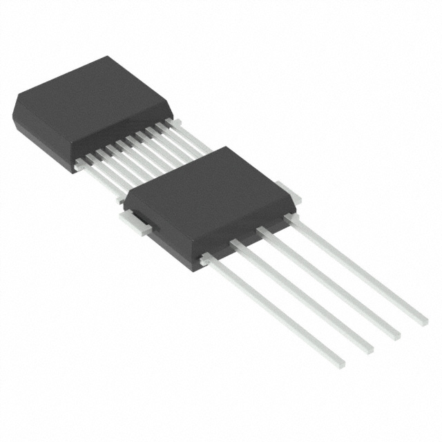


 工商网监
湘ICP备2023018690号
工商网监
湘ICP备2023018690号
