MLX92221LUA-BAA-105-BU 数据手册
MLX92221-AAA
2-Wire Hall Effect Latch
Features and Benefits
▪
▪
▪
▪
▪
▪
▪
▪
Applications
Wide operating voltage range: from 2.7V to 24V
Integrated self-diagnostics
Chopper-stabilized amplifier stage
Programmable Built-in negative temperature
coefficient
Reverse Supply Voltage Protection
Under-Voltage Lockout Protection
Thermal Protection
High ESD rating / Excellent EMC performance
▪
▪
▪
▪
▪
▪
▪
Automotive, Consumer and Industrial
Wiper motor
Window lifter
Seatbelt buckle
Seat positioning
Sunroof/Tailgate opener
Electrical power steering
Ordering information
Part No.
MLX92221LUA-AAA-xxx-BU
MLX92221LSE-AAA-xxx-RE
Temperature Code
L (-40°C to 150°C)
L (-40°C to 150°C)
VDD
UnderVoltage
Lockout
TEST
Temperature
Compensation
Switched
Hall
Plate
Bop/Brp
reference
Thermal
Protection
Output
Current Sink
CDS
Amplifier
Control
Trimming
Register
GND
2. General Description
The Melexis MLX92221 is a new generation of Hall-effect
switches designed in mixed signal submicron CMOS
technology.
The device integrates a voltage regulator, Hall sensor with
advanced offset cancellation system and a current sinkconfigured output driver, all in a single package.
Based on a brand-new platform, the magnetic core is using
an improved offset cancellation system allowing faster and
more accurate processing while being temperature
insensitive and stress independent. In addition, a
temperature coefficient is implemented to compensate the
natural behaviour of certain types of magnets becoming
weaker with rise in temperature.
REVISION 005 – JUNE 29, 2022
390109222102
Comment
BU (Bulk)
RE (Reel)
The included voltage regulator operates from 2.7 to 24V,
hence covering a wide range of applications. With the builtin reverse voltage protection, a serial resistor or diode on
the supply line is not required so that even remote sensors
can be specified for low voltage operation down to 2.7V
while being reverse voltage tolerant.
1. Functional Diagram
Voltage Regulator
with Reverse Polarity
Protection
Package Code
UA (TO92-3L)
SE (TSOT-23)
In an event of a drop below the minimum supply voltage
during operation, the under-voltage lock-out protection will
automatically freeze the device, preventing the electrical
perturbation to affect the magnetic measurement circuitry.
The output current state is therefore only updated based on
a proper and accurate magnetic measurement result.
The two-wire interface not only saves one wire, but also
allows implementation of diagnostic functions as reverse
polarity connection and malfunction detection.
The on-chip thermal protection also switches off the output
if the junction temperature increases above an abnormally
high threshold. It will automatically recover once the
temperature decreases below a safe value.
With latching magnetic characteristics, the supply current
state is turned high by a sufficiently strong South Pole
facing the package branded side. Toggling the state of the
supply current from high to low is possible by applying low
or no magnetic field.
The MLX92221 is delivered in a Green and RoHS compliant
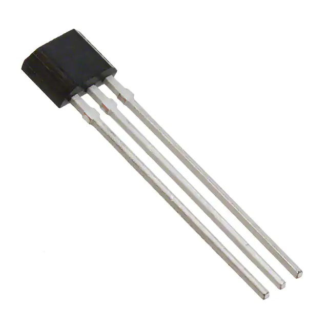
Plastic Single-in-Line (TO-92 flat) for through-hole mount or
PCB-less design or in 3-pin Thin Small Outline Transistor
(TSOT) for surface mount process
Page 1 of 17
�MLX92221-AAA
2-Wire Hall Effect Latch
Contents
Features and Benefits ................................................................................................................................ 1
Applications ............................................................................................................................................... 1
Ordering information ................................................................................................................................. 1
1. Functional Diagram ................................................................................................................................ 1
2. General Description ............................................................................................................................... 1
3. Absolute Maximum Ratings.................................................................................................................... 4
4. General Electrical Specifications............................................................................................................. 5
5. Specifications ......................................................................................................................................... 6
MLX92221LSE-AAA-001 ..................................................................................................................... 6
MLX92221LSE-AAA-002 ..................................................................................................................... 6
MLX92221LSE-AAA-003 ..................................................................................................................... 6
MLX92221LUA-AAA-004 .................................................................................................................... 7
MLX92221LUA-AAA-005 .................................................................................................................... 7
MLX92221LUA-AAA-006 .................................................................................................................... 7
MLX92221LUA-AAA-007 .................................................................................................................... 7
6. Magnetic Behavior ................................................................................................................................. 8
7. Performance Graphs .............................................................................................................................. 9
IOFFLow vs. TJ.......................................................................................................................................... 9
IOFFHigh vs. TJ ........................................................................................................................................ 9
ION vs. TJ ............................................................................................................................................... 9
IOFFLow vs. VDD ....................................................................................................................................... 9
IOFFHigh vs. VDD ...................................................................................................................................... 9
ION vs. VDD ............................................................................................................................................ 9
VDD de-rating ..................................................................................................................................... 10
Power de-rating ................................................................................................................................ 10
8. Application Information ....................................................................................................................... 11
Typical Automotive Application Circuit ........................................................................................... 11
Automotive and Harsh, Noisy Environments Application Circuit .................................................. 11
Strobing VDD application (used for reduced self-heating) .............................................................. 11
9. Standard information regarding the manufacturability of Melexis products ........................................ 12
10. ESD Precautions ................................................................................................................................. 12
11. Package Information .......................................................................................................................... 13
REVISION 005 – JUNE 29, 2022
390109222102
Page 2 of 17
�MLX92221-AAA
2-Wire Hall Effect Latch
TSOT-3L (SE Package) ..................................................................................................................... 13
TO92-3L (UA Package).................................................................................................................... 15
12. Contact .............................................................................................................................................. 17
13. Disclaimer .......................................................................................................................................... 17
REVISION 005 – JUNE 29, 2022
390109222102
Page 3 of 17
�MLX92221-AAA
2-Wire Hall Effect Latch
3. Absolute Maximum Ratings
Parameter
Supply Voltage (1, 2)
Symbol
Value
Units
VDD
+27
V
(1, 2, 3)
IDD
+20
mA
Supply Current (1, 3, 4)
IDD
+50
mA
Reverse Supply Voltage (1, 2)
VDDREV
-24
V
Reverse Supply Current (1, 2, 5)
IDDREV
-20
mA
Reverse Supply Current (1, 4, 5)
IDDREV
-50
mA
Maximum Junction Temperature (6)
TJ
+165
C
Operating Temperature Range
TA
-40 to 150
C
Storage Temperature Range
TS
-55 +165
C
-
3000
V
-
400
V
-
1000
V
B
Unlimited
mT
Supply Current
ESD Sensitivity – HBM
(7)
ESD Sensitivity – MM (8)
ESD Sensitivity – CDM
(9)
Magnetic Flux Density
Exceeding the absolute maximum ratings may cause permanent damage. Exposure to absolute-maximum-rated conditions
for extended periods may affect device reliability.
1
The maximum junction temperature should not be exceeded
For maximum 1 hour
3
Including current through protection device
4
For maximum 1 second
5
Through protection device
6
For 1000 hours
7
Human Model according AEC-Q100-002 standard
8
Machine Model according AEC-Q100-003 standard
9
Charged Device Model according AEC-Q100-011 standard
2
REVISION 005 – JUNE 29, 2022
390109222102
Page 4 of 17
�MLX92221-AAA
2-Wire Hall Effect Latch
4. General Electrical Specifications
DC Operating Parameters VDD = 2.7 to 24V, TJ = -40°C to 165°C (unless otherwise specified)
Min
2.7
Typ (1)
-
Max
24
1
Units
V
mA
2
3.3
5
mA
5
12
0.1
260
6
14.5
0.3
40
340
6.9
17
0.8
1
70
-
mA
mA
mA
μs
μs
kHz
-
7.5
-
µs
-
±3.3
-
µs
30
50
-
kHz
VUVL
-
2
2.7
V
tUVL
-
1
-
µs
-
190 (9)
180 (9)
-
0.8
°C
°C
mA
Parameter
Supply Voltage
Reverse Supply Current
Symbol Test Conditions
VDD
Operating
IDDREV
VDD = -16V
OFF Supply Current
IOFFLow
VDD = 3.5 to 24V
OFF Supply Current
ON Supply Current
Safe Mode Supply Current
Supply Current Rise/Fall Time (2)
Power-On Time (3,4,5)
Chopping Frequency
IOFFHigh
ION
ITP
tRISE/FALL
tON
fCHOP
VDD = 3.5 to 24V
VDD = 3.5 to 24V
Thermal Protection activated
VDD = 12V, CLOAD = 50pF to GND
VDD = 5V, dVDD/dt > 2V/us
Delay time (2,6)
tD
Output Jitter (p-p) (2,7)
tJITTER
Maximum Switching Frequency
(2,8)
Under-voltage Lockout
Threshold
Under-voltage Lockout Reaction
time (2)
Thermal Protection Threshold
Thermal Protection Release
Safe Mode Supply Current
fSW
TPROT
TREL
ITP
UA Package Thermal Resistance
RTH
TSOT Package Thermal
Resistance
RTH
Average value for 1000 successive
switching events @10kHz, Square
wave with B ≥ 3*BOPMAX, tRISE = tFALL
≤20us
Square wave with B ≥ 3*BOPMAX over
1000 successive switching events
@1kHz
B ≥ 3*BOPMAX and square wave
magnetic field
Junction temperature
Junction temperature
Thermal Protection activated
Single layer (1S) Jedec board, zero
LFPM
Single layer (1S) Jedec board, zero
LFPM
200
°C/W
300
°C/W
1
Typical values are defined at T A = +25°C and V DD = 12V
Guaranteed by design and verified by characterization, not production tested
3
The Power-On Time represents the time from reaching V DD = VPOR to the first refresh of the supply current state.
4
Power-On Slew Rate is not critical for the proper device start-up.
5
B>BOPmax + 1 mT for direct output sensors, or B 32V are expected, usage a zener diode DZ1 is recommended. The RSENSE-DZ1
network should be sized to limit the voltage over the device below the maximum
allowed.
MLX 92221 / 41
VDD
V DD
South Pole
12 V
ON phase
( 1 ms)
I DD
weak South or B
OFF phase
( 1s )
= null
t
I ONtyp
Valid I DD
state
Valid I DD
state
IOFFtyp
tON
tON
t
Notes :
1. Given strobe timing is exemplary only .
2. For proper operation , a 10nF to 100nF bypass capacitor should be placed as
close as possible to the V DD and ground pin .
REVISION 005 – JUNE 29, 2022
390109222102
Page 11 of 17
�MLX92221-AAA
2-Wire Hall Effect Latch
9. Standard information regarding the manufacturability of Melexis products
Our products are classified and qualified regarding soldering technology, solderability and moisture sensitivity
level according to following test methods:
Reflow Soldering SMD’s (Surface Mount Devices)
•
•
IPC/JEDEC J-STD-020
Moisture/Reflow Sensitivity Classification for Nonhermetic Solid State Surface Mount Devices
(classification reflow profiles according to table 5-2)
EIA/JEDEC JESD22-A113
Preconditioning of Nonhermetic Surface Mount Devices Prior to Reliability Testing
(reflow profiles according to table 2)
Wave Soldering SMD’s (Surface Mount Devices) and THD’s (Through Hole Devices)
•
•
EN60749-20
Resistance of plastic- encapsulated SMD’s to combined effect of moisture and soldering heat
EIA/JEDEC JESD22-B106 and EN60749-15
Resistance to soldering temperature for through-hole mounted devices
Iron Soldering THD’s (Through Hole Devices)
•
EN60749-15
Resistance to soldering temperature for through-hole mounted devices
Solderability SMD’s (Surface Mount Devices) and THD’s (Through Hole Devices)
•
EIA/JEDEC JESD22-B102 and EN60749-21
Solderability
For all soldering technologies deviating from above mentioned standard conditions (regarding peak temperature,
temperature gradient, temperature profile etc) additional classification and qualification tests have to be agreed upon with
Melexis.
The application of Wave Soldering for SMD’s is allowed only after consulting Melexis regarding assurance of adhesive
strength between device and board.
http://www.melexis.com/Assets/Soldering-Application-Note-and-Recommendations-5446.aspx
Melexis is contributing to global environmental conservation by promoting lead free solutions. For more information on
qualifications of RoHS compliant products (RoHS = European directive on the Restriction Of the use of certain Hazardous
Substances) please visit the quality page on our website: http://www.melexis.com/quality.aspx
10. ESD Precautions
Electronic semiconductor products are sensitive to Electro Static Discharge (ESD).
Always observe Electro Static Discharge control procedures whenever handling semiconductor products.
REVISION 005 – JUNE 29, 2022
390109222102
Page 12 of 17
�MLX92221-AAA
2-Wire Hall Effect Latch
11. Package Information
TSOT-3L (SE Package)
11.1.1. TSOT-3L – Package dimensions
3
1
2
11.1.2. TSOT-3L – Sensitive spot
1
3
2
1.44 ± 0.20 mm
0.87 ± 0.20 mm
3
1
2
0.28 ± 0.03 mm
1.47 ± 0.20 mm
REVISION 005 – JUNE 29, 2022
390109222102
1.16 ± 0.15 mm
Page 13 of 17
�MLX92221-AAA
2-Wire Hall Effect Latch
11.1.3. TSOT-3L – Package marking / Pin definition
Top
3
WW
WWYY
1
2
1
2
YY
Last 2 digits of calendar year
Assembly week
Bottom
LLLL
LLLL
Last 4 digits of lot number
3
Pin #
Name
Type
Function
1
VDD
Supply
Supply Voltage pin
2
TEST
I/O
For Melexis use only
3
GND
Ground
Ground pin
REVISION 005 – JUNE 29, 2022
390109222102
Page 14 of 17
�MLX92221-AAA
2-Wire Hall Effect Latch
TO92-3L (UA Package)
1
2
3
11.2.1. TO92-3L – Package dimensions
11.2.2. TO92-3L – Sensitive spot
3.1 ± 0.13 mm
0.9 ± 0.20 mm
2.05 ± 0.20 mm
1
2
3
1
2
3
0.44 ± 0.03 mm
1.46 ± 0.13 mm
REVISION 005 – JUNE 29, 2022
390109222102
Page 15 of 17
�MLX92221-AAA
2-Wire Hall Effect Latch
11.2.3. TO92-3L – Package marking / Pin definition
Top
4th up to 6th character of lot number
LLL
LLL
YWW
Y
WW
Assembly calendar week
Last digit of year
1
2
3
Pin #
Name
Type
Function
1
VDD
Supply
Supply Voltage pin
2
GND
Ground
Ground pin
3
TEST
I/O
For Melexis use only
REVISION 005 – JUNE 29, 2022
390109222102
Page 16 of 17
�MLX92221-AAA
2-Wire Hall Effect Latch
12. Contact
For the latest version of this document, go to our website at www.melexis.com.
For additional information, please contact our Direct Sales team and get help for your specific needs:
Europe, Africa
Telephone: +32 13 67 04 95
Email : sales_europe@melexis.com
Americas
Telephone: +1 603 223 2362
Email : sales_usa@melexis.com
Asia
Email : sales_asia@melexis.com
13. Disclaimer
The content of this document is believed to be correct and accurate. However, the content of this document is furnished "as is" for informational use only and no representation, nor
warranty is provided by Melexis about its accuracy, nor about the results of its implementation. Melexis assumes no responsibility or liability for any errors or inaccuracies that may
appear in this document. Customer will follow the practices contained in this document under its sole responsibility. This do cumentation is in fact provided without warranty, term,
or condition of any kind, either implied or expressed, including but not limited to warranties of merchantability, satisfactory quality, non-infringement, and fitness for purpose.
Melexis, its employees and agents and its affiliates' and their employees and agents will not be responsible for any loss, however arising, from the use of, or reliance on this document.
Notwithstanding the foregoing, contractual obligations expressly undertaken in writing by Melexis prevail over this disclaimer.
This document is subject to change without notice, and should not be construed as a commitment by Melexis. Therefore, before placing orders or prior to designing the product into
a system, users or any third party should obtain the latest version of the relevant information.
Users or any third party must determine the suitability of the product described in this document for its application, including the level of reliability required and determine whether
it is fit for a particular purpose.
This document as well as the product here described may be subject to export control regulations. Be aware that export might require a prior authorization from competent
authorities. The product is not designed, authorized or warranted to be suitable in applications requiring extended temperature range and/or unusual environmental requirements.
High reliability applications, such as medical life-support or life-sustaining equipment or avionics application are specifically excluded by Melexis. The product may not be used for
the following applications subject to export control regulations: the development, production, processing, operation, maintenance, storage, recognition or proliferation of:
1. chemical, biological or nuclear weapons, or for the development, production, maintenance or storage of missiles for such weapons;
2. civil firearms, including spare parts or ammunition for such arms;
3. defense related products, or other material for military use or for law enforcement;
4. any applications that, alone or in combination with other goods, substances or organisms could cause serious harm to persons or goods and that can be used as a means of
violence in an armed conflict or any similar violent situation.
No license nor any other right or interest is granted to any of Melexis' or third party's intellectual property rights.
If this document is marked “restricted” or with similar words, or if in any case the content of this document is to be reasonably understood as being confidential, the recipient of this
document shall not communicate, nor disclose to any third party, any part of the document without Melexis’ express written consent. The recipient shall take all necessary measures
to apply and preserve the confidential character of the document. In particular, the recipient shall (i) hold document in confidence with at least the same degree of care by which it
maintains the confidentiality of its own proprietary and confidential information, but no less than reasonable care; (ii) restrict the disclosure of the document solely to its employees
for the purpose for which this document was received, on a strictly need to know basis and providing that such persons to whom the document is disclosed are bound by confidentiality
terms substantially similar to those in this disclaimer; (iii) use the document only in connection with the purpose for which this document was received, and reproduce document only
to the extent necessary for such purposes; (iv) not use the document for commercial purposes or to the detriment of Melexis or its customers. The confidentiality obligations set forth
in this disclaimer will have indefinite duration and in any case they will be effective for no less than 10 years from the receipt of this document.
This disclaimer will be governed by and construed in accordance with Belgian law and any disputes relating to this disclaimer will be subject to the exclusive jurisdiction of the courts
of Brussels, Belgium.
The invalidity or ineffectiveness of any of the provisions of this disclaimer does not affect
The previous versions of this document are repealed.
the validity or effectiveness of the other provisions.
Melexis © - No part of this document may be reproduced without the prior written consent of Melexis. (2022)
IATF 16949 and ISO 14001 Certified
REVISION 005 – JUNE 29, 2022
390109222102
Page 17 of 17
�


 工商网监
湘ICP备2023018690号
工商网监
湘ICP备2023018690号
