MAQ5280
25mA, 120V, Low IQ, High PSRR LDO Automotive
General Description
The MAQ5280 is a high performance low dropout regulator, offering a very low noise output with a very wide input voltage operating range, up to 120V DC input voltage. Ideal for high input voltage applications such as automotive and telecom, the MAQ5280 offers 2% initial accuracy, extremely high power supply rejection ratio (PSRR > 80dB) and low ground current (typically 31µA). The MAQ5280 can also be put into a zero-off-mode current state, drawing a minuscule amount of current when disabled. The MAQ5280 has a very wide input voltage range, with a DC rating from –24V to 120V. This wide input range covers the automotive load dump range and the MAQ5280 is optimized for line transient response, making it ideal for harsh environment applications. The MAQ5280 has an operating junction temperature range of –40°C to +125°C and is available in an adjustable output voltage version in a lead-free (RoHS compliant) 8pin EPAD SOIC packaging. This part is also AEC-Q100 Qualified for automotive applications. Data sheets and support documentation can be found on Micrel’s web site at: www.micrel.com.
Features
• • • • • • • • • Wide Input Voltage Range: 4.5V to 120V DC Very Low Quiescent Current: 31µA typical 25mA guaranteed output current Adjustable Output from 1.215V to 5V DC voltage protection down to -24V Ability to withstand up to +120V DC at the input Stable with ceramic output capacitors Ultra High PSRR > 80dB for RF Applications High output accuracy – ± 2% initial accuracy – ± 3% over temperature (–40°C to +125°C) • Thermal shutdown and current limit protection • Thermally efficient 8-pin EPAD SOIC package • AEC-Q100 qualified
Applications
• Automotive Systems • Industrial Applications • Remote Keyless Entry Power Supply • Telecom Applications • Off-line Power Supplies ___________________________________________________________________________________________________________
Typical Application
Automotive Application
Micrel Inc. • 2180 Fortune Drive • San Jose, CA 95131 • USA • tel +1 (408) 944-0800 • fax + 1 (408) 474-1000 • http://www.micrel.com
October 2008
M9999-102708-B
�Micrel, Inc.
MAQ5280
Ordering Information
Part Number MAQ5280YME Voltage Adj. Temperature Range –40° to +125°C Package 8-Pin EPAD SOIC Lead Finish Pb-Free
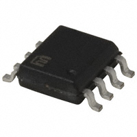
Pin Configuration
CBYP VOUT ADJ GND 1 2 3 4 8 VIN 7 NC 6 NC 5 EN
8-Pin EPAD SOIC (ME)
Pin Description
Pin Number 1 2 3 4 5 6, 7 8 EP Pin Name CBYP VOUT ADJ GND EN NC VIN – Pin Function Connect 10µF capacitor. Increases PSRR when VIN ≥ 6.5V. Regulator Output Pin. Connect 2.2µF for better stable operation. Connect pin 3 to external resistor divider to set VOUT. Ground. Enable pin. Enable Low turns part OFF, Enable High turns part ON. Not internally connected. Supply Input pin. Supply (Input): -24V to 120V input voltage. Exposed Pad – Connect to Ground plane trace.
October 2008
2
M9999-102708-B
�Micrel, Inc.
MAQ5280
Absolute Maximum Ratings(1)
Supply Voltage (VIN) ..................................... –24V to +120V Enable Voltage (VEN)...................................... –1V to +120V Power Dissipation (PD) ........................... Internally Limited(3) Max Reflow Temperature (per IPC/JEDEC 20°C) ..... 260°C Storage Temperature (TS).........................–65°C to +150°C ESD Rating(4) .................................................................. 2kV
Operating Ratings(2)
Supply Voltage (VIN)...................................... 4.5V to +120V Enable Voltage (VEN)........................................ 0V to +120V Junction Temperature (TJ) ........................ –40°C to +125°C Junction Thermal Resistance EPAD SOIC-8 (θJA)............................................41°C/W
Electrical Characteristics(5)
VIN = 12V; VEN = 2V; COUT = 2.2µF; CBYP = 10µF; IOUT = 100µA; TJ = 25°C, bold values indicate –40°C to +125°C, unless noted.
Parameter Output Voltage Accuracy ADJ Pin Voltage Line Regulation
(6) (7)
Condition Variation from nominal VOUT Variation from nominal VOUT, –40°C to +125°C ΔVIN = 6.5V to 120V IOUT = 100µA to 25mA IOUT = 100µA; VIN = 4.5V; Adjust Pin = 0V IOUT = 10mA; VIN = 4.5V; Adjust Pin = 0V IOUT = 25mA; VIN = 4.5V; Adjust Pin = 0V
Min –2 –3
Typ
Max +2 +3
Units % % V % % mV mV mV µA µA µA µA dB mA
1.219 –0.5 –0.5 0 0 0 0 0 0 0 80 40 0.4 70 70 0.03 3 3.3 120 Logic Low Logic High 2.0 0 0 0 0.1 0.02 0.12 0.15 1 1 1 10 VEN ≤ 0.3V; VIN = 12V VEN ≥ 2.0V; VIN = 12V VIN = 4.5V; VEN = 120V 0.3 100 50 10 0.04 0.2 430 800 1100 31 260 0.02 0.5 0.5 700 1000 1500 50 400 1 5
Load Regulation Dropout Voltage
Ground Pin Current Ground Pin Current in Shutdown Ripple Rejection Current Limit IDD Reverse Battery IOUT Reverse Current ADJ Pin Current Output Voltage Noise Enable Input Enable Input Voltage Enable Input Current
IOUT = 100µA IOUT = 25mA VEN ≤ 0.3V VEN ≤ 0.3V, –40°C to +125°C f = up to 1kHz VOUT = 0V; VIN = 4.5V VOUT = 0V; VIN = 14.4V VIN = –24V; VEN = 0.3V VIN = 0V; VOUT = 5V; VEN = 0.3V
mA µA µA nA µVRMS V V µA µA µA ms
Turn-on Time
COUT = 2.2µF; IOUT = 25mA
October 2008
3
M9999-102708-B
�Micrel, Inc.
Notes: 1. Exceeding the absolute maximum rating may damage the device. 2. The device is not guaranteed to function outside its operating rating.
MAQ5280
3. The maximum allowable power dissipation of any TA (ambient temperature) is PD(max) = (TJ(max) – TA) / θJA. Exceeding the maximum allowable power dissipation will result in excessive die temperature, and the regulator will go into thermal shutdown. 4. Devices are ESD sensitive. Handling precautions recommended. Human body model, 1.5kΩ in series with 100pF. 5. Specification for packaged product only. 6. Line regulation is a percentage of VOUT. 7. Regulation is measured at constant junction temperature using low duty cycle pulse testing; changes in output voltage due to heating effects are covered by the thermal regulation specification.
October 2008
4
M9999-102708-B
�Micrel, Inc.
MAQ5280
Typical Characteristics
120 100 80 60 40 20 0 10 100 1000 10000 100000 FREQUENCY (Hz) 10mA 25mA 1mA
Power Supply Rejection Ratio
100µA
3.155 3.154 3.153 3.152 3.151 3.150 3.149 3.148 3.147 3.146 3.145 0
Output Voltage vs. Input Voltage
5.010 5.008 5.006 5.004 5.002 5.000 4.998 4.996 4.994 4.992 4.990 0
Output Voltage vs. Load Current
EN = VBYP VIN = 12V VOUT = 5V CIN = 0.18µF COUT = 2.2µF
VOUT = 3.15V CIN = 0.18µF COUT = 2.2µF Load = 100µA
20
40 60 80 100 120 INPUT VOLTAGE (V)
5 10 15 20 LOAD CURRENT (mA)
25
1.225 1.224 1.223 1.222 1.221 1.220 1.219 1.218 1.217 1.216
Feedback Voltage vs. Temperature
300 250
Ground Current vs. Output Current
35 32 29 26 23
Ground Current vs. Temperature
VIN=120V
–40°C Load=100µA
200 150
120°C 25°C VIN = 12V VOUT = 5V CIN = 0.18µF COUT = 2.2µF
VIN=12V
Load=25mA
VIN=4.5V
100 50 0 0
1.215 -40 -20 0 20 40 60 80 100 120 TEMPERATURE (°C)
5 10 15 20 25 OUTPUT CURRENT (mA)
20 -40 -20 0 20 40 60 80 100 120 TEMPERATURE (°C)
EN = VIN Load = 100µA
1.4 1.2 1.0 0.8 0.6 0.4 0.2 0 0
Dropout Voltage vs. Output Current
VIN = 4.5V CIN = 0.18µF COUT = 2.2µF
5 10 15 20 25 OUTPUT CURRENT (mA)
1.2 1.1 Load=25mA 1.0 0.9 0.8 Load=10mA 0.7 0.6 0.5 0.4 0.3 Load=100µA 0.2 0.1 0 -40 -20 0 20 40 60 80 100 120 TEMPERATURE (°C)
Dropout Voltage vs. Temperature
79 76 73 70 67 64 61 58 55 0
Current Limit vs. Input Voltage
VOUT = 3.15V COUT = 2.2µF
20
40 60 80 100 120 INPUT VOLTAGE (V)
80 77 74 71 68 65 62 59 56 53
Current Limit vs. Temperature
3.40 3.37 3.34 3.31 3.28 3.25 3.22
Adjust Pin Current vs. Temperature
1.1 1.0 0.9 0.8 0.7 0.6 0.5
Enable Threshold vs. Temperature
Load = 100µA
VIN=12V
VIN =4.5V
3.19 3.16 3.13
50 -40 -20 0 20 40 60 80 100 120 TEMPERATURE (°C)
3.10 -40 -20 0 20 40 60 80 100 120 TEMPERATURE (°C)
VEN = 12V
0.4 -40 -20 0 20 40 60 80 100 120 TEMPERATURE (°C)
October 2008
5
M9999-102708-B
�Micrel, Inc.
MAQ5280
Typical Characteristics (continued)
0.20 0.18 0.16 0.14 0.12 0.10 0.08 0.06 0.04 0.02 0 0
Enable Current vs. Enable Voltage
0.135 0.133 0.131 0.129 0.127 0.125 0.123 0.121 0.119 0.117
Enable Current vs. Temperature
Low Voltage Behavior
6.5 5.5
VIN=12V
4.5 3.5
Load=100µA
VIN=120V
2.5 1.5 0.5 0 1.5
Load=10mA
VIN = 12V
20 40 60 80 100 120 ENABLE VOLTAGE (V)
0.115 -40 -20 0 20 40 60 80 100 120 TEMPERATURE (°C)
VOUT = 5V COUT = 2.2µF
2.5 3.5 4.5 5.5 INPUT VOLTAGE (V)
6.5
70 60 50 40 30 20 10 0
VIN C urrent vs. Input Voltage
10
Output Noise Spectral Density
Noise(10Hz to 100kHz)=113µV RMS VIN = 3.6V
1
VOUT = 3.3V COUT = 2.2µF CBYP = 0.1µF Load = 25mA
0.1
VOUT = 1.2V CIN = 0.18µF COUT = 2.2µF I OUT = 0A
0
24 48 72 96 INPUT VOLTAGE (V)
120
0.01 10
100 1k 10k 100k FREQUENCY (Hz)
1M
October 2008
6
M9999-102708-B
�Micrel, Inc.
MAQ5280
Functional Characteristics
October 2008
7
M9999-102708-B
�Micrel, Inc.
MAQ5280
Functional Diagram
VIN
EN >
Bypass Regulator + < EN 1.2V Post Regulator CBYP EN > 1.22V
EN
Enable
EN
EN > EN > GND
VOUT
ADJ
October 2008
8
M9999-102708-B
�Micrel, Inc.
MAQ5280 EN Pin EN pin is a logic level enable input which turns MAQ5280 on/off. Drive EN pin level high to turn the device ON and drive EN pin low to keep the device in shutdown mode. In shutdown mode the MAQ5280 draws typically 20nA from the input supply. EN pin can withstand 120V, allowing EN always connected to input supply for always-ON operation. ADJ Pin ADJ pin gives the flexibility to set the output voltage to the requirement from 1.22V to 5V. Use a resistor divider from output and connect to ADJ pin, internal reference is typically 1.219V. GND Pin This GND pin provides the ground for all the electrical connections. MAQ5280 has exposed pad underneath the package which should be connected to ground. If this exposed pad is connected to wide ground plane it would improve the thermal performance of MAQ5280. NC Pins There are two NC pins on the package which are not connected internally. VOUT Pin The VOUT pin is the regulated output of the post regulator. When the MAQ5280 is enabled, VOUT regulates at a fixed voltage, when disabled, VOUT is high impedance. A 2.2µF or larger ceramic capacitor must be connected to VOUT pin-to-ground.
Functional Description
MAQ5280 is a high performance linear regulator which accepts wide input operating range 4.5V to 120V. This allows the use in harsh environments. The input can surge from 0V to 120V within a millisecond. The first stage bypass regulator isolates output from this input by producing an intermediate head voltage which is a inputto-post regulator. This post regulator gives the control to regulate the required output voltage. The output voltage is adjustable from 1.22V to 5V. VIN Pin VIN pin is the supply input pin. A 0.18µF or larger capacitor with proper voltage rating is recommended for filtering the input voltage variations and noise on the input voltage. This capacitor should be close to the VIN and GND pins. CBYP Pin The Bypass pin is the output of the Bypass regulator and the input of the post regulator. By connecting a capacitor from the CBYP pin-to-GND, a greater stability and a much higher PSRR is achieved. A 10µF ceramic capacitor is recommended and this significantly decreases VOUT noise and perturbations due to line transients. When the MAQ5280 is enabled, the Bypass pin voltage is regulated at 5.5V. To maintain 5.5V regulation and high PSRR, the VIN must be no lower than 6.5V. For VIN less than 6.5V while in dropout, the PSRR is reduced.
October 2008
9
M9999-102708-B
�Micrel, Inc.
MAQ5280 PSRR Power Supply Rejection Ratio is the measure of a VOUT signal caused by a signal on the VIN pin. The ratio of VIN/VOUT in dB is PSRR. The MAQ5280’s PSRR from 0Hz to 1kHz exceeds 80dB. Output Voltage Setting For adjustable regulator, VOUT is programmable from 1.22V to 5.0V. A 2.2µF or larger capacitor must be connected to VOUT pin-to-ground to maintain stability. This capacitor value can be increased without bound. The VOUT capacitor can have an ESR of 0Ω. When VIN is lower than VOUT, VOUT is not pulled low by VIN. A small current, typically 4µA, will sink into VOUT pin. The output voltage is controlled by the feedback resistors (R1 and R2) and can be calculated as follows:
Application Information
MAQ5280 is a linear regulator with a wide operating range of input voltage 4.5V to 120V. The input can go down to –24V without any damage to the device. This feature gives the advantage to use in harsh environment applications such as automotive load dump and remote keyless entry as well as telecom applications. Thermal Protection MAQ5280 has internal thermal shutdown to protect from over dissipation and failure. When the junction temperature exceeds +160°C, an internal thermal sensor signals the shutdown logic to turn off the pass transistor and allows the IC to cool. The thermal sensor turns the pass transistor on again after the junction temperature cools by 10°C. This results in a cycled output during continuous thermal overload conditions. The recovery from thermal shutdown is smooth without any overshoot. For continuous operation, do not exceed the maximum junction temperature rating of +125°C. Current Limit MAQ5280 has a current limit protection to protect it from over loads. The recovery from current limit protection is smooth without any overshoots. The output can be shorted to GND for an indefinite period of time without damage to the device. During a short circuit, the power dissipated across the pass transistor can quickly heat the device. When the die temperature reaches +160°C, the MAQ5280 shut down and automatically restart after the die temperature cools by 10°C. This results in a pulsed output operation. CBYP Output when Enable is Low When the Enable is low and the MAQ5280 is disabled, while VIN voltage is present, the CBYP pin voltage is typically 4.5V, even for VIN as high as 120V. The Bypass regulator although maintaining the Bypass voltage, requires no current from VIN other than leakage current. Bypass Capacitor A 10µF capacitor should be connected from bypass pin to ground to maintain stability of the bypass regulator. The voltage rating of the capacitor must be 8V or higher. Low ESR ceramic capacitors work well. Although a 1µF capacitor maintains good AC power supply rejection, higher capacitance values will enhance AC power supply rejection.
⎛ R1 ⎞ + 1⎟ VOUT = VREF ⋅ ⎜ ⎝ R2 ⎠
VREF = 1.219V The evaluation board is initially adjusted to 5V, but can easily be modified by removing R1 and replacing it with the value that yields the desired output voltage.
⎛V ⎞ R1 = R 2 ⋅ ⎜ OUT − 1⎟ ⎜V ⎟ ⎝ REF ⎠
Ensure the output voltage selected does not exceed 5V.
Enable Pin The voltage on enable pin EN of MAQ5280 could vary from –1V to 120V. So enable pin EN of MAQ5280 can be used in a different configuration as the application dictates. If the MAQ5280 needs to be always enabled then simply connect the EN pin to CBYP pin, as shown in Figure 1. Then whenever VIN has a supply voltage output is developed. Input can swing from –24V to 120V. One can also connect EN pin through 100kΩ resistor to input as shown in Figure 2 to achieve the same result.
October 2008
10
M9999-102708-B
�Micrel, Inc.
MAQ5280
Figure 1. MAQ5280 EN Always Enabled
Figure 2. Enable Connected to VIN Application
October 2008
11
M9999-102708-B
�Micrel, Inc.
MAQ5280
Bill of Materials
Item C1 Part Number NMC-P1210X7R184K200TRPLPF C1812C184K2RAC VJ1812Y184KXC C1608X5R1A225K C2 0603C225MAT GRM188R60J225KE19D C1608X5R0J105K C3 R1 R2 U1
Notes: 1. NIC: www.nic.com 2. Kemet Electronics: www.ketem.com 3. Vishay: www.vishay.com 4. TDK: www.tdk.com 5. AVX: www.avx.com 6. Murata: www.murata.com 7. Micrel, Inc.: www.micrel.com
Manufacturer NIC
(1)
Description Capacitor, 0.18µF, 200V, Size 1210 Capacitor, 0.18µF, 200V, Size 1812 Capacitor, 2.2µF,10V, X5R, Size 0603 Capacitor, 2.2µF,6.3V, X7R, Size 0603 Capacitor, 2.2µF,6.3V, X5R, Size 0603 Capacitor, 1µF,6.3V, X5R, Size 0603 Resistor, 15.4k, 1%, 1/16W, Size 0603 Resistor, 4.8k, 1%, 1/16W, Size 0603
Qty. 1
Kemet(2) Vishay
(3)
TDK(4) AVX(5) Murata TDK
(6) (4)
1
VJ0603G105KXYPW1BC GRM188R60J105KA01D CRCW060315R4FKEYE3 CRCW06034R87FKEYE3 MAQ5280YME
Vishay(3) Murata Vishay
(6)
1 1 1 1
Vishay(3)
(3)
(7)
Micrel, Inc.
25mA, 120V, Low IQ, High PSRR LDO
October 2008
12
M9999-102708-B
�Micrel, Inc.
MAQ5280
PCB Layout Recommendations
Top Layer
Bottom Layer
October 2008
13
M9999-102708-B
�Micrel, Inc.
MAQ5280
Package Information
8-Pin EPAD SOIC (ME)
MICREL, INC. 2180 FORTUNE DRIVE SAN JOSE, CA 95131 USA
TEL +1 (408) 944-0800 FAX +1 (408) 474-1000 WEB http://www.micrel.com
The information furnished by Micrel in this data sheet is believed to be accurate and reliable. However, no responsibility is assumed by Micrel for its use. Micrel reserves the right to change circuitry and specifications at any time without notification to the customer. Micrel Products are not designed or authorized for use as components in life support appliances, devices or systems where malfunction of a product can reasonably be expected to result in personal injury. Life support devices or systems are devices or systems that (a) are intended for surgical implant into the body or (b) support or sustain life, and whose failure to perform can be reasonably expected to result in a significant injury to the user. A Purchaser’s use or sale of Micrel Products for use in life support appliances, devices or systems is a Purchaser’s own risk and Purchaser agrees to fully indemnify Micrel for any damages resulting from such use or sale. © 2008 Micrel, Incorporated.
October 2008
14
M9999-102708-B
�


 工商网监
湘ICP备2023018690号
工商网监
湘ICP备2023018690号
