16Gb, 32Gb: x4, x8 3DS DDR4 SDRAM
Description
3-Dimensional Stack (3DS) DDR4 SDRAM
MT40A4G4, MT40A8G4, MT40A2G8, MT40A4G8
Description
Options
• 2H configurations
– 128 Meg x 4 x 16 banks x 2 ranks
– 64 Meg x 8 x 16 banks x 2 ranks
• 4H configurations
– 128 Meg x 4 x 16 banks x 4ranks
– 64 Meg x 8 x 16 banks x 4 ranks
• FBGA package (Pb-free)
– 2H 78-ball FBGA
(8.0mm x 12mm x 1.2mm) Die Rev :G
– 2H 78-ball FBGA
(7.5mm x 11mm x 1.2mm) Die Rev :E
– 4H 78-ball FBGA
(8.0mm x 12mm x 1.2mm) Die Rev :G
– 4H 78-ball FBGA
(7.5mm x 11mm x 1.2mm) Die Rev :E
• Timing – cycle time1
– 0.625ns @ CL = 26 (DDR4-3200)
– 0.682ns @ CL = 24 (DDR4-2933)
– 0.750ns @ CL = 22 (DDR4-2666)
– 0.833ns @ CL = 19 (DDR4-2400)
– 0.833ns @ CL = 20 (DDR4-2400)
– 0.937ns @ CL = 18 (DDR4-2133)
• Self refresh
– Standard
• Operating temperature
– Commercial (0°C ≤ T C ≤ 95°C)
• Revision
The 16Gb, 2-high (2H) and 32Gb, 4-high (4H) 3-dimensional stack (3DS) DDR4 SDRAM use Micron’s
special 3DS 8Gb DDR4 SDRAM organized as two or
four logical ranks. Refer to Micron’s 8Gb DDR4
SDRAM data sheet for the specifications not included
in this document. Specifications for base part number
MT40A2G4 correspond to 2H 3DS manufacturing part
number MT40A4G4 and to 4H 3DS manufacturing
part number MT40A8G4; specifications for base part
number MT40A1G8 correspond to 2H 3DS manufacturing part number MT40A2G8 and to 4H 3DS manufacturing part number MT40A4G8.
Features
• Uses Micron 3DS 8Gb die
• Single electrical signal load for each command, address and data pin
• Two or four logical ranks (includes one or two 2C
pins)
• Each rank has 4 groups of 4 internal banks for concurrent operation
• VDD = V DDQ = 1.2V (1.14–1.26V)
• 1.2V V DDQ-terminated I/O
• JEDEC-standard ball-out
• Low-profile package
• TC of 0°C to 95°C
– 0°C to 85°C: 8192 refresh cycles in 64ms
– 85°C to 95°C: 8192 refresh cycles in 32ms
CCMTD-1725822587-10122
16gb_32gb_3ds.pdf - Rev. C 02/19 EN
Notes:
1
Marking
4G4
2G8
8G4
4G8
HPR
DVN
KVA
CLU
-062H
-068H
-075H
-083J
-083H
-093H
None
None
:G, :E
1. CL = CAS (READ) latency.
2. Not all options listed can be combined to
define an offered product. Use the part catalog search on http://www.micron.com for
available offerings.
Micron Technology, Inc. reserves the right to change products or specifications without notice.
© 2018 Micron Technology, Inc. All rights reserved.
Products and specifications discussed herein are subject to change by Micron without notice.
�16Gb, 32Gb: x4, x8 3DS DDR4 SDRAM
Description
Table 1: Key Timing Parameters
Speed Grade1
Data Rate
(MT/s)
Target CL-nRCD-nRP
-062H
3200
26-22-22
16.25
13.75
13.75
-068H
2933
24-21-21
16.37
14.32 (14.06)
14.32 (14.06)
-075H
2666
22-19-19
16.50
14.25 (14.06)
14.25 (14.06)
-083J
2400
19-17-17
15.83
14.16 (14.06)
14.16 (13.75)
-083H
2400
20-17-17
16.67
14.16 (14.06)
14.16 (14.06)
16.88
14.06
14.06
tAA
-093H
2133
18-15-15
Note: 1. Refer to the Speed Bin Tables for additional
details.
(ns)
tRCD
tRP
(ns)
(ns)
Table 2: 2H Addressing
Parameter
Configuration
4096 Meg x 4
2048 Meg x 8
128 Meg x 4 x 16 banks x 2 ranks
64 Meg x 8 x 16 banks x 2 ranks
Logical rank address
C[0]
C[0]
Bank group address
BG[1:0]
BG[1:0]
4
4
Bank count per group
Bank address in bank group
BA[1:0]
BA[1:0]
128K A[16:0]
64K A[15:0]
1K A[9:0]
1K A[9:0]
8192 Meg x 4
4096 Meg x 8
128 Meg x 4 x 16 banks x 4 ranks
64 Meg x 8 x 16 banks x 4 ranks
Logical rank address
C[1:0]
C[1:0]
Bank group address
BG[1:0]
BG[1:0]
4
4
BA[1:0]
BA[1:0]
128K A[16:0]
64K A[15:0]
1K A[9:0]
1K A[9:0]
Row address
Column address
Table 3: 4H Addressing
Parameter
Configuration
Bank count per group
Bank address in bank group
Row address
Column address
CCMTD-1725822587-10122
16gb_32gb_3ds.pdf - Rev. C 02/19 EN
2
Micron Technology, Inc. reserves the right to change products or specifications without notice.
© 2018 Micron Technology, Inc. All rights reserved.
�16Gb, 32Gb: x4, x8 3DS DDR4 SDRAM
Description
Contents
Important Notes and Warnings ......................................................................................................................... 6
3DS (Master/Slave) Overview ............................................................................................................................ 7
Functionality .................................................................................................................................................... 8
Addressing ................................................................................................................................................. 10
All-Die Commands vs. Single-Die Commands ............................................................................................. 10
Initialization and Reset ................................................................................................................................... 11
Mode Register Set ........................................................................................................................................... 11
Unique 3DS MRS Values for Mode Register 1 ............................................................................................... 11
Multipurpose Register ................................................................................................................................ 12
Post Package Repair .................................................................................................................................... 12
Command/Address Parity ............................................................................................................................... 12
Calibration ..................................................................................................................................................... 13
ACTIVE Operation .......................................................................................................................................... 14
Column Access Operation (WRITE and READ) Timings .................................................................................... 16
READ Operation ............................................................................................................................................. 18
READ Operation Examples ......................................................................................................................... 18
WRITE Operations .......................................................................................................................................... 21
WRITE Operation Examples ........................................................................................................................ 21
PRECHARGE Commands ................................................................................................................................ 23
REFRESH Operation ....................................................................................................................................... 23
SELF REFRESH Operation ............................................................................................................................... 24
Power-Down Operations ................................................................................................................................. 25
On-Die Termination (ODT) ............................................................................................................................. 25
DRAM Package Electrical Specifications .......................................................................................................... 26
Speed Bin Tables ............................................................................................................................................ 29
Current Specifications – Measurement Conditions ........................................................................................... 46
IDD, IPP, and IDDQ Measurement Conditions ................................................................................................. 46
IDD Definitions ........................................................................................................................................... 48
Current Specifications – Patterns and Test Conditions ...................................................................................... 51
Current Test Definitions and Patterns .......................................................................................................... 51
IDD Specifications ....................................................................................................................................... 64
Current Specifications – Limits ........................................................................................................................ 65
Package Dimensions ....................................................................................................................................... 73
Thermal Characteristics .................................................................................................................................. 74
CCMTD-1725822587-10122
16gb_32gb_3ds.pdf - Rev. C 02/19 EN
3
Micron Technology, Inc. reserves the right to change products or specifications without notice.
© 2018 Micron Technology, Inc. All rights reserved.
�16Gb, 32Gb: x4, x8 3DS DDR4 SDRAM
Description
List of Figures
Figure 1: 2-High 3DS Functional Block Diagram ............................................................................................... 8
Figure 2: 4-High 3DS Functional Block Diagram ............................................................................................... 9
Figure 3: CA Parity Error During Refresh ......................................................................................................... 13
Figure 4: tRRD and tFAW Timing Example ...................................................................................................... 14
Figure 5: READ BL8 to READ BL8 (tCCD = 4) Example ..................................................................................... 19
Figure 6: READ BL8 to READ BL8 (tCCD = 5) Example ..................................................................................... 19
Figure 7: READ BL8 to READ BL8 (tCCD = 6) Example ..................................................................................... 20
Figure 8: WRITE BL8 to WRITE BL8 ( tCCD = 4) Example .................................................................................. 22
Figure 9: WRITE BL8 to WRITE BL8 ( tCCD > 4) Example .................................................................................. 22
Figure 10: REFRESH-to-REFRESH Command Timing Example ....................................................................... 24
Figure 11: SELF REFRESH Command Timing Example ................................................................................... 25
Figure 12: Measurement Setup and Test Load for I DDx, IPPx and IDDQx .............................................................. 47
Figure 13: Correlation: Simulated Channel I/O Power to Actual Channel I/O Power ......................................... 47
Figure 14: 78-Ball FBGA Die Rev. G (package codes HPR and KVA) ................................................................... 73
Figure 15: Thermal Measurement Point ......................................................................................................... 74
CCMTD-1725822587-10122
16gb_32gb_3ds.pdf - Rev. C 02/19 EN
4
Micron Technology, Inc. reserves the right to change products or specifications without notice.
© 2018 Micron Technology, Inc. All rights reserved.
�16Gb, 32Gb: x4, x8 3DS DDR4 SDRAM
Description
List of Tables
Table 1: Key Timing Parameters ....................................................................................................................... 2
Table 2: 2H Addressing .................................................................................................................................... 2
Table 3: 4H Addressing .................................................................................................................................... 2
Table 4: 3DS Signals ...................................................................................................................................... 10
Table 5: 2H Stack Addressing ......................................................................................................................... 10
Table 6: 4H Stack Addressing ......................................................................................................................... 10
Table 7: Commands/Operations vs. Ranks Impacted ...................................................................................... 10
Table 8: Truth Table for MRS Commands ........................................................................................................ 11
Table 9: MR1 Register Definition .................................................................................................................... 12
Table 10: 3DS Device tRRD and tFAW Timing at 1600/1866/2133/2400 ............................................................. 14
Table 11: 3DS Device tRRD and tFAW Timing at 2666/2933/3200 ..................................................................... 15
Table 12: Minimum Column-to-Column Timing for 2-High and 4-High Stacks at 1600/1866/2133/2400/2666 ... 16
Table 13: Minimum Column-to-Column Timing for 2-High and 4-High Stacks at 2933/3200 ............................ 17
Table 14: Refresh Timing Parameters .............................................................................................................. 23
Table 15: Allowable SELF REFRESH Commands ............................................................................................. 24
Table 16: DRAM Provisional Package Electrical Specifications for x4 and x8 3DS Devices .................................. 26
Table 17: Pad Input/Output Provisional Capacitance for x4 and x8 3DS Devices ............................................... 28
Table 18: DDR4-1600 3DS Speed Bins and Operating Conditions ..................................................................... 30
Table 19: DDR4-1866 3DS Speed Bins and Operating Conditions ..................................................................... 32
Table 20: DDR4-2133 3DS Speed Bins and Operating Conditions ..................................................................... 34
Table 21: DDR4-2400 3DS Speed Bins and Operating Conditions ..................................................................... 36
Table 22: DDR4-2666 3DS Speed Bins and Operating Conditions ..................................................................... 38
Table 23: DDR4-2933 3DS Speed Bins and Operating Conditions ..................................................................... 40
Table 24: DDR4-3200 3DS Speed Bins and Operating Conditions ..................................................................... 43
Table 25: Basic IDD, IPP and IDDQ Measurement Conditions ............................................................................. 48
Table 26: IDD0 and IPP0 Measurement-Loop Pattern1 ....................................................................................... 51
Table 27: IDD1 Measurement-Loop Pattern1 .................................................................................................... 52
Table 28: IDD2N, IDD3N and IPP3P Measurement-Loop Pattern1 .......................................................................... 54
Table 29: IDD2NT Measurement-Loop Pattern1 ................................................................................................ 55
Table 30: IDD4R Measurement-Loop Pattern1 .................................................................................................. 56
Table 31: IDD4W Measurement-Loop Pattern1 .................................................................................................. 57
Table 32: IDD4Wc Measurement-Loop Pattern1 ................................................................................................ 58
Table 33: IDD5B1 Measurement-Loop Pattern1 ................................................................................................. 59
Table 34: IDD5B2 Measurement-Loop Pattern1 ................................................................................................. 61
Table 35: IDD7 Measurement-Loop Pattern1 .................................................................................................... 63
Table 36: Timings used for I DD, IPP, and IDDQ Measurement – Loop Patterns .................................................... 64
Table 37: 2-High IDD, IPP and IDDQ Current Limits; Die Rev. G (0° ≤ T C ≤ 85°C) ................................................... 65
Table 38: 4-High IDD, IPP and IDDQ Current Limits; Die Rev. G (0° ≤ T C ≤ 85°C) ................................................... 66
Table 39: 2-High IDD, IPP and IDDQ Current Limits; Die Rev. E (0° ≤ T C ≤ 85°C) ................................................... 68
Table 40: 4-High IDD, IPP and IDDQ Current Limits; Die Rev. E (0° ≤ T C ≤ 85°C) ................................................... 70
Table 41: Thermal Characteristics .................................................................................................................. 74
CCMTD-1725822587-10122
16gb_32gb_3ds.pdf - Rev. C 02/19 EN
5
Micron Technology, Inc. reserves the right to change products or specifications without notice.
© 2018 Micron Technology, Inc. All rights reserved.
�16Gb, 32Gb: x4, x8 3DS DDR4 SDRAM
Important Notes and Warnings
Important Notes and Warnings
Micron Technology, Inc. ("Micron") reserves the right to make changes to information published in this document,
including without limitation specifications and product descriptions. This document supersedes and replaces all
information supplied prior to the publication hereof. You may not rely on any information set forth in this document if you obtain the product described herein from any unauthorized distributor or other source not authorized
by Micron.
Automotive Applications. Products are not designed or intended for use in automotive applications unless specifically designated by Micron as automotive-grade by their respective data sheets. Distributor and customer/distributor shall assume the sole risk and liability for and shall indemnify and hold Micron harmless against all claims,
costs, damages, and expenses and reasonable attorneys' fees arising out of, directly or indirectly, any claim of
product liability, personal injury, death, or property damage resulting directly or indirectly from any use of nonautomotive-grade products in automotive applications. Customer/distributor shall ensure that the terms and conditions of sale between customer/distributor and any customer of distributor/customer (1) state that Micron
products are not designed or intended for use in automotive applications unless specifically designated by Micron
as automotive-grade by their respective data sheets and (2) require such customer of distributor/customer to indemnify and hold Micron harmless against all claims, costs, damages, and expenses and reasonable attorneys'
fees arising out of, directly or indirectly, any claim of product liability, personal injury, death, or property damage
resulting from any use of non-automotive-grade products in automotive applications.
Critical Applications. Products are not authorized for use in applications in which failure of the Micron component could result, directly or indirectly in death, personal injury, or severe property or environmental damage
("Critical Applications"). Customer must protect against death, personal injury, and severe property and environmental damage by incorporating safety design measures into customer's applications to ensure that failure of the
Micron component will not result in such harms. Should customer or distributor purchase, use, or sell any Micron
component for any critical application, customer and distributor shall indemnify and hold harmless Micron and
its subsidiaries, subcontractors, and affiliates and the directors, officers, and employees of each against all claims,
costs, damages, and expenses and reasonable attorneys' fees arising out of, directly or indirectly, any claim of
product liability, personal injury, or death arising in any way out of such critical application, whether or not Micron or its subsidiaries, subcontractors, or affiliates were negligent in the design, manufacture, or warning of the
Micron product.
Customer Responsibility. Customers are responsible for the design, manufacture, and operation of their systems,
applications, and products using Micron products. ALL SEMICONDUCTOR PRODUCTS HAVE INHERENT FAILURE RATES AND LIMITED USEFUL LIVES. IT IS THE CUSTOMER'S SOLE RESPONSIBILITY TO DETERMINE
WHETHER THE MICRON PRODUCT IS SUITABLE AND FIT FOR THE CUSTOMER'S SYSTEM, APPLICATION, OR
PRODUCT. Customers must ensure that adequate design, manufacturing, and operating safeguards are included
in customer's applications and products to eliminate the risk that personal injury, death, or severe property or environmental damages will result from failure of any semiconductor component.
Limited Warranty. In no event shall Micron be liable for any indirect, incidental, punitive, special or consequential
damages (including without limitation lost profits, lost savings, business interruption, costs related to the removal
or replacement of any products or rework charges) whether or not such damages are based on tort, warranty,
breach of contract or other legal theory, unless explicitly stated in a written agreement executed by Micron's duly
authorized representative.
CCMTD-1725822587-10122
16gb_32gb_3ds.pdf - Rev. C 02/19 EN
6
Micron Technology, Inc. reserves the right to change products or specifications without notice.
© 2018 Micron Technology, Inc. All rights reserved.
�16Gb, 32Gb: x4, x8 3DS DDR4 SDRAM
3DS (Master/Slave) Overview
3DS (Master/Slave) Overview
The 3DS DDR4 SDRAM provides enhanced functionality and performance when compared to a traditional stacked DDR4 SDRAM device. This data sheet details the product's unique features; providing package dimensions, functional block diagrams, and
electrical and timing specifications as applicable. Topics not addressed in this data
sheet are covered in the standard Micron DDR4 SDRAM data sheet.
The 3DS device provides a stack of DRAM die with one die configured as the master and
the remaining die in the stack configured as slave device(s). Each die functions as a different logical rank. Because the master die provides isolation (or buffering) to the slave
die, the electrical signal loading of the external interface is that of a single DDR4
SDRAM, which can improve timing, bus speeds, and signal integrity while lowering
power consumption—a significant benefit over a traditional stacked device.
CCMTD-1725822587-10122
16gb_32gb_3ds.pdf - Rev. C 02/19 EN
7
Micron Technology, Inc. reserves the right to change products or specifications without notice.
© 2018 Micron Technology, Inc. All rights reserved.
�16Gb, 32Gb: x4, x8 3DS DDR4 SDRAM
Functionality
Functionality
The 3DS DDR4 SDRAM is a high-speed, CMOS dynamic random access memory built
as a 2-high or 4-high 3DS component. The 2-high device consists of one master die and
one slave die. The 4-high device consists of one master die and three slave die. The bottom die will always be the master and any stacked die will be a slave.
Figure 1: 2-High 3DS Functional Block Diagram
Slave Die
Mode Registers
Local
Control
Logic
Core
Memory
Array
Master Die
ZQ
ZQ CAL
ODT Control
ODT
C0
CS#
RAS#
CAS#
WE#
Command
Decode
DLL
Local
Control
Logic
Core
Memory
Array
CCMTD-1725822587-10122
16gb_32gb_3ds.pdf - Rev. C 02/19 EN
Address
Registers
DQ[n-0]
DQS, DQS#
WRITE
Drivers and
input Logic
Mode Registers
A[15: 0]
BG[1:0]
BA[1:0]
READ
Drivers
ODT
VSSQ
Master
Control
Logic
ODT
RZQ
RESET#
CKE
CK, CK#
DM
8
Micron Technology, Inc. reserves the right to change products or specifications without notice.
© 2018 Micron Technology, Inc. All rights reserved.
�16Gb, 32Gb: x4, x8 3DS DDR4 SDRAM
Functionality
Figure 2: 4-High 3DS Functional Block Diagram
Slave Die (C[1:0] = 11)
Mode Registers
Core
Memory
Array
Local
Control
Logic
Slave Die (C[1:0] = 10)
Mode Registers
Local
Control
Logic
Core
Memory
Array
Slave Die (C[1:0] = 01)
Mode Registers
Local
Control
Logic
Core
Memory
Array
ZQ
ZQ CAL
ODT Control
VSSQ
C[1:0]
CS#
RAS#
CAS#
WE#
Command
Decode
Local
Control
Logic
Core
Memory
Array
CCMTD-1725822587-10122
16gb_32gb_3ds.pdf - Rev. C 02/19 EN
READ
Drivers
Address
Registers
DQ[n-0]
DQS, DQS#
WRITE
Drivers and
input Logic
Mode Registers
A[15: 0]
BG[1:0]
BA[1:0]
DLL
ODT
RZQ
Master Die (C[1:0] = 00)
Master
Control
Logic
ODT
ODT
RESET#
CKE
CK, CK#
DM
9
Micron Technology, Inc. reserves the right to change products or specifications without notice.
© 2018 Micron Technology, Inc. All rights reserved.
�16Gb, 32Gb: x4, x8 3DS DDR4 SDRAM
Functionality
Addressing
Each die within the 3DS stack uses the same addressing as its like-density monolithic
device. A 2-high stack has two independent selectable logical ranks; a 4-high stack has
four independent selectable logical ranks. In contrast to conventionally stacked DDR4
(TwinDie), 3DS stacks only have one CS_n pin regardless of the number of die; die (logical rank) selection is accomplished by the state of the Chip ID (Cx) pin(s), which behave
as rank address(es). Because logic is shared between master and slave(s) on the 3DS device, some commands and operations affect all ranks while others only impact a single
rank.
Table 4: 3DS Signals
Configuration
Number of Die (Logical Ranks)
Relevant Signals
16Gb (2-high) 3DS addressing – 8Gb die
2
CS_n, C0
32Gb (4-high) 3DS addressing – 8Gb die
4
CS_n, C0, C1
Table 5: 2H Stack Addressing
Logical Rank Selected
CS_n
C0
0
L
L
1
L
H
Table 6: 4H Stack Addressing
Logical Rank Selected
CS_n
C1
C0
0
L
L
L
1
L
L
H
2
L
H
L
3
L
H
H
All-Die Commands vs. Single-Die Commands
Some commands issued to the 3DS stack device only impact the function of a single
rank (providing the host controller with the best functionality), while others affect all of
the ranks (because of the shared nature of the logic).
Table 7: Commands/Operations vs. Ranks Impacted
Command/Operation
Ranks Impacted
Notes
Mode register
All
One mode register sets condition for all die/ranks
Gear-down mode sync
All
Single electrical interface
Write leveling
All
Single electrical interface
ZQ CAL
All
Single electrical interface
ODT
All
Single electrical interface
Power-down (including SELF REFRESH)
All
Single CKE
CCMTD-1725822587-10122
16gb_32gb_3ds.pdf - Rev. C 02/19 EN
10
Micron Technology, Inc. reserves the right to change products or specifications without notice.
© 2018 Micron Technology, Inc. All rights reserved.
�16Gb, 32Gb: x4, x8 3DS DDR4 SDRAM
Initialization and Reset
Table 7: Commands/Operations vs. Ranks Impacted (Continued)
Command/Operation
Ranks Impacted
Notes
ACTIVE
By rank
New tRRD/tFAW timings
WRITE
By rank
New tCCD timings
READ
By rank
New tCCD timings
PRECHARGE
By rank
Precharge all restrictions
REFRESH
By rank
New tRFC timing to stagger refresh
Initialization and Reset
The 3DS device requires a complete power-up and initialization sequence, which follows the standard DDR4 SDRAM requirement. Mode register commands affect the operation of all die, so there is no need to send mode register commands to each die individually. The 3DS device has special mode register set (MRS) requirements described in
the following section; all other power-up and reset timings and conditions follow the
normal operations listed in the DDR4 SDRAM specification.
Mode Register Set
Standard mode register locations and definitions apply to the 3DS device as described
in the DDR4 SDRAM specification, except as outlined in this section. Any valid MRS
command sets the operating mode for all logical ranks. As such, prior to an MRS command, all logical ranks must be precharged and tRP must be met. In addition, tMRD and
tMOD apply to MRS commands for the 3DS component.
Table 8: Truth Table for MRS Commands
DRAM Command1
CS#
C2
C1
C0
Status
MODE REGISTER SET
L
V
V
V
MRS affects all logical ranks
MODE REGISTER SET
H
V
V
V
All Ranks see DESELECT
Any other command
H
V
V
V
All Ranks see DESELECT
Note:
1. H = High logic level, L = Low logic level, V = H or L (but a defined logic level).
Unique 3DS MRS Values for Mode Register 1
The additional latency settings of the 3DS device requires support for additive latency
of 3 (AL = CL - 3). This setting is required if tAA > tRCD. See Speed Bin tables for more
information.
CCMTD-1725822587-10122
16gb_32gb_3ds.pdf - Rev. C 02/19 EN
11
Micron Technology, Inc. reserves the right to change products or specifications without notice.
© 2018 Micron Technology, Inc. All rights reserved.
�16Gb, 32Gb: x4, x8 3DS DDR4 SDRAM
Command/Address Parity
Table 9: MR1 Register Definition
Mode
Register
4, 3
Description
Additive latency (AL) – Command additive latency setting
00 = 0 (AL disabled)
01 = CL - 11
10 = CL - 2
11 = CL - 3
1. The additive latency settings for the 3DS device are some different than for monolithic
device. The setting AL = CL - 3 may be useful where nCL > nRCD + 2.
Note:
Multipurpose Register
When CA parity or Write CRC are enabled and an error is detected, the 3DS DDR4 device reports the latched states of C[2:0] for the error cycle in multipurpose register(MPR) Page 1 MPR3[2:0]. This is shown in the MPR Page and MPRx Definitions table
in the standard DDR4 data sheet. In the case of 2H and 4H stacks, where not all C[2:0]
pins are used, the unused bits report zero.
Post Package Repair
Post package repair (PPR) is supported on 3DS components and functions largely the
same as on monolithic components. For 3DS devices, the host also provides the die
(logical rank) address on the C[2:0] pins for the ACT command associated with the repair row address, and REFRESH is the only operation allowed by the host on any die
while in PPR mode.
Command/Address Parity
Because command/address (CA) parity provides protection against errors on the command/address bus and the 3DS device has only one electrical interface, parity errors
may impact operations on all die (logical ranks). Otherwise, with the exception of REFRESH operations discussed below, CA parity on the 3DS device functions largely the
same as on the monolithic component.
After a REF command has been issued, a monolithic DDR4 component allows only DESELECT commands until tRFC is satisfied, alleviating the device from having to validate
commands for correct parity during this time. A 3DS device allows commands to be
latched to one rank while another has a refresh in progress; as a result, the 3DS device
has the following behaviors with respect to CA parity:
• A 3DS device continues to calculate CA parity even while refreshes are ongoing
• The CA parity error recovery process shouldn't interrupt refresh(es) that may be in
progress
• The CA parity error recovery process returns to a precharge-all state except for any
rank(s) already refreshing
• MRS commands must wait until tRFC(SLR) is complete for all refreshes in progress
(this is also true for accessing MPR mode)
CCMTD-1725822587-10122
16gb_32gb_3ds.pdf - Rev. C 02/19 EN
12
Micron Technology, Inc. reserves the right to change products or specifications without notice.
© 2018 Micron Technology, Inc. All rights reserved.
�16Gb, 32Gb: x4, x8 3DS DDR4 SDRAM
Calibration
Figure 3: CA Parity Error During Refresh
CK_c
T0
Ta0
Tb0
Tb1
Tb2
Tc0
REF4
Valid 2
Valid 2
Error
Valid
Valid
Td0
Td1
Td2
Te0
Te1
Tf0
Tf1
Valid
DES
DES
DES
Valid1 5
Valid1 5
Valid2 3, 6
CK_t
Command/
Address
tRFC
(SLR)
ALERT_n
tPAR_UNKNOWN
tPAR_ALERT_ON
tPAR_ALERT_PW
tRp_CA_Parity
tRp_CA_Parity
Time Break
Command execution unknown
Command not executed
Command executed
Notes:
1. DRAM is emptying queues. Precharge all and parity checking are off until parity error
status bit is cleared.
2. Command execution is unknown; the corresponding DRAM internal state change may
or may not occur. The DRAM controller should consider both cases and make sure that
the command sequence meets the specifications.
3. Normal operation with parity latency (CA parity persistent error mode disabled). Parity
checking is off until parity error status bit is cleared.
4. When a REF command is issued in tPART_UNKNOWN range, REF may not be executed;
the host should wait tRFC(SLR) to issue valid commands to the same logical rank.
5. Valid commands to the rank with no on-going REF commands are available.
6. Valid commands to the rank with on-going REF commands, including MRS, are available.
Calibration
All configurations of the 3DS device use only a single ZQ pin, which has the same functionality as that of a standard DDR4 SDRAM device. The 3DS device should be considered a single device from the standpoint of calibration. ZQCL commands are required
during the normal initialization and/or reset sequences. ZQCS commands are also required for the 3DS device. When a ZQ command is issued, all ranks must be idle (all
banks precharged with only NOP/DES commands) until the calibration sequence is
complete. All DDR4 SDRAM core ZQ timing parameters and conditions apply simultaneously to all die within the 3DS stack; after a ZQ command has been issued, the appropriate timing must be met before issuing another ZQ command, regardless of the status
of the C[2:0] pins.
CCMTD-1725822587-10122
16gb_32gb_3ds.pdf - Rev. C 02/19 EN
13
Micron Technology, Inc. reserves the right to change products or specifications without notice.
© 2018 Micron Technology, Inc. All rights reserved.
�16Gb, 32Gb: x4, x8 3DS DDR4 SDRAM
ACTIVE Operation
ACTIVE Operation
Restrictions for ACT commands to banks of the same logical rank (SLR) follow the
standard DDR4 SDRAM specification, that is, tRRD and tFAW apply to 3DS devices as
tRRD
t
(SLR) and FAW(SLR). ACT commands to different logical ranks (DLR) must be sepat
rated by RRD(DLR) as shown in the figure and table below. The rate at which groups of
four ACT commands can be issued to different die is given by tFAW(DLR), which is always
16 clocks for every speed, configuration and density.
Figure 4: tRRD and tFAW Timing Example
CK#
CK
Command
ACT
ACT
ACT
tRRD
(SLR)
ACT
ACT
tRRD
(SLR)
Cm
Cn
tRRD
(DLR)
Cm
tRRD
Address
Valid
Valid
Valid
(SLR)
Cn
Cm
Valid
Cm
Valid
Valid
Valid
Valid
Valid
Valid
Valid
Valid
tRRD
(DLR)
(DLR)
tFAW
ACT
tRRD
(SLR)
tFAW
Die Address (Cx)
Valid
(DLR)
Valid
Valid
Time Break
Don’t Care
Table 10: 3DS Device tRRD and tFAW Timing at 1600/1866/2133/2400
Symbol
Description
tRRD
(SLR)
Active-to-Active
(same logical rank)
tRRD
(DLR)
Refresh or Active-to-Active
(different logical ranks)
tFAW
Four active windows
(same logical rank)
(SLR)
DDR4-1600
DDR4-1866
DDR4-2133
DDR4-2400
Units
Short
MAX
(4nCK, 5ns)
MAX
(4nCK, 4.2ns)
MAX
(4nCK, 3.7ns)
MAX
(4nCK, 3.3ns)
CK/ns
Long
MAX
(4nCK, 6ns)
MAX
(4nCK, 5.3ns)
MAX
(4nCK, 5.3ns)
MAX
(4nCK, 4.9ns)
CK/ns
4
4
4
4
CK
x4
MAX (16nCK,
20ns)
MAX (16nCK,
17ns)
MAX (16nCK,
15ns)
MAX (16nCK,
13ns)
CK/ns
x8
MAX
(20nCK, 25ns)
MAX
(20nCK, 23ns)
MAX
(20nCK, 21ns)
MAX
(20nCK, 21ns)
CK/ns
16
16
16
16
CK
MAX (5nCK,
tRFC
(SLR)min
+10ns)
MAX (5nCK,
tRFC
(SLR)min
+10ns)
MAX (5nCK,
tRFC
(SLR)min
+10ns)
MAX (5nCK,
tRFC
(SLR)min
+10ns)
CK/ns
tFAW
Four active windows
(different logical ranks)
tXS
Exit Self-Refresh to commands
not requiring a locked DLL
(DLR)
CCMTD-1725822587-10122
16gb_32gb_3ds.pdf - Rev. C 02/19 EN
14
Micron Technology, Inc. reserves the right to change products or specifications without notice.
© 2018 Micron Technology, Inc. All rights reserved.
�16Gb, 32Gb: x4, x8 3DS DDR4 SDRAM
ACTIVE Operation
Table 11: 3DS Device tRRD and tFAW Timing at 2666/2933/3200
Symbol
Description
tRRD
Active-to-Active
(same logical rank)
(SLR)
tRRD
(DLR)
tFAW
(SLR)
DDR4-2666
DDR4-2933
DDR4-3200
Units
Short
MAX
(4nCK, 3.0ns)
MAX
(4nCK, 2.7ns)
MAX
(4nCK, 2.5ns)
CK/ns
Long
MAX
(4nCK, 4.9ns)
MAX
(4nCK, 4.9ns)
MAX
(4nCK, 4.9ns)
CK/ns
4
4
4
CK
x4
MAX
(16nCK, 12ns)
MAX
(16nCK, 10.875ns)
MAX
(16nCK, 10ns)
CK/ns
x8
MAX
(20nCK, 21ns)
MAX
(20nCK, 21ns)
MAX
(20nCK, 21ns)
CK/ns
16
16
16
CK
MAX (5nCK,
tRFC
(SLR)min
+10ns)
MAX (5nCK,
tRFC
(SLR)min
+10ns)
MAX (5nCK,
tRFC
(SLR)min
+10ns)
CK/ns
Refresh or Active-to-Active
(different logical ranks)
Four active windows
(same logical rank)
tFAW
Four active windows
(different logical ranks)
tXS
Exit Self-Refresh to commands not
requiring a locked DLL
(DLR)
CCMTD-1725822587-10122
16gb_32gb_3ds.pdf - Rev. C 02/19 EN
15
Micron Technology, Inc. reserves the right to change products or specifications without notice.
© 2018 Micron Technology, Inc. All rights reserved.
�16Gb, 32Gb: x4, x8 3DS DDR4 SDRAM
Column Access Operation (WRITE and READ) Timings
Column Access Operation (WRITE and READ) Timings
Column accesses, WRITE and READ bursts, on DDR4 3DS components are similar to
those for monolithic components. The starting column, bank and die (logical rank) addresses are provided with the WRITE or READ command, and auto precharge is either
enabled or disabled for that burst access.
Unlike conventional dual-die package (DDP) and quad-die package (QDP) devices, the
3DS device will allow concatenated column access data from either the same die (Cn) or
from different die (Cm), as long as the appropriate tCCDx specification is met. Whenever tCCD = 4, the first data element from the new burst follows the last element of a completed burst. The new column access command should be issued tCCD cycles after the
first column access command. If BC4 is enabled, tCCD must still be met (which will
cause a gap in the data output).
The table below describes the column access timings for 2-high and 4-high 3DS devices.
Table 12: Minimum Column-to-Column Timing for 2-High and 4-High Stacks at
1600/1866/2133/2400/2666
Die (Logical
Rank)
Bank
Group
Same
Same
Symbol
tCCD_L
(SLR)
Timing
Parameter
DDR41600
DDR41866
DDR42133
DDR42400
DDR42666
READ-toREAD
MAX
(4nCK,
6.25ns)
MAX
(4nCK,
5.355ns)
MAX
(4nCK,
5.355ns)
MAX
(4nCK,
5ns)
MAX
(4nCK,
5ns)
WRITE-toWRITE
tRTW_L
READ-toWRITE
CL - CWL + RBL/2 + 1 × tCK + tWPRE
tWTR_L
WRITE-toREAD
CWL + WBL/2 + tWTR_L
tCCD_S
READ-toREAD
(SLR)
(SLR)
Different
(SLR)
4
4
4
4
Units
nCK
4
WRITE-toWRITE
tRTW_S
READ-toWRITE
CL - CWL + RBL/2 + 1 × tCK + tWPRE
tWTR_S
WRITE-toREAD
CWL + WBL/2 + tWTR_S
tCCD
READ-toREAD
(SLR)
(SLR)
Different
Same or
Different
(DLR)
WRITE-toWRITE
tRTW
(DLR)
tWTR
(DLR)
CCMTD-1725822587-10122
16gb_32gb_3ds.pdf - Rev. C 02/19 EN
MAX
(4nCK,
5ns)
MAX
(4nCK,
4.284ns)
MAX (4nCK, 3.748ns)
READ-toWRITE
CL - CWL + RBL/2 + 1 × tCK + tWPRE
WRITE-toREAD
CWL + WBL/2 + tWTR_S
16
Micron Technology, Inc. reserves the right to change products or specifications without notice.
© 2018 Micron Technology, Inc. All rights reserved.
�16Gb, 32Gb: x4, x8 3DS DDR4 SDRAM
Column Access Operation (WRITE and READ) Timings
Table 13: Minimum Column-to-Column Timing for 2-High and 4-High Stacks at 2933/3200
Die (Logical
Rank)
Bank Group
Same
Same
Symbol
tCCD_L
(SLR)
Timing
Parameter
READ-to-READ
WRITE-to-WRITE
tRTW_L
DDR4-3200
Units
MAX
(4nCK, 5ns)
MAX
(4nCK, 5ns)
nCK
READ-to-WRITE
CL - CWL + RBL/2 + 1 × tCK + tWPRE
tWTR_L
(SLR)
WRITE-to-READ
CWL + WBL/2 + tWTR_L
tCCD_S
(SLR)
READ-to-READ
(SLR)
Different
DDR4-2933
4
4
WRITE-to-WRITE
tRTW_S
READ-to-WRITE
CL - CWL + RBL/2 + 1 × tCK + tWPRE
tWTR_S
WRITE-to-READ
CWL + WBL/2 + tWTR_S
tCCD
READ-to-READ
(SLR)
(SLR)
Different
Same or Different
(DLR)
WRITE-to-WRITE
tRTW
(DLR)
tWTR
(DLR)
CCMTD-1725822587-10122
16gb_32gb_3ds.pdf - Rev. C 02/19 EN
MAX
(4nCK, 3.41ns)
MAX
(4nCK, 3.125ns)
READ-to-WRITE
CL - CWL + RBL/2 + 1 × tCK + tWPRE
WRITE-to-READ
CWL + WBL/2 + tWTR_S
17
Micron Technology, Inc. reserves the right to change products or specifications without notice.
© 2018 Micron Technology, Inc. All rights reserved.
�16Gb, 32Gb: x4, x8 3DS DDR4 SDRAM
READ Operation
READ Operation
READ bursts are initiated with a READ command. The starting column, bank and die
(logical rank) addresses are provided with the READ command, and auto precharge is
either enabled or disabled for that burst access.
READ Operation Examples
READ operations on the 3DS device follow the standard DDR4 SDRAM requirements,
but include the following specific conditions for back-to-back READ commands:
• tCCD = 4 to the same logical rank (SLR) or different logical ranks (DLR) single tRPRE,
gapless data with continuous DQS_t, DQS_c toggle, see Figure 5 (page 19).
• tCCD = 5 t to the same logical rank (SLR) or different logical ranks (DLR); DQS_t,
DQS_c is maintained between tRPST and tRPRE, see Figure 6 (page 19).
• tCCD ≥ 6 to the same logical rank (SLR) or different logical ranks (DLR); DQS_t, DQS_c
is High-Z between tRPST and tRPRE, see Figure 7 (page 20).
CCMTD-1725822587-10122
16gb_32gb_3ds.pdf - Rev. C 02/19 EN
18
Micron Technology, Inc. reserves the right to change products or specifications without notice.
© 2018 Micron Technology, Inc. All rights reserved.
�CCMTD-1725822587-10122
16gb_32gb_3ds.pdf - Rev. C 02/19 EN
Figure 5: READ BL8 to READ BL8 (tCCD = 4) Example
CK#
T0
T1
READ
Valid
T2
T3
T4
T5
T6
T7
T8
T9
T10
T11
T12
T13
T14
Valid
Valid
DES
Valid
Valid
Valid
DES
Valid
Valid
Valid
Valid
Valid
Valid
Valid
Valid
READ
Valid
Valid
Valid
READ
Valid
Valid
Valid
Valid
Valid
Valid
CK
Rank_X
t CCD(DLR)
Valid
DES
Rank_Y
=4
t CCD(SLR)
Bank,
Col a
Address
=4
Bank,
Col b
Bank,
Col C
t RPRE
DQS, DQS#
DOUT
a
DQ2
DOUT
a+1
DOUT
a+2
DOUT
a+3
DOUT
a+4
DOUT
a+5
DOUT
a+6
DOUT
a+7
DOUT
b
DOUT
b+1
DOUT
b+2
DOUT
b+3
DOUT
b+4
DOUT
b+5
DOUT
b+6
DOUT
b+7
DOUT
c
DOUT
c+1
DOUT
c+2
RL = 5
RL = 5
RL = 5
Transitioning Data
Notes:
Don’t Care
1. BL8, RL = 5 (CL = 5, AL = 0).
2. DOUT a, b, or c = data-out from column a, b, or c.
19
Figure 6: READ BL8 to READ BL8 (tCCD = 5) Example
Micron Technology, Inc. reserves the right to change products or specifications without notice.
© 2018 Micron Technology, Inc. All rights reserved.
T0
T1
READ
Valid
T2
T3
T4
T5
T6
T7
T8
T9
Valid
Valid
DES
DES
Valid
Valid
DES
Valid
Valid
Valid
READ
Valid
Valid
Valid
Valid
T10
T11
T12
T13
T14
DES
Valid
Valid
Valid
Valid
READ
Valid
Valid
Valid
Valid
CK
Rank_X
t
Rank_Y
DES
Valid
CCD(DLR) = 5
Valid
t
Address
Bank,
Col a
CCD(SLR) = 5
Bank,
Col b
t
Bank,
Col C
RPRE
DQS, DQS#
DOUT
a
DQ2
DOUT
a+1
DOUT
a+2
DOUT
a+3
DOUT
a+4
RL = 5
DOUT
a+5
RL = 5
DOUT
a+6
DOUT
a+7
DOUT
b
DOUT
b+1
DOUT
b+2
DOUT
b+3
DOUT
b+4
DOUT
b+5
DOUT
b+6
RL = 5
Transitioning Data
Notes:
1. BL8, RL = 5 (CL = 5, AL = 0).
2. DOUT a, b, or c = data-out from column a, b, or c.
DOUT
b+7
Don’t Care
16Gb, 32Gb: x4, x8 3DS DDR4 SDRAM
READ Operation
CK#
�CCMTD-1725822587-10122
16gb_32gb_3ds.pdf - Rev. C 02/19 EN
Figure 7: READ BL8 to READ BL8 (tCCD = 6) Example
CK#
T0
T1
READ
Valid
T2
T3
T4
T5
T6
T7
T8
T9
T10
T11
Valid
Valid
DES
Valid
DES
Valid
Valid
Valid
Valid
Valid
Valid
Valid
Valid
Valid
READ
Valid
Valid
Valid
Valid
Valid
T12
T13
T14
DES
Valid
Valid
READ
Valid
Valid
CK
Rank_X
t CCD(DLR)
Rank_Y
DES
Valid
=6
t CCD(SLR)
Address
=6
Bank,
Col b
Bank,
Col a
Bank,
Col C
t RPRE
t RPST
t RPRE
DQS, DQS#
DOUT
a
DQ2
DOUT
a+1
DOUT
a+2
DOUT
a+3
DOUT
a+4
DOUT
a+5
RL = 5
RL = 5
DOUT
a+6
DOUT
a+7
DOUT
b
DOUT
b+1
DOUT
b+2
DOUT
b+3
DOUT
b+4
Transitioning Data
Notes:
DOUT
b+5
DOUT
b+6
RL = 5
Don’t Care
1. BL8, RL = 5 (CL = 5, AL = 0).
2. DOUT a, b, or c = data-out from column a, b, or c.
20
16Gb, 32Gb: x4, x8 3DS DDR4 SDRAM
READ Operation
Micron Technology, Inc. reserves the right to change products or specifications without notice.
© 2018 Micron Technology, Inc. All rights reserved.
�16Gb, 32Gb: x4, x8 3DS DDR4 SDRAM
WRITE Operations
WRITE Operations
WRITE bursts are initiated with a WRITE command. The starting column, bank and die
(logical rank) addresses are provided with the WRITE command, and auto precharge is
either enabled or disabled for that access. If auto precharge is selected, the row being
accessed will be precharged at the end of the WRITE burst. If auto precharge is not selected, the row will remain open for subsequent accesses. After a WRITE command has
been issued, the WRITE burst may not be interrupted.
Data for any WRITE burst (if BL = 8) may be concatenated with a subsequent WRITE
command to provide a continuous flow of input data. This applies to a sequence of
WRITE commands to either C(SLR) or C(DLR). The new WRITE command can be issued
tCCD clocks following the previous WRITE command.
WRITE Operation Examples
WRITE operations for the 3DS device follow the standard DDR4 SDRAM requirements,
but include the following specific conditions for back-to-back WRITE commands:
• tCCD = 4 to the same logical rank (SLR) or different logical ranks (DLR). An example of
a single tWPRE, gapless data with continuous DQS_t, DQS_c toggle is shown in Figure 8 (page 22).
• tCCD > 4 to the same logical rank (SLR) or different logical rank (DLR). An example of
a standard tWPRE and tWPST with each associated WRITE burst is shown in Figure 9
(page 22).
CCMTD-1725822587-10122
16gb_32gb_3ds.pdf - Rev. C 02/19 EN
21
Micron Technology, Inc. reserves the right to change products or specifications without notice.
© 2018 Micron Technology, Inc. All rights reserved.
�CCMTD-1725822587-10122
16gb_32gb_3ds.pdf - Rev. C 02/19 EN
Figure 8: WRITE BL8 to WRITE BL8 (tCCD = 4) Example
CK_c
T0
T1
WRITE
Valid
T2
T3
T4
T5
T6
T7
T8
T9
T10
T11
Valid
Valid
DES
Valid
Valid
Valid
DES
Valid
Valid
Valid
WRITE
Valid
Valid
Valid
WRITE
Valid
Valid
T12
T13
T14
Valid
Valid
Valid
Valid
Valid
Valid
Valid
Valid
CK_t
CS_Y# Command
tCCD(DLR)
CS_X# Command
DES
Valid
=4
Valid
tCCD(SLR)
Address
Valid
=4
Valid
Valid
tWPRE
DQS_t, DQS_c
DQ2
DIN
DIN
DIN
DIN
DIN
DIN
DIN
DIN
DIN
DIN
DIN
DIN
DIN
DIN
DIN
DIN
DIN
DIN
DIN
WL = 5
WL = 5
WL = 5
Transitioning Data
Don’t Care
1. BL8, WL = 5 (CWL = 5, AL = 0).
2. DIN = data-in.
Notes:
22
Figure 9: WRITE BL8 to WRITE BL8 (tCCD > 4) Example
CK_c
T0
T5
T6
T7
T8
T9
Valid
DES
DES
Valid
Valid
Valid
WRITE
Valid
Valid
Valid
T10
T11
T12
T13
T14
T15
T16
Micron Technology, Inc. reserves the right to change products or specifications without notice.
© 2018 Micron Technology, Inc. All rights reserved.
CS_X# Command
WRITE
Valid
tCCD(DLR)
Valid
Valid
DES
Valid
Valid
Valid
Valid
Valid
CS_Y# Command
DES
Valid
Valid
WRITE
Valid
Valid
Valid
Valid
Valid
Valid
=5
Valid
Valid
tCCD(SLR)
Address
Valid
=6
Valid
Valid
tWPRE
tWPST
tWPRE
tWPST
tWPRE
DQS_t, DQS_c
DQ2
DIN
WL = 5
DIN
DIN
DIN
DIN
WL = 5
DIN
DIN
DIN
DIN
DIN
DIN
DIN
DIN
DIN
DIN
DIN
DIN
WL = 5
Transitioning Data
Notes:
1. BL8, WL = 5 (CWL = 5, AL = 0).
2. DIN = data-in.
Don’t Care
16Gb, 32Gb: x4, x8 3DS DDR4 SDRAM
WRITE Operations
T4
CK_t
�16Gb, 32Gb: x4, x8 3DS DDR4 SDRAM
PRECHARGE Commands
PRECHARGE Commands
PRECHARGE and PRECHARGE ALL commands affect only the die (logical rank) selected by the state of the C[2:0] pins. All precharge timings for a given logical of the 3DS
device are the same as those shown in the standard DDR4 SDRAM data sheet.
REFRESH Operation
REFRESH operation for each die (logical rank) of the 3DS device follows the standard
for a DDR4 SDRAM device. Each logical rank, selected by the state of the C[2:0] pins,
must receive REFRESH commands that meet the standard tREFI interval and tRFC recovery time. The minimum time between issuing REFRESH commands to different logical ranks is specified as tRFC(DLR). After a REFRESH command to a logical rank, other
valid commands (including ACTIVATE commands) can be issued to other logical ranks
which are not the target of the REFRESH command before tRFC_dlr expires. REFRESH
operations on one rank may overlap the REFRESH operations on another rank, subject
to tRFC(DLR). See Table 14.
Table 14: Refresh Timing Parameters
Symbol
Description
tRFC
8Gb per Rank
Units
Refresh-to-Refresh
(same logical rank, 1X mode)
350
ns
tRFC
Refresh-to-Refresh
(same logical rank, 2X mode)
260
ns
Refresh-to-Refresh
(same logical rank, 4X mode)
160
ns
tRFC
Refresh-to-Refresh
(different logical rank,1X mode)
120
ns
tRFC
Refresh-to-Refresh
(different logical rank, 2X mode)
90
ns
Refresh-to-Refresh
(different logical rank, 4X mode)
55
ns
0°C ≤ TCASE ≤ 85°C
7.8
µS
85°C ≤ TCASE ≤ 95°C
3.9
µS
Average time between REFRESH commands
(same logical rank, 2X mode)
0°C ≤ TCASE ≤ 85°C
3.9
µS
85°C ≤ TCASE ≤ 95°C
1.95
µS
Average time between REFRESH commands
(same logical rank, 4X mode)
0°C ≤ TCASE ≤ 85°C
1.95
µS
85°C ≤ TCASE ≤ 95°C
0.975
µS
(SLR1)
(SLR2)
tRFC
(SLR4)
(DLR1)
(DLR2)
tRFC
(DLR4)
tREFI
(SLR1)
tREFI
(SLR2)
tREFI
(SLR4)
Average time between REFRESH commands
(same logical rank, 1X mode)
CCMTD-1725822587-10122
16gb_32gb_3ds.pdf - Rev. C 02/19 EN
23
Micron Technology, Inc. reserves the right to change products or specifications without notice.
© 2018 Micron Technology, Inc. All rights reserved.
�16Gb, 32Gb: x4, x8 3DS DDR4 SDRAM
SELF REFRESH Operation
Figure 10: REFRESH-to-REFRESH Command Timing Example
T0
T1
T2
T3
CK_c
CK_t
Command
Die (Cx)
REF
Ci
DES
REF
Valid
Cj
tRFC
DES
REF
DES
DES
DES
REF
DES
Valid
Ck
Valid
Valid
Valid
Ci
Valid
tRFC
(DLR)
(DLR)
tRFC
(SLR)
Time Break
Don’t Care
SELF REFRESH Operation
Placing the 3DS device into self refresh mode requires that all ranks (C[1:0]=00, 01, 10...)
have been provided PRECHARGE commands and tRP has been satisfied. SELF REFRSH
entry/exit operation and timing requirements follow the standards shown in the Micron
DDR4 SDRAM specification.
Table 15: Allowable SELF REFRESH Commands
RAS
CAS
WE
CS_n
C[1:0]
Logical
Rank 0
Logical
Rank 1
Logical
Rank 2
Logical
Rank 3
L
L
H
L
VV
Performs SRE
Performs SRE
Performs SRE
Performs SRE
L
L
H
H
VV
Performs PDE
Performs PDE
Performs PDE
Performs PDE
Notes:
CCMTD-1725822587-10122
16gb_32gb_3ds.pdf - Rev. C 02/19 EN
1. H = High logic level, L = Low logic level, V = Either H or L (but a defined logic level).
2. If CS_n is not active, the 3DS device ignores the SELF REFRESH command and instead enters the applicable power-down state.
24
Micron Technology, Inc. reserves the right to change products or specifications without notice.
© 2018 Micron Technology, Inc. All rights reserved.
�16Gb, 32Gb: x4, x8 3DS DDR4 SDRAM
Power-Down Operations
Figure 11: SELF REFRESH Command Timing Example
CK_c
T0
T1
T2
Tb0
Ta0
Tc0
Tc1
Td0
Te0
Tf0
Valid
Valid
CK_t
tCKSRX1
tCKSRE
tIS
tCPDED
tIH
tIS
CKE
tIS
tCKESR
(MIN)1
Valid
ODT
ODTL
RESET_n
Command
DES
SRE (REF)
Valid
Valid
DES
SRX (NOP)
DES
Valid
Valid
Valid
Valid
Valid
Valid
Valid
Valid
CS_n
C[1:0]
ADDR
tXS
tRP
tXSDLL
Enter self refresh mode (all ranks)
(synchronous)
Exit self refresh mode (all ranks)
(asynchronous)
Time Break
Note:
Don’t Care
1. After tXS has completed, a valid command can be issued to any logical rank
(C[1:0]=00,01,10...).
Power-Down Operations
Because the 3DS device has a single CKE input, each rank must be in a valid state prior
to toggling CKE LOW. Actual power-down operation follows the standard DDR4 SDRAM
specification. Power-down is synchronously entered when CKE is registered LOW coincident with a NOP or DES command. CKE is not allowed to go LOW while an MRS, MPR,
ZQCAL, READ, or WRITE operation is in progress to any rank. Each logical rank may be
in precharge power-down or active power-down state(s).
On-Die Termination (ODT)
Due to a common external interface, the 3DS device only has a single on-die termination (ODT) ball at location L4. When the ODT feature is enabled via the appropriate
MRS setting(s), the ODT input at location L4 is active for any logical rank C[2:0] pin.
CCMTD-1725822587-10122
16gb_32gb_3ds.pdf - Rev. C 02/19 EN
25
Micron Technology, Inc. reserves the right to change products or specifications without notice.
© 2018 Micron Technology, Inc. All rights reserved.
�16Gb, 32Gb: x4, x8 3DS DDR4 SDRAM
DRAM Package Electrical Specifications
DRAM Package Electrical Specifications
Table 16: DRAM Provisional Package Electrical Specifications for x4 and x8 3DS Devices
1600/1866/2133/
2400/2666
Parameter
Input/
output
DQS_t,
DQS_c
Input CTRL
pins
Input CMD
ADD pins
CK_t, CK_c
Zpkg
2933
3200
Symbol
Min
Max
Min
Max
Min
Max
Unit
Notes
ZIO
45
85
48
85
48
85
ohm
1, 2, 4
TdIO
14
42
14
40
14
40
ps
1, 3, 4
Lpkg
LIO
–
3.3
–
3.3
–
3.3
nH
Cpkg
CIO
–
0.78
–
0.78
–
0.78
pF
Package delay
ZIO DQS
45
85
48
85
48
85
ohm
1, 2
Package delay
Zpkg
TdIO DQS
14
42
14
40
14
40
ps
1, 3
Delta Zpkg
DZIO DQS
–
10
–
10
–
10
ohm
1, 2, 5
Delta delay
DTdIO DQS
–
5
–
5
–
5
ps
1, 3, 5
Lpkg
LIO DQS
–
3.3
–
3.3
–
3.3
nH
Cpkg
CIO DQS
–
0.78
–
0.78
–
0.78
pF
Zpkg
ZI CTRL
40
80
40
80
40
80
ohm
1, 2, 6
TdI CTRL
14
42
14
40
14
40
ps
1, 3, 6
Package delay
Lpkg
LI CTRL
–
3.4
–
3.4
–
3.4
nH
Cpkg
CI CTRL
–
0.7
–
0.7
–
0.7
pF
Zpkg
ZI ADD CMD
40
80
40
80
40
80
ohm
1, 2, 7
TdI ADD CMD
14
45
14
40
14
40
ps
1, 3, 7
Package delay
Lpkg
LI ADD CMD
–
3.6
–
3.6
–
3.6
nH
Cpkg
CI ADD CMD
–
0.74
–
0.74
–
0.74
pF
Zpkg
ZCK
40
80
40
80
40
80
ohm
1, 2
TdCK
14
42
14
42
14
42
ps
1, 3
Delta Zpkg
DZDCK
–
10
–
10
–
10
ohm
1, 2, 8
Delta delay
DTdDCK
–
5
–
5
–
5
ps
1, 3, 8
Lpkg
LI CK
–
3.4
–
3.4
–
3.4
nH
Cpkg
CI CK
–
0.7
–
0.7
–
0.7
pF
Package delay
ZQ Zpkg
ZO ZQ
–
100
–
100
–
100
ohm
1, 2
ZQ delay
TdO ZQ
20
90
20
90
20
90
ps
1, 3
ALERT Zpkg
ZO ALERT
40
100
40
100
40
100
ohm
1, 2
ALERT delay
TdO ALERT
20
55
20
55
20
55
ps
1, 3
Notes:
CCMTD-1725822587-10122
16gb_32gb_3ds.pdf - Rev. C 02/19 EN
1. The package parasitic (L and C) are validated using package only samples. The capacitance is measured with VDD, VDDQ, VSS and VSSQ shorted with all other signal pins floating. The inductance is measured with VDD, VDDQ, VSS, and VSSQ shorted and all other signal pins shorted at the die, not pin, side.
2. Package-only impedance (Zpkg) is calculated based on the Lpkg and Cpkg total for a
given pin where: Zpkg (total per pin) = SQRT (Lpkg/Cpkg).
3. Package-only delay (Tpkg) is calculated based on Lpkg and Cpkg total for a given pin
where: Tdpkg (total per pin) = SQRT (Lpkg × Cpkg).
4. ZIO and TdIO apply to DQ, DM, DQS_c, DQS_t, TDQS_t, and TDQS_c.
26
Micron Technology, Inc. reserves the right to change products or specifications without notice.
© 2018 Micron Technology, Inc. All rights reserved.
�16Gb, 32Gb: x4, x8 3DS DDR4 SDRAM
DRAM Package Electrical Specifications
5. Absolute value of ZIO (DQS_t), ZIO (DQS_c) for impedance (Z) or absolute value of TdIO
(DQS_t), TdIO (DQS_c) for delay (Td).
6. ZI CTRL and TdI CTRL apply to ODT, CS_n, CKE, and C0 if 2H, C0 and C1 if 4H, and C0, C1,
and C2 if 8H.
7. ZI ADD CMD and TdI ADD CMD apply to A[17:0], BA[1:0], BG[1:0], PAR, RAS_n CAS_n, and
WE_n.
8. Absolute value of ZCK_t, ZCK_c for impedance (Z) or absolute value of TdCK_t, TdCK_c
for delay (Td).
9. Package implementations will meet specification if the Zpkg and package delay fall
within the ranges shown, and the maximum Lpkg and Cpkg do not exceed the maximum values shown.
10. It is assumed that Lpkg can be approximated as Lpkg = ZO × Td.
11. It is assumed that Cpkg can be approximated as Cpkg = Td/ZO.
CCMTD-1725822587-10122
16gb_32gb_3ds.pdf - Rev. C 02/19 EN
27
Micron Technology, Inc. reserves the right to change products or specifications without notice.
© 2018 Micron Technology, Inc. All rights reserved.
�16Gb, 32Gb: x4, x8 3DS DDR4 SDRAM
DRAM Package Electrical Specifications
Table 17: Pad Input/Output Provisional Capacitance for x4 and x8 3DS Devices
DDR4-1600,
1866, 2133
DDR4-2400,
2666
DDR4-2933
DDR4-3200
Symbol
Min
Max
Min
Max
Min
Max
Min
Max
Unit
Notes
Input/output capacitance:
DQ, DM, DQS_t, DQS_c,
TDQS_t, TDQS_c
CIO
0.55
1.4
0.55
1.15
0.55
1.0
0.55
1.0
pF
1, 2, 3
Input capacitance: CK_t and
CK_c
CCK
0.2
0.8
0.2
0.7
0.2
0.7
0.2
0.7
pF
1, 2, 3,
4
Input capacitance delta: CK_t
and CK_c
CDCK
0.0
0.05
0.0
0.05
0.0
0.05
0.0
0.05
pF
1, 2, 3,
5
Input/output capacitance delta: DQS_t and DQS_c
CDDQS
0.0
0.05
0.0
0.05
0.0
0.05
0.0
0.05
pF
1, 2, 3
Input capacitance: CTRL,
ADD, CMD input-only pins
CI
0.2
0.8
0.2
0.7
0.2
0.6
0.2
0.55
pF
1, 2, 3,
6
Input capacitance delta: All
CTRL input-only pins
CDI_CTRL
–0.1
0.1
–0.1
0.1
–0.1
0.1
–0.1
0.1
pF
1, 2, 3,
7
Input capacitance delta: All
ADD/CMD input-only pins
CDI_ADD_CM
–0.1
0.1
–0.1
0.1
–0.1
0.1
–0.1
0.1
pF
1, 2, 3,
8, 9
CDIO
–0.1
0.1
–0.1
0.1
–0.1
0.1
–0.1
0.1
pF
1, 2, 10,
11
CALERT
0.5
1.5
0.5
1.5
0.5
1.5
0.5
1.5
pF
1, 2, 2,
3
Input/output capacitance: ZQ
pin
CZQ
0.0
2.3
0.0
2.3
0.0
2.3
0.0
2.3
pF
1, 2, 3,
12
Input/output capacitance:
TEN pin
CTEN
0.2
2.3
0.2
2.3
0.2
2.3
0.2
2.3
pF
1, 2, 3,
13
Parameter
Input/output capacitance delta: DQ, DM, DQS_t, DQS_c,
TDQS_t, TDQS_c
Input/output capacitance:
ALERT pin
Notes:
CCMTD-1725822587-10122
16gb_32gb_3ds.pdf - Rev. C 02/19 EN
D
1. Although the DM, TDQS_t, and TDQS_c pins have different functions, the loading
matches DQ and DQS.
2. This parameter is not subject to a production test; it is verified by design and characterization. The capacitance is measured according to the JEP147 specification, “Procedure
for Measuring Input Capacitance Using a Vector Network Analyzer (VNA),” with VDD,
VDDQ, VSS and VSSQ applied and all other pins floating (except the pin under test, CKE,
RESET_n and ODT, as necessary). VDD = VDDQ = 1.2V, VBIAS = VDD/2 and on-die termination
off. Measured data is rounded using industry standard half-rounded up methodology to
the nearest hundredth of the MSB.
3. This parameter applies to monolithic die, obtained by de-embedding the package L and
C parasitics.
4. CDIO = CIO(DQ, DM) - 0.5 × (CIO(DQS_t) + CIO(DQS_c)).
5. Absolute value of CIO (DQS_t), CIO (DQS_c)
6. Absolute value of CCK_t, CCK_c
7. CI applies to ODT, CS_n, CKE, and C0 if 2H, C0 and C1 if 4H, and C0, C1, and C2 if 8H,
A[17:0], BA[1:0], BG[1:0], PAR, RAS_n, CAS_n, and WE_n.
8. CDI_CTRL apply to ODT, CS_n, CKE, and C0 if 2H, C0 and C1 if 4H, and C0, C1, and C2 if 8H.
9. CDI_CTRL = CI(CTRL) - 0.5 × (CI(CK_t) + CI(CK_c)).
28
Micron Technology, Inc. reserves the right to change products or specifications without notice.
© 2018 Micron Technology, Inc. All rights reserved.
�16Gb, 32Gb: x4, x8 3DS DDR4 SDRAM
Speed Bin Tables
10.
11.
12.
13.
CDI_ADD_CMD applies to A[17:0], BA[1:0], BG[1:0], PAR, RAS_n, CAS_n, and WE_n.
CDI_ADD_CMD = CI(ADD_CMD) - 0.5 × (CI(CK_t) + CI(CK_c)).
Maximum external load capacitance on ZQ pin: 5pF.
Only applicable if TEN pin does not have an internal pull-up.
Speed Bin Tables
The speed bin tables below list the tAA, tRCD, tRP, tRAS, and tRC limits of a given speed
mark and are applicable to the CL settings in the lower half of the table provided they
are applied in the correct clock range, which is noted.
CCMTD-1725822587-10122
16gb_32gb_3ds.pdf - Rev. C 02/19 EN
29
Micron Technology, Inc. reserves the right to change products or specifications without notice.
© 2018 Micron Technology, Inc. All rights reserved.
�CCMTD-1725822587-10122
16gb_32gb_3ds.pdf - Rev. C 02/19 EN
Table 18: DDR4-1600 3DS Speed Bins and Operating Conditions
Notes 1–3 apply to the entire table
DDR4-1600 3DS Speed Bin
-125J
CL-nRCD-nRP
-125H
12-11-10
Parameter
Symbol
tAA
Internal READ command to first data
ACTIVATE to internal READ or WRITE delay time
PRECHARGE command period
Min
Max
15.00
–
16.25
–
ns
–
13.75
–
15.00
–
ns
tREFI
ns
–
ns
Max
Unit
Symbol
tCK
(AVG)
(AVG)
-125J
15.00
12
-125H
16.25
13
tCK
14
tCK
-125G
17.50
9, 11
ns
–
9×
+
tREFI
–
tRP
1600
17.50
13.75
ACTIVATE-to-ACTIVATE or REFRESH command period
WRITE
CWL
Unit
27.006
12.50
35
READ CL
Max
tRP
tRAS
(ns)
16.25
27.006
14-13-12
Min
15.00
tRC5
tAAmin
Max
tRCD
ACTIVATE-to-PRECHARGE command period
Equivalent
Speed Bin
13-12-11
Min
27.006
tRAS
Data Rate
Max (MT/s)
-125G
35
tRAS
9×
+
tREFI
–
tRP
Min
Max
1.250
1.9006
35
tRAS
9×
+
tRP
Min
Max
Reserved
1.250
Min
Reserved
1.9006
(AVG)
ns
ns
1.9006
1.250
ns
30
Supported CL settings
12–14
13-14
14
nCK
Supported CWL settings
9, 11
9, 11
9, 11
nCK
16Gb, 32Gb: x4, x8 3DS DDR4 SDRAM
Speed Bin Tables
Micron Technology, Inc. reserves the right to change products or specifications without notice.
© 2018 Micron Technology, Inc. All rights reserved.
�16Gb, 32Gb: x4, x8 3DS DDR4 SDRAM
Speed Bin Tables
Notes:
CCMTD-1725822587-10122
16gb_32gb_3ds.pdf - Rev. C 02/19 EN
1. Speed Bin table is only valid with DLL enabled.
2. When operating in 2tCK WRITE preamble mode, CWL must be programmed to a value
at least 1 clock greater than the lowest CWL setting supported in the applicable tCK
range.
3. The programmed value of CWL must be less than or equal to the programmed value of
CL.
4. This value applies to non-native tCK-CL-nRCD-nRP combinations.
5. When calculating tRC in clocks, values may not be used in a combination that violate
tRAS or tRP.
6. This value exceeds the JEDEC requirement in order to allow additional flexibility, especially for components. However, JEDEC SPD compliance may force modules to only support the JEDEC defined value, please refer to the SPD documentation.
31
Micron Technology, Inc. reserves the right to change products or specifications without notice.
© 2018 Micron Technology, Inc. All rights reserved.
�CCMTD-1725822587-10122
16gb_32gb_3ds.pdf - Rev. C 02/19 EN
Table 19: DDR4-1866 3DS Speed Bins and Operating Conditions
Notes 1–3 apply to the entire table
DDR4-1866 3DS Speed Bin
-107J
CL-nRCD-nRP
-107H
14-13-12
Parameter
Symbol
-107G
15-14-13
Max
15.00
27.006
13.92
(13.75)4
tRP
ACTIVATE-to-PRECHARGE command period
ACTIVATE-to-ACTIVATE or REFRESH command period
ACTIVATE to internal READ or WRITE delay time
PRECHARGE command period
Max
tAA
tRCD
16-15-14
Min
Internal READ command to first data
Min
Min
Max
Unit
16.07
27.006
17.14
27.006
ns
–
15.0
–
16.07
–
ns
12.85
(12.50)4
–
13.92
(13.75)4
–
15.00
–
ns
tRAS
34
9 × tREFI
34
9 × tREFI
34
9 × tREFI
ns
tRC5
tRAS
–
ns
Max
Unit
+
–
tRP
Data Rate
Max (MT/s)
1600
Equivalent
Speed Bin
(ns)
READ CL
WRITE
CWL
(AVG)
(AVG)
-125J
15.00
12
16.25
13
tCK
14
tCK
tCK
(AVG)
32
17.50
9, 11
Symbol
tCK
-125H
-125G
1866
tAAmin
–
Min
Max
1.250
1.9006
15.00
14
16.07
15
tCK
(AVG)
16
tCK
(AVG)
tRAS
+
tRP
Min
Max
Reserved
1.250
Min
Reserved
1.9006
ns
1.250
1.071
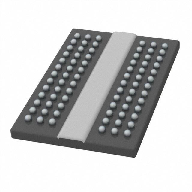


 工商网监
湘ICP备2023018690号
工商网监
湘ICP备2023018690号
