v5.8
ProASICPLUS®
®
Flash Family FPGAs
Features and Benefits
High Performance Routing Hierarchy
•
•
•
•
High Capacity
Commercial and Industrial
•
•
•
I/O
75,000 to 1 Million System Gates
27 k to 198 kbits of Two-Port SRAM
66 to 712 User I/Os
•
•
Military
•
•
•
•
•
•
•
300, 000 to 1 million System Gates
72 k to 198 kbits of Two Port SRAM
158 to 712 User I/Os
Reprogrammable Flash Technology
•
•
•
•
•
•
•
•
•
•
•
•
•
•
Flexibility with Choice of Industry-Standard Front-End Tools
Efficient Design through Front-End Timing and Gate Optimization
ISP Support
•
In-System Programming (ISP) via JTAG Port
SRAMs and FIFOs
•
®
The Industry’s Most Effective Security Key (FlashLock )
•
Low Power
•
•
•
PLL with Flexible Phase, Multiply/Divide and Delay
Capabilities
Internal and/or External Dynamic PLL Configuration
Two LVPECL Differential Pairs for Clock or Data Inputs
Standard FPGA and ASIC Design Flow
3.3 V, 32-Bit PCI, up to 50 MHz (33 MHz over military
temperature)
Two Integrated PLLs
External System Performance up to 150 MHz
Secure Programming
Schmitt-Trigger Option on Every Input
2.5 V/3.3 V Support with Individually-Selectable Voltage and
Slew Rate
Bidirectional Global I/Os
Compliance with PCI Specification Revision 2.2
Boundary-Scan Test IEEE Std. 1149.1 (JTAG) Compliant
Pin Compatible Packages across the ProASICPLUS Family
Unique Clock Conditioning Circuitry
0.22 µm 4 LM Flash-Based CMOS Process
Live At Power-Up (LAPU) Level 0 Support
Single-Chip Solution
No Configuration Device Required
Retains Programmed Design during Power-Down/Up Cycles
Mil/Aero Devices Operate over Full Military Temperature
Range
Performance
•
Ultra-Fast Local and Long-Line Network
High-Speed Very Long-Line Network
High-Performance, Low Skew, Splittable Global Network
100% Routability and Utilization
SmartGen Netlist Generation Ensures Optimal Usage of
Embedded Memory Blocks
24 SRAM and FIFO Configurations with Synchronous and
Asynchronous Operation up to 150 MHz (typical)
Low Impedance Flash Switches
Segmented Hierarchical Routing Structure
Small, Efficient, Configurable (Combinatorial or Sequential)
Logic Cells
Table 1 • ProASICPLUS Product Profile
Device
Maximum System Gates
Tiles (Registers)
Embedded RAM Bits (k=1,024 bits)
Embedded RAM Blocks (256x9)
LVPECL
PLL
Global Networks
Maximum Clocks
Maximum User I/Os
JTAG ISP
PCI
Package (by pin count)
TQFP
PQFP
PBGA
FBGA
CQFP2
CCGA/LGA2
Notes:
APA075
75,000
3,072
27 k
12
2
2
4
24
158
Yes
Yes
APA150
150,000
6,144
36k
16
2
2
4
32
242
Yes
Yes
APA3001
300,000
8,192
72 k
32
2
2
4
32
290
Yes
Yes
APA450
450,000
12,288
108 k
48
2
2
4
48
344
Yes
Yes
APA6001
600,000
21,504
126 k
56
2
2
4
56
454
Yes
Yes
APA750
750,000
32,768
144 k
64
2
2
4
64
562
Yes
Yes
APA10001
1,000,000
56,320
198 k
88
2
2
4
88
712
Yes
Yes
100, 144
208
–
144
100
208
456
144, 256
–
208
456
144, 256
208, 352
–
208
456
144, 256, 484
–
208
456
256, 484, 676
208, 352
624
–
208
456
676, 896
–
208
456
896, 1152
208, 352
624
1. Available as Commercial/Industrial and Military/MIL-STD-883B devices.
2. These packages are available only for Military/MIL-STD-883B devices.
June 2009
© 2009 Actel Corporation
i
See the Actel website for the latest version of the datasheet.
�ProASICPLUS Flash Family FPGAs
Ordering Information
APA1000
_
F
FG
G
1152
I
Application (Ambient Temperature Range)
Blank = Commercial (0˚C to +70˚C)
I = Industrial (-40˚C to +85˚C)
PP = Pre-production
ES = Engineering Silicon (Room Temperature Only)
M = Military (-55˚C to 125˚C)
B = MIL-STD-883 Class B
Package Lead Count
Lead-free packaging
Blank = Standard Packaging
G = RoHS Compliant Packaging
Package Type
TQ = Thin Quad Flat Pack (0.5 mm pitch)
PQ = Plastic Quad Flat Pack (0.5 mm pitch)
FG = Fine Pitch Ball Grid Array (1.0 mm pitch)
BG = Plastic Ball Grid Array (1.27 mm pitch)
CQ = Ceramic Quad Flat Pack (1.05 mm pitch)
CG = Ceramic Column Grid Array (1.27 mm pitch)
LG = Land Grid Array (1.27 mm pitch)
Speed Grade
Blank = Standard Speed
F = 20% Slower than Standard
Part Number
APA075
APA150
APA300
APA450
APA600
APA750
APA1000
ii
=
=
=
=
=
=
=
75,000 Equivalent System Gates
150,000 Equivalent System Gates
300,000 Equivalent System Gates
450,000 Equivalent System Gates
600,000 Equivalent System Gates
750,000 Equivalent System Gates
1,000,000 Equivalent System Gates
v5.8
�ProASICPLUS Flash Family FPGAs
Device Resources
User I/Os2
Military/MIL-STD-883B
Commercial/Industrial
Device
CCGA/
LGA
TQFP
TQFP
PQFP
PBGA FBGA FBGA FBGA FBGA FBGA
FBGA
CQFP
CQFP
100-Pin 144-Pin 208-Pin 456-Pin 144-Pin 256-Pin 484-Pin 676-Pin 896-Pin 1152-Pin 208-Pin 352-Pin 624-Pin
APA075
66
APA150
66
APA300
APA450
APA600
107
158
100
158
242
100
186 3
158 4
290 4
100 4
186 3, 4
158
158
4
344
356
4
APA750
158
356
APA1000
158 4
356 4
100
186
186
3
344
3, 4
158
248
158
248
440
158
248
440
3
370 3
454
454
562 5
642 4, 5
712 5
Notes:
1. Package Definitions: TQFP = Thin Quad Flat Pack, PQFP = Plastic Quad Flat Pack, PBGA = Plastic Ball Grid Array, FBGA = Fine Pitch Ball Grid
Array, CQFP = Ceramic Quad Flat Pack, CCGA = Ceramic Column Grid Array, LGA = Land Grid Array
2. Each pair of PECL I/Os is counted as one user I/O.
3. FG256 and FG484 are footprint-compatible packages.
4. Military Temperature Plastic Package Offering
5. FG896 and FG1152 are footprint-compatible packages.
General Guideline
Maximum performance numbers in this datasheet are based on characterized data. Actel does not guarantee
performance beyond the limits specified within the datasheet.
v5.8
iii
�ProASICPLUS Flash Family FPGAs
Temperature Grade Offerings
Package
APA075
APA150
TQ100
C, I
C, I
TQ144
C, I
PQ208
C, I
BG456
FG144
FG256
C, I
APA300
APA450
APA600
APA750
APA1000
C, I
C, I, M
C, I
C, I, M
C, I
C, I, M
C, I
C, I, M
C, I
C, I, M
C, I
C, I, M
C, I
C, I, M
C, I
C, I
C, I, M
C, I
C, I, M
C, I
C, I, M
FG484
FG676
C, I, M
FG896
C, I
C, I
FG1152
C, I, M
C, I
CQ208
M, B
M, B
M, B
CQ352
M, B
M, B
M, B
M, B
M, B
CG624
Note: C = Commercial
I = Industrial
M = Military
B = MIL-STD-883
Speed Grade and Temperature Matrix
C
–F
Std.
✓
✓
I
✓
M, B
✓
Note: C = Commercial
I = Industrial
M = Military
B = MIL-STD-883
iv
v5.8
�ProASICPLUS Flash Family FPGAs
Table of Contents
General Description
ProASICPLUS Architecture . . . . . . . . . . . . . . . . . . . . . . . . . . . . . . . . . . . . . . . . . . . . . 1-2
Timing Control and Characteristics . . . . . . . . . . . . . . . . . . . . . . . . . . . . . . . . . . . . . 1-13
Sample Implementations . . . . . . . . . . . . . . . . . . . . . . . . . . . . . . . . . . . . . . . . . . . . . 1-16
Adjustable Clock Delay . . . . . . . . . . . . . . . . . . . . . . . . . . . . . . . . . . . . . . . . . . . . . . . 1-16
Clock Skew Minimization . . . . . . . . . . . . . . . . . . . . . . . . . . . . . . . . . . . . . . . . . . . . . 1-16
PLL Electrical Specifications . . . . . . . . . . . . . . . . . . . . . . . . . . . . . . . . . . . . . . . . . . . 1-21
Design Environment . . . . . . . . . . . . . . . . . . . . . . . . . . . . . . . . . . . . . . . . . . . . . . . . . 1-28
ISP . . . . . . . . . . . . . . . . . . . . . . . . . . . . . . . . . . . . . . . . . . . . . . . . . . . . . . . . . . . . . . . 1-28
Related Documents . . . . . . . . . . . . . . . . . . . . . . . . . . . . . . . . . . . . . . . . . . . . . . . . . 1-29
Package Thermal Characteristics . . . . . . . . . . . . . . . . . . . . . . . . . . . . . . . . . . . . . . . 1-30
Calculating Typical Power Dissipation . . . . . . . . . . . . . . . . . . . . . . . . . . . . . . . . . . . 1-31
Operating Conditions . . . . . . . . . . . . . . . . . . . . . . . . . . . . . . . . . . . . . . . . . . . . . . . . 1-34
Tristate Buffer Delays . . . . . . . . . . . . . . . . . . . . . . . . . . . . . . . . . . . . . . . . . . . . . . . . 1-45
Output Buffer Delays . . . . . . . . . . . . . . . . . . . . . . . . . . . . . . . . . . . . . . . . . . . . . . . .
Input Buffer Delays . . . . . . . . . . . . . . . . . . . . . . . . . . . . . . . . . . . . . . . . . . . . . . . . . .
Global Input Buffer Delays . . . . . . . . . . . . . . . . . . . . . . . . . . . . . . . . . . . . . . . . . . . .
Predicted Global Routing Delay . . . . . . . . . . . . . . . . . . . . . . . . . . . . . . . . . . . . . . .
1-47
1-49
1-51
1-53
Global Routing Skew . . . . . . . . . . . . . . . . . . . . . . . . . . . . . . . . . . . . . . . . . . . . . . . . 1-53
Module Delays . . . . . . . . . . . . . . . . . . . . . . . . . . . . . . . . . . . . . . . . . . . . . . . . . . . . . 1-54
Sample Macrocell Library Listing . . . . . . . . . . . . . . . . . . . . . . . . . . . . . . . . . . . . . . . 1-54
Embedded Memory Specifications . . . . . . . . . . . . . . . . . . . . . . . . . . . . . . . . . . . . . 1-57
Pin Description . . . . . . . . . . . . . . . . . . . . . . . . . . . . . . . . . . . . . . . . . . . . . . . . . . . . . 1-76
Recommended Design Practice for VPN/VPP . . . . . . . . . . . . . . . . . . . . . . . . . . . . . . 1-77
Package Pin Assignments
100-Pin TQFP . . . . . . . . . . . . . . . . . . . . . . . . . . . . . . . . . . . . . . . . . . . . . . . . . . . . . . . . 2-1
144-Pin TQFP . . . . . . . . . . . . . . . . . . . . . . . . . . . . . . . . . . . . . . . . . . . . . . . . . . . . . . . . 2-3
208-Pin PQFP . . . . . . . . . . . . . . . . . . . . . . . . . . . . . . . . . . . . . . . . . . . . . . . . . . . . . . . . 2-5
208-Pin CQFP . . . . . . . . . . . . . . . . . . . . . . . . . . . . . . . . . . . . . . . . . . . . . . . . . . . . . . . 2-12
352-Pin CQFP . . . . . . . . . . . . . . . . . . . . . . . . . . . . . . . . . . . . . . . . . . . . . . . . . . . . . . . 2-16
456-Pin PBGA . . . . . . . . . . . . . . . . . . . . . . . . . . . . . . . . . . . . . . . . . . . . . . . . . . . . . . 2-22
144-Pin FBGA . . . . . . . . . . . . . . . . . . . . . . . . . . . . . . . . . . . . . . . . . . . . . . . . . . . . . . 2-37
256-Pin FBGA . . . . . . . . . . . . . . . . . . . . . . . . . . . . . . . . . . . . . . . . . . . . . . . . . . . . . . 2-40
484-Pin FBGA . . . . . . . . . . . . . . . . . . . . . . . . . . . . . . . . . . . . . . . . . . . . . . . . . . . . . . 2-45
676-Pin FBGA . . . . . . . . . . . . . . . . . . . . . . . . . . . . . . . . . . . . . . . . . . . . . . . . . . . . . . 2-51
896-Pin FBGA . . . . . . . . . . . . . . . . . . . . . . . . . . . . . . . . . . . . . . . . . . . . . . . . . . . . . . 2-59
1152-Pin FBGA . . . . . . . . . . . . . . . . . . . . . . . . . . . . . . . . . . . . . . . . . . . . . . . . . . . . . 2-69
624-Pin CCGA/LGA . . . . . . . . . . . . . . . . . . . . . . . . . . . . . . . . . . . . . . . . . . . . . . . . . . 2-78
Datasheet Information
List of Changes . . . . . . . . . . . . . . . . . . . . . . . . . . . . . . . . . . . . . . . . . . . . . . . . . . . . . . 3-1
Data Sheet Categories . . . . . . . . . . . . . . . . . . . . . . . . . . . . . . . . . . . . . . . . . . . . . . . . 3-8
Export Administration Regulations (EAR) . . . . . . . . . . . . . . . . . . . . . . . . . . . . . . . . . 3-8
Actel Safety Critical, Life Support, and High-Reliability Applications Policy . . . . . 3-8
v5.8
v
��ProASICPLUS Flash Family FPGAs
General Description
The ProASICPLUS family of devices, Actel’s secondgeneration Flash FPGAs, offers enhanced performance
over Actel’s ProASIC family. It combines the advantages
of ASICs with the benefits of programmable devices
through nonvolatile Flash technology. This enables
engineers to create high-density systems using existing
ASIC or FPGA design flows and tools. In addition, the
ProASICPLUS family offers a unique clock conditioning
circuit based on two on-board phase-locked loops (PLLs).
The family offers up to one million system gates,
supported with up to 198 kbits of two-port SRAM and up
to 712 user I/Os, all providing 50 MHz PCI performance.
combination of fine granularity, flexible routing
resources, and abundant Flash switches allow 100%
utilization and over 95% routability for highly congested
designs. Tiles and larger functions are interconnected
through a four-level routing hierarchy.
Embedded two-port SRAM blocks with built-in FIFO/RAM
control logic can have user-defined depths and widths.
Users can also select programming for synchronous or
asynchronous operation, as well as parity generations or
checking.
Advantages
to
the
designer
extend
beyond
performance. Unlike SRAM-based FPGAs, four levels of
routing hierarchy simplify routing, while the use of Flash
technology allows all functionality to be live at powerup. No external boot PROM is required to support device
programming. While on-board security mechanisms
prevent
access
to
the
program
information,
reprogramming can be performed in-system to support
future design iterations and field upgrades. The device’s
architecture mitigates the complexity of ASIC migration
at higher user volume. This makes ProASICPLUS a costeffective solution for applications in the networking,
communications, computing, and avionics markets.
The unique clock conditioning circuitry in each device
includes two clock conditioning blocks. Each block
provides a PLL core, delay lines, phase shifts (0° and
180°), and clock multipliers/dividers, as well as the
circuitry needed to provide bidirectional access to the
PLL. The PLL block contains four programmable
frequency dividers which allow the incoming clock signal
to be divided by a wide range of factors from 1 to 64.
The clock conditioning circuit also delays or advances the
incoming reference clock up to 8 ns (in increments of
0.25 ns). The PLL can be configured internally or
externally during operation without redesigning or
reprogramming the part. In addition to the PLL, there
are two LVPECL differential input pairs to accommodate
high-speed clock and data inputs.
The ProASICPLUS family achieves its nonvolatility and
reprogrammability through an advanced Flash-based
0.22 μm LVCMOS process with four layers of metal.
Standard CMOS design techniques are used to
implement logic and control functions, including the
PLLs and LVPECL inputs. This results in predictable
performance compatible with gate arrays.
To support customer needs for more comprehensive,
lower-cost, board-level testing, Actel’s ProASICPLUS
devices are fully compatible with IEEE Standard 1149.1
for test access port and boundary-scan test architecture.
For more information concerning the Flash FPGA
implementation, please refer to the "Boundary Scan
(JTAG)" section on page 1-11.
The ProASICPLUS architecture provides granularity
comparable to gate arrays. The device core consists of a
Sea-of-Tiles™. Each tile can be configured as a flip-flop,
latch, or three-input/one-output logic function by
programming the appropriate Flash switches. The
ProASICPLUS devices are available in a variety of highperformance plastic packages. Those packages and the
performance features discussed above are described in
more detail in the following sections.
v5.8
1-1
�ProASICPLUS Flash Family FPGAs
ProASICPLUS Architecture
The proprietary ProASICPLUS architecture
granularity comparable to gate arrays.
the appropriate logic cell inputs and outputs. Dedicated
high-performance lines are connected as needed for fast,
low-skew global signal distribution throughout the core.
Maximum core utilization is possible for virtually any
design.
provides
The ProASICPLUS device core consists of a Sea-of-Tiles
(Figure 1-1). Each tile can be configured as a three-input
logic function (e.g., NAND gate, D-Flip-Flop, etc.) by
programming
the
appropriate
Flash
switch
interconnections (Figure 1-2 and Figure 1-3 on page 1-3).
Tiles and larger functions are connected with any of the
four levels of routing hierarchy. Flash switches are
distributed throughout the device to provide
nonvolatile, reconfigurable interconnect programming.
Flash switches are programmed to connect signal lines to
ProASICPLUS devices also contain embedded, two-port
SRAM blocks with built-in FIFO/RAM control logic.
Programming
options
include
synchronous
or
asynchronous operation, two-port RAM configurations,
user defined depth and width, and parity generation or
checking. Please see the "Embedded Memory
Configurations" section on page 1-23 for more
information.
RAM Block
256x9 Two-Port SRAM
or FIFO Block
I/Os
Logic Tile
RAM Block
256x9 Two Port SRAM
or FIFO Block
Figure 1-1 • The ProASICPLUS Device Architecture
Floating Gate
Sensing
Switch In
Switching
Word
Switch Out
Figure 1-2 • Flash Switch
1 -2
v5.8
�ProASICPLUS Flash Family FPGAs
Local Routing
In 1
Efficient Long-Line Routing
In 2 (CLK)
In 3 (Reset)
Figure 1-3 • Core Logic Tile
Live at Power-Up
Flash Switch
PLUS
Unlike SRAM FPGAs, ProASICPLUS uses a live-on-power-up
ISP Flash switch as its programming element.
The Actel Flash-based ProASIC
devices support
Level 0 of the live at power-up (LAPU) classification
standard. This feature helps in system component
initialization, executing critical tasks before the
processor wakes up, setting up and configuring memory
blocks, clock generation, and bus activity management.
The LAPU feature of Flash-based ProASICPLUS devices
greatly simplifies total system design and reduces total
system cost, often eliminating the need for Complex
Programmable Logic Device (CPLD) and clock generation
PLLs that are used for this purpose in a system. In
addition, glitches and brownouts in system power will
not corrupt the ProASICPLUS device's Flash configuration,
and unlike SRAM-based FPGAs, the device will not have
to be reloaded when system power is restored. This
enables the reduction or complete removal of the
configuration PROM, expensive voltage monitor,
brownout detection, and clock generator devices from
the PCB design. Flash-based ProASICPLUS devices simplify
total system design, and reduce cost and design risk,
while increasing system reliability and improving system
initialization time.
In the ProASICPLUS Flash switch, two transistors share the
floating gate, which stores the programming
information. One is the sensing transistor, which is only
used for writing and verification of the floating gate
voltage. The other is the switching transistor. It can be
used in the architecture to connect/separate routing nets
or to configure logic. It is also used to erase the floating
gate (Figure 1-2 on page 1-2).
Logic Tile
The logic tile cell (Figure 1-3) has three inputs (any or all
of which can be inverted) and one output (which can
connect to both ultra-fast local and efficient long-line
routing resources). Any three-input, one-output logic
function (except a three-input XOR) can be configured as
one tile. The tile can be configured as a latch with clear
or set or as a flip-flop with clear or set. Thus, the tiles can
flexibly map logic and sequential gates of a design.
v5.8
1-3
�ProASICPLUS Flash Family FPGAs
Routing Resources
The routing structure of ProASICPLUS devices is designed
to provide high performance through a flexible fourlevel hierarchy of routing resources: ultra-fast local
resources, efficient long-line resources, high-speed, very
long-line resources, and high performance global
networks.
can in turn access every input of every tile. Active buffers
are inserted automatically by routing software to limit
the loading effects due to distance and fanout.
The ultra-fast local resources are dedicated lines that
allow the output of each tile to connect directly to every
input of the eight surrounding tiles (Figure 1-4).
The high-performance global networks are low-skew,
high fanout nets that are accessible from external pins or
from internal logic (Figure 1-7 on page 1-7). These nets
are typically used to distribute clocks, resets, and other
high fanout nets requiring a minimum skew. The global
networks are implemented as clock trees, and signals can
be introduced at any junction. These can be employed
hierarchically with signals accessing every input on all
tiles.
The efficient long-line resources provide routing for
longer distances and higher fanout connections. These
resources vary in length (spanning 1, 2, or 4 tiles), run
both vertically and horizontally, and cover the entire
ProASICPLUS device (Figure 1-5 on page 1-5). Each tile can
drive signals onto the efficient long-line resources, which
L
Inputs
L
L
L
L
Ultra-Fast
Local Lines
(connects a tile to the
adjacent tile, I/O buffer,
or memory block)
Output
L
The high-speed, very long-line resources, which span the
entire device with minimal delay, are used to route very
long or very high fanout nets. (Figure 1-6 on page 1-6).
L
L
L
Figure 1-4 • Ultra-Fast Local Resources
1 -4
v5.8
�ProASICPLUS Flash Family FPGAs
Spans 1 Tile
Spans 2 Tiles
Spans 4 Tiles
Logic Tile
L
L
L
L
L
L
L
L
L
L
L
L
L
L
L
L
L
L
L
L
L
L
L
L
Spans 1 Tile
Spans 2 Tiles
Spans 4 Tiles
Logic Cell
L
L
L
L
L
L
Figure 1-5 • Efficient Long-Line Resources
v5.8
1-5
�ProASICPLUS Flash Family FPGAs
High Speed Very Long-Line Resouces
PAD RING
I/O RING
I/O RING
PAD RING
SRAM
SRAM
PAD RING
Figure 1-6 • High-Speed, Very Long-Line Resources
Clock Resources
Clock Trees
ProASICPLUS
The
family offers powerful and flexible
control of circuit timing through the use of analog
circuitry. Each chip has two clock conditioning blocks
containing a phase-locked loop (PLL) core, delay lines,
phase shifter (0° and 180°), clock multiplier/dividers, and
all the circuitry needed for the selection and
interconnection of inputs to the global network (thus
providing bidirectional access to the PLL). This permits
the PLL block to drive inputs and/or outputs via the two
global lines on each side of the chip (four total lines).
This circuitry is discussed in more detail in the
"ProASICPLUS Clock Management System" section on
page 1-13.
1 -6
v5.8
One of the main architectural benefits of ProASICPLUS is
the set of power- and delay-friendly global networks.
ProASICPLUS offers four global trees. Each of these trees
is based on a network of spines and ribs that reach all
the tiles in their regions (Figure 1-7 on page 1-7). This
flexible clock tree architecture allows users to map up to
88 different internal/external clocks in an APA1000
device. Details on the clock spines and various numbers
of the family are given in Table 1-1 on page 1-7.
The flexible use of the ProASICPLUS clock spine allows the
designer to cope with several design requirements. Users
implementing clock-resource intensive applications can
easily route external or gated internal clocks using global
routing spines. Users can also drastically reduce delay
penalties and save buffering resources by mapping
critical high fanout nets to spines. For design hints on
using these features, refer to Actel’s Efficient Use of
ProASIC Clock Trees application note.
�ProASICPLUS Flash Family FPGAs
High-Performance
Global Network
I/O RING
PAD RING
PAD RING
Top Spine
Global Networks
Global
Pads
Global
Pads
Global Spine
I/O RING
Global Ribs
Bottom Spine
Scope of Spine
(Shaded area
plus local RAMs
and I/Os)
PAD RING
Note: This figure shows routing for only one global path.
Figure 1-7 • High-Performance Global Network
Table 1-1 •
Clock Spines
APA075
APA150
APA300
APA450
APA600
APA750
APA1000
Global Clock Networks (Trees)
4
4
4
4
4
4
4
Clock Spines/Tree
6
8
8
12
14
16
22
Total Spines
24
32
32
48
56
64
88
Top or Bottom Spine Height (Tiles)
16
24
32
32
48
64
80
Tiles in Each Top or Bottom Spine
Total Tiles
512
768
1,024
1,024
1,536
2,048
2,560
3,072
6,144
8,192
12,288
21,504
32,768
56,320
v5.8
1-7
�ProASICPLUS Flash Family FPGAs
Array Coordinates
During many place-and-route operations in Actel’s
Designer software tool, it is possible to set constraints
that require array coordinates.
cells and core cells. In addition, the I/O coordinate system
changes depending on the die/package combination.
Core cell coordinates start at the lower left corner
(represented as (1,1)) or at (1,5) if memory blocks are
present at the bottom. Memory coordinates use the
same system and are indicated in Table 1-2. The memory
coordinates for an APA1000 are illustrated in Figure 1-8.
For more information on how to use constraints, see the
Designer User’s Guide or online help for ProASICPLUS
software tools.
Table 1-2 is provided as a reference. The array coordinates
are measured from the lower left (0,0). They can be used in
region constraints for specific groups of core cells, I/Os, and
RAM blocks. Wild cards are also allowed.
I/O and cell coordinates are used for placement
constraints. Two coordinate systems are needed because
there is not a one-to-one correspondence between I/O
Table 1-2 •
Array Coordinates
Logic Tile
Min.
Device
x
Memory Rows
Max.
y
x
Bottom
Top
y
y
y
All
Min.
Max.
APA075
1
1
96
32
–
(33,33) or (33, 35)
0,0
97, 37
APA150
1
1
128
48
–
(49,49) or (49, 51)
0,0
129, 53
APA300
1
5
128
68
(1,1) or (1,3)
(69,69) or (69, 71)
0,0
129, 73
APA450
1
5
192
68
(1,1) or (1,3)
(69,69) or (69, 71)
0,0
193, 73
APA600
1
5
224
100
(1,1) or (1,3)
(101,101) or (101, 103)
0,0
225, 105
APA750
1
5
256
132
(1,1) or (1,3)
(133,133) or (133, 135)
0,0
257, 137
APA1000
1
5
352
164
(1,1) or (1,3)
(165,165) or (165, 167)
0,0
353, 169
(1,169)
Memory
Blocks
(353,169)
(1,167)
(352,167)
(1,165)
(352,165)
(1,164)
(352,164)
Core
(1,5)
(352,5)
(1,3)
(352,3)
(1,1)
(352,1)
(0,0)
Memory
Blocks
Figure 1-8 • Core Cell Coordinates for the APA1000
1 -8
v5.8
(353,0)
�ProASICPLUS Flash Family FPGAs
Input/Output Blocks
Table 1-3 •
ProASICPLUS I/O Power Supply Voltages
VDDP
To meet complex system demands, the ProASICPLUS
family offers devices with a large number of user I/O
pins, up to 712 on the APA1000. Table 1-3 shows the
available supply voltage configurations (the PLL block
uses an independent 2.5 V supply on the AVDD and
AGND pins). All I/Os include ESD protection circuits. Each
I/O has been tested to 2000 V to the human body model
(per JESD22 (HBM)).
2.5 V
3.3 V
Input Compatibility
2.5 V
3.3 V
Output Drive
2.5 V
3.3 V
3.3V/2.5V
Signal Control
Six or seven standard I/O pads are grouped with a GND
pad and either a VDD (core power) or VDDP (I/O power)
pad. Two reference bias signals circle the chip. One
protects the cascaded output drivers, while the other
creates a virtual VDD supply for the I/O ring.
Y
Pull-up
Control
EN
I/O pads are fully configurable to provide the maximum
flexibility and speed. Each pad can be configured as an
input, an output, a tristate driver, or a bidirectional
buffer (Figure 1-9 and Table 1-4).
A
Pad
3.3 V/2.5 V Signal Control Drive
Strength and Slew-Rate Control
Figure 1-9 • I/O Block Schematic Representation
Table 1-4 •
I/O Features
Function
I/O pads configured as inputs
I/O pads configured as outputs
Description
•
Selectable 2.5 V or 3.3 V threshold levels
•
Optional pull-up resistor
•
Optionally configurable as Schmitt trigger input. The Schmitt trigger input option can be
configured as an input only, not a bidirectional buffer. This input type may be slower than
a standard input under certain conditions and has a typical hysteresis of 0.35 V. I/O macros
with an “S” in the standard I/O library have added Schmitt capabilities.
•
3.3 V PCI Compliant (except Schmitt trigger inputs)
•
Selectable 2.5 V or 3.3 V compliant output signals
•
2.5 V – JEDEC JESD 8-5
•
3.3 V – JEDEC JESD 8-A (LVTTL and LVCMOS)
•
3.3 V PCI compliant
•
Ability to drive LVTTL and LVCMOS levels
•
Selectable drive strengths
•
Selectable slew rates
•
I/O pads configured as bidirectional •
buffers
•
Tristate
Selectable 2.5 V or 3.3 V compliant output signals
2.5 V – JEDEC JESD 8-5
•
3.3 V – JEDEC JESD 8-A (LVTTL and LVCMOS)
•
3.3 V PCI compliant
•
Optional pull-up resistor
•
Selectable drive strengths
•
Selectable slew rates
•
Tristate
v5.8
1-9
�ProASICPLUS Flash Family FPGAs
Power-Up Sequencing
low voltage differential amplifier) and a signal and its
complement, PPECL (I/P) (PECLN) and NPECL (PECLREF).
The LVPECL input pad cell differs from the standard I/O
cell in that it is operated from VDD only.
While ProASICPLUS devices are live at power-up, the order
of VDD and VDDP power-up is important during system
start-up. VDD should be powered up simultaneously with
VDDP on ProASICPLUS devices. Failure to follow these
guidelines may result in undesirable pin behavior during
system start-up. For more information, refer to Actel’s
Power-Up Behavior of ProASICPLUS Devices application
note.
Since it is exclusively an input, it requires no output
signal, output enable signal, or output configuration
bits. As a special high-speed differential input, it also
does not require pull ups. Recommended termination for
LVPECL inputs is shown in Figure 1-10. The LVPECL pad
cell compares voltages on the PPECL (I/P) pad (as
illustrated in Figure 1-11) and the NPECL pad and sends
the results to the global MUX (Figure 1-14 on page 1-14).
This high-speed, low-skew output essentially controls the
clock conditioning circuit.
LVPECL Input Pads
In addition to standard I/O pads and power pads,
ProASICPLUS devices have a single LVPECL input pad on
both the east and west sides of the device, along with
AVDD and AGND pins to power the PLL block. The
LVPECL pad cell consists of an input buffer (containing a
LVPECLs are designed to meet LVPECL JEDEC receiver
standard levels (Table 1-5).
Z 0= 50 Ω
PPECL
+
R = 100 Ω
From LVPECL Driver
Z 0= 50 Ω
Data
_
NPECL
Figure 1-10 • Recommended Termination for LVPECL Inputs
Voltage
2.72
2.125
1.49
0.86
Figure 1-11 • LVPECL High and Low Threshold Values
Table 1-5 •
Symbol
LVPECL Receiver Specifications
Parameter
Min.
Max
Units
VIH
Input High Voltage
1.49
2.72
V
VIL
Input Low Voltage
0.86
2.125
V
VID
Differential Input Voltage
0.3
VDD
V
1 -1 0
v5.8
�ProASICPLUS Flash Family FPGAs
Boundary Scan (JTAG)
pins are dedicated for boundary-scan test usage. Actel
recommends that a nominal 20 kΩ pull-up resistor is
added to TDO and TCK pins.
ProASICPLUS devices are compatible with IEEE Standard
1149.1, which defines a set of hardware architecture and
mechanisms for cost-effective, board-level testing. The
basic ProASICPLUS boundary-scan logic circuit is composed
of the TAP (test access port), TAP controller, test data
registers, and instruction register (Figure 1-12). This
circuit supports all mandatory IEEE 1149.1 instructions
(EXTEST, SAMPLE/PRELOAD and BYPASS) and the
optional IDCODE instruction (Table 1-6).
The TAP controller is a four-bit state machine (16 states)
that operates as shown in Figure 1-13 on page 1-12. The
’1’s and ‘0’s represent the values that must be present at
TMS at a rising edge of TCK for the given state transition
to occur. IR and DR indicate that the instruction register
or the data register is operating in that state.
ProASICPLUS devices have to be programmed at least
once for complete boundary-scan functionality to be
available. Prior to being programmed, EXTEST is not
available. If boundary-scan functionality is required prior
to programming, refer to online technical support on the
Actel website and search for ProASICPLUS BSDL.
Each test section is accessed through the TAP, which has
five associated pins: TCK (test clock input), TDI and TDO
(test data input and output), TMS (test mode selector)
and TRST (test reset input). TMS, TDI and TRST are
equipped with pull-up resistors to ensure proper
operation when no input data is supplied to them. These
I/O
I/O
I/O
I/O
I/O
TDI
Test Data
Registers
Instruction
Register
TAP
Controller
Device
Logic
TDO
I/O
TRST
I/O
TMS
I/O
TCK
I/O
Bypass Register
I/O
I/O
I/O
I/O
I/O
Figure 1-12 • ProASICPLUS JTAG Boundary Scan Test Logic Circuit
Table 1-6 •
Table 1-6 •
Boundary-Scan Opcodes
Boundary-Scan Opcodes
Hex Opcode
Hex Opcode
EXTEST
00
CLAMP
05
SAMPLE/PRELOAD
01
BYPASS
FF
IDCODE
0F
v5.8
1-11
�ProASICPLUS Flash Family FPGAs
The TAP controller receives two control inputs (TMS and
TCK) and generates control and clock signals for the rest
of the test logic architecture. On power-up, the TAP
controller enters the Test-Logic-Reset state. To guarantee
a reset of the controller from any of the possible states,
TMS must remain high for five TCK cycles. The TRST pin
may also be used to asynchronously place the TAP
controller in the Test-Logic-Reset state.
with four fields (lowest significant byte (LSB), ID number,
part number and version). The boundary-scan register
observes and controls the state of each I/O pin.
Each I/O cell has three boundary-scan register cells, each
with a serial-in, serial-out, parallel-in, and parallel-out
pin. The serial pins are used to serially connect all the
boundary-scan register cells in a device into a boundaryscan register chain, which starts at the TDI pin and ends
at the TDO pin. The parallel ports are connected to the
internal core logic tile and the input, output, and control
ports of an I/O buffer to capture and load data into the
register to control or observe the logic state of each I/O.
ProASICPLUS devices support three types of test data
registers: bypass, device identification, and boundary
scan. The bypass register is selected when no other
register needs to be accessed in a device. This speeds up
test data transfer to other devices in a test data path.
The 32-bit device identification register is a shift register
1
Test-Logic
Reset
0
0
Run-Test/
Idle
1
1
Select-DRScan
0
Capture-DR
1
Capture-IR
1
0
0
0
Shift-DR
0
0
1
1
Exit-IR
0
1
1
Exit2-DR
1
Update-DR
0
1
Figure 1-13 • TAP Controller State Diagram
1 -1 2
v5.8
0
Pause-IR
Pause-DR
0
0
Shift-IR
1
Exit-DR
1
Select-IRScan
0
0
Exit2-IR
1
Update-IR
0
1
1
�ProASICPLUS Flash Family FPGAs
Timing Control and
Characteristics
ProASICPLUS
follows (Figure 1-15 on page 1-15, Table 1-7 on page 115, and Table 1-8 on page 1-16):
Global A (secondary clock)
•
•
Clock Management System
ProASICPLUS devices provide designers with very flexible
clock conditioning capabilities. Each member of the
ProASICPLUS family contains two phase-locked loop (PLL)
blocks which perform the following functions:
•
Clock Phase Adjustment via Programmable Delay
(250 ps steps from –7 ns to +8 ns)
•
Clock Skew Minimization
•
Clock Frequency Synthesis
•
•
Output from Global MUX A
Conditioned version of PLL output (fOUT) – delayed
or advanced
Divided version of either of the above
Further delayed version of either of the above
(0.25 ns, 0.50 ns, or 4.00 ns delay)1
Global B
•
•
•
•
Each PLL has the following key features:
Output from Global MUX B
Delayed or advanced version of fOUT
Divided version of either of the above
Further delayed version of either of the above
(0.25 ns, 0.50 ns, or 4.00 ns delay)2
•
Input Frequency Range (fIN) = 1.5 to 180 MHz
•
Feedback Frequency Range (fVCO) = 24 to 180 MHz
•
Output Frequency Range (fOUT) = 8 to 180 MHz
Functional Description
•
Output Phase Shift = 0 ° and 180 °
•
Output Duty Cycle = 50%
•
Low Output Jitter (max at 25°C)
Each PLL block contains four programmable dividers as
shown in Figure 1-14 on page 1-14. These allow
frequency scaling of the input clock signal as follows:
–
fVCO 60 MHz. Jitter ±1% or better
•
•
Note: Jitter(ps) = Jitter(%)* period
•
For Example:
Jitter in picoseconds at 100 MHz = 0.01 * (1/100E6) = 100 ps
•
•
Maximum Acquisition = 80 µs for fVCO > 40 MHz
Time
= 30 µs for fVCO < 40 MHz
•
Low Power Consumption – 6.9 mW (max – analog
supply) + 7.0μW/MHz (max – digital supply)
The n divider divides the input clock by integer
factors from 1 to 32.
The m divider in the feedback path allows
multiplication of the input clock by integer factors
ranging from 1 to 64.
The two dividers together can implement any
combination of multiplication and division
resulting in a clock frequency between 24 and 180
MHz exiting the PLL core. This clock has a fixed
50% duty cycle.
The output frequency of the PLL core is given by
the formula EQ 1-1 (fREF is the reference clock
frequency):
fOUT = fREF * m/n
EQ 1-1
Physical Implementation
•
Each side of the chip contains a clock conditioning circuit
based on a 180 MHz PLL block (Figure 1-14 on page 114). Two global multiplexed lines extend along each side
of the chip to provide bidirectional access to the PLL on
that side (neither MUX can be connected to the opposite
side's PLL). Each global line has optional LVPECL input
pads (described below). The global lines may be driven
by either the LVPECL global input pad or the outputs
from the PLL block, or both. Each global line can be
driven by a different output from the PLL. Unused global
pins can be configured as regular I/Os or left
unconnected. They default to an input with pull-up. The
two signals available to drive the global networks are as
The third and fourth dividers (u and v) permit the
signals applied to the global network to each be
further divided by integer factors ranging from 1
to 4.
The implementations shown in EQ2 and EQ3 enable the
user to define a wide range of frequency multiplier and
divisors.
fGLB = m/(n*u)
EQ 1-2
fGLA = m/(n*v)
EQ 1-3
1. This mode is available through the delay feature of the Global MUX driver.
v5.8
1-13
�ProASICPLUS Flash Family FPGAs
enable the user to define a wide range of frequency
multipliers and divisors. The clock conditioning circuit can
advance or delay the clock up to 8 ns (in increments of
0.25 ns) relative to the positive edge of the incoming
reference clock. The system also allows for the selection of
output frequency clock phases of 0° and 180°.
signals relative to other signals to assist in the control of
input set-up times. Not all possible combinations of input
and output modes can be used. The degrees of freedom
available in the bidirectional global pad system and in
the clock conditioning circuit have been restricted. This
avoids unnecessary and unwieldy design kit and software
work.
Prior to the application of signals to the rib drivers, they
pass through programmable delay units, one per global
network. These units permit the delaying of global
AVDD
AGND
VDD
GND
GLA
Global MUX B OUT
Input Pins to the PLL
See Figure 1-15
+ 1-14
on page
-
Clock Conditioning
Circuitry
(Top level view)
External Feedback Signal
GLB
27
4
Global MUX A OUT
8
Flash
Configuration Bits
Dynamic
Configuration Bits
Clock Conditioning Circuitry Detailed Block Diagram
CLK
Bypass Primary
1
P+
FIVDIV[4:0]
P-
7
÷n
PLL Core
180˚
÷m
0˚
FBDIV[5:0]
Clock from Core
(GLINT mode)
6
5
4
0
÷u
DLYB[1:0]
Delay Line 0.0 ns, 0.25 ns,
0.50 ns and 4.00 ns
OBDIV[1:0]
1
1
Delay Line
0.25 ns to
4.00 ns,
16 steps,
0.25 ns
increments
XDLYSEL
Deskew
Delay
2.95 ns
2
3
FBDLY[3:0]
FBSEL[1:0]
3
OADIV[1:0]
2
÷v
DLYA[1:0]
Delay Line 0.0 ns, 0.25 ns,
0.50 ns and 4.00 ns
1
OAMUX[1:0]
CLKA
Bypass Secondary
Clock from Core
(GLINT mode)
Notes:
1. FBDLY is a programmable delay line from 0 to 4 ns in 250 ps increments.
2. DLYA and DLYB are programmable delay lines, each with selectable values 0 ps, 250 ps, 500 ps, and 4 ns.
3. OBDIV will also divide the phase-shift since it takes place after the PLL Core.
Figure 1-14 • PLL Block – Top-Level View and Detailed PLL Block Diagram
1 -1 4
GLB
2
0
EXTFB
OBMUX[2:0]
v5.8
GLA
�ProASICPLUS Flash Family FPGAs
Package Pins
GL
Physical I/O
Buffers
Global MUX
Configuration Tile
Std. Pad Cell
Global MUX B
OUT
NPECL
PECL Pad Cell
PPECL
External
Feedback
GLMX
Std. Pad Cell
GL
Std. Pad Cell
Global MUX A
OUT
Configuration Tile
CORE
Legend
Physical Pin
DATA Signals to the Global MUX
DATA Signals to the Core
Control Signals to the Global MUX
DATA Signals to the PLL Block
Note: When a signal from an I/O tile is connected to the core, it cannot be connected to the Global MUX at the same time.
Figure 1-15 • Input Connectors to ProASICPLUS Clock Conditioning Circuitry
Table 1-7 •
Clock-Conditioning Circuitry MUX Settings
MUX
Datapath
Comments
FBSEL
1
Internal Feedback
2
Internal Feedback and Advance Clock Using FBDLY
3
External Feedback (EXTFB)
–0.25 to –4 ns in 0.25 ns increments
XDLYSEL
0
Feedback Unchanged
1
Deskew feedback by advancing clock by system delay
OBMUX
Fixed delay of -2.95 ns
GLB
0
Primary bypass, no divider
1
Primary bypass, use divider
2
Delay Clock Using FBDLY
4
Phase Shift Clock by 0°
5
Reserved
6
Phase Shift Clock by +180°
7
Reserved
OAMUX
+0.25 to +4 ns in 0.25 ns increments
GLA
0
Secondary bypass, no divider
1
Secondary bypass, use divider
2
Delay Clock Using FBDLY
3
Phase Shift Clock by 0°
+0.25 to +4 ns in 0.25 ns increments
v5.8
1-15
�ProASICPLUS Flash Family FPGAs
Table 1-8 •
Sample Implementations
Clock-Conditioning Circuitry Delay-Line
Settings
Delay Line
Delay Value (ns)
Frequency Synthesis
DLYB
0
0
1
+0.25
2
+0.50
3
+4.0
DLYA
0
0
1
+0.25
2
+0.50
3
+4.0
Lock Signal
An active-high Lock signal (added via the SmartGen PLL
development tool) indicates that the PLL has locked to
the incoming clock signal. The PLL will acquire and
maintain lock even when there is jitter on the incoming
clock signal. The PLL will maintain lock with an input
jitter up to 5% of the input period, with a maximum of
5 ns. Users can employ the Lock signal as a soft reset of
the logic driven by GLB and/or GLA. Note if FIN is not
within specified frequencies, then both the FOUT and lock
signal are indeterminate.
PLL Configuration Options
The PLL can be configured during design (via Flashconfiguration bits set in the programming bitstream) or
dynamically during device operation, thus eliminating
the need to reprogram the device. The dynamic
configuration bits are loaded into a serial-in/parallel-out
shift register provided in the clock conditioning circuit.
The shift register can be accessed either from user logic
within the device or via the JTAG port. Another option is
internal dynamic configuration via user-designed
hardware. Refer to Actel's ProASICPLUS PLL Dynamic
Reconfiguration Using JTAG application note for more
information.
For information on the clock conditioning circuit, refer
to Actel’s Using ProASICPLUS Clock Conditioning Circuits
application note.
1 -1 6
v5.8
Figure 1-16 on page 1-17 illustrates an example where
the PLL is used to multiply a 33 MHz external clock up to
133 MHz. Figure 1-17 on page 1-17 uses two dividers to
synthesize a 50 MHz output clock from a 40 MHz input
reference clock. The input frequency of 40 MHz is
multiplied by five and divided by four, giving an output
clock (GLB) frequency of 50 MHz. When dividers are
used, a given ratio can be generated in multiple ways,
allowing the user to stay within the operating frequency
ranges of the PLL. For example, in this case the input
divider could have been two and the output divider also
two, giving us a division of the input frequency by four
to go with the feedback loop division (effective
multiplication) by five.
Adjustable Clock Delay
Figure 1-18 on page 1-18 illustrates the delay of the
input clock by employing one of the adjustable delay
lines. This is easily done in ProASICPLUS by bypassing the
PLL core entirely and using the output delay line. Notice
also that the output clock can be effectively advanced
relative to the input clock by using the delay line in the
feedback path. This is shown in Figure 1-19 on page 1-18.
Clock Skew Minimization
Figure 1-20 on page 1-19 indicates how feedback from
the clock network can be used to create minimal skew
between the distributed clock network and the input
clock. The input clock is fed to the reference clock input
of the PLL. The output clock (GLA) feeds a clock network.
The feedback input to the PLL uses a clock input delayed
by a routing network. The PLL then adjusts the phase of
the input clock to match the delayed clock, thus
providing nearly zero effective skew between the two
clocks. Refer to Actel's Using ProASICPLUS Clock
Conditioning Circuits application note for more
information.
�ProASICPLUS Flash Family FPGAs
Global MUX B OUT
33 MHz
÷1
÷n
180˚
PLL Core
0˚
÷m
÷4
÷u
÷1
D
GLB
133 MHz
D
D
External Feedback
÷v
D
GLA
Global MUX A OUT
Figure 1-16 • Using the PLL 33 MHz In, 133 MHz Out
Global MUX B OUT
40 MHz
÷4
÷n
180˚
PLL Core
÷m
0˚
÷u
÷1
GLB
D
50 MHz
÷5
D
D
External Feedback
÷v
D
GLA
Global MUX A OUT
Figure 1-17 • Using the PLL 40 MHz In, 50 MHz Out
v5.8
1-17
�ProASICPLUS Flash Family FPGAs
Global MUX B OUT
133 MHz
÷1
÷n
180˚
PLL Core
÷m
0˚
÷1
÷u
÷1
GLB
D
133 MHz
D
D
External Feedback
÷v
D
GLA
Global MUX A OUT
Figure 1-18 • Using the PLL to Delay the Input Clock
Global MUX B OUT
133 MHz
÷1
÷n
180˚
PLL Core
0˚
÷m
÷u
÷1
GLB
D
133 MHz
÷1
D
D
External Feedback
÷v
Global MUX A OUT
Figure 1-19 • Using the PLL to Advance the Input Clock
1 -1 8
v5.8
D
GLA
�ProASICPLUS Flash Family FPGAs
Off chip
Global MUX B
OUT
On chip
/1
180˚
÷n
133 MHz
PLL Core
0˚
÷m
÷u
D
GL
B
/1
D
External
Feedback
D
133 MHz
÷v
Global MUX A
OUT
Reference
clock
Q
SET
D
GL
A
D
Q CLR
Figure 1-20 • Using the PLL for Clock Deskewing
v5.8
1-19
�ProASICPLUS Flash Family FPGAs
Logic Tile Timing Characteristics
Timing Derating
ProASICPLUS
Timing characteristics for
devices fall into
three categories: family dependent, device dependent,
and design dependent. The input and output buffer
characteristics are common to all ProASICPLUS family
members. Internal routing delays are device dependent.
Design dependency means that actual delays are not
determined until after placement and routing of the
user’s design are complete. Delay values may then be
determined by using the Timer utility or by performing
simulation with post-layout delays.
Since ProASICPLUS devices are manufactured with a
CMOS process, device performance will vary with
temperature, voltage, and process. Minimum timing
parameters reflect maximum operating voltage,
minimum operating temperature, and optimal process
variations. Maximum timing parameters reflect minimum
operating voltage, maximum operating temperature,
and worst-case process variations (within process
specifications). The derating factors shown in Table 1-9
should be applied to all timing data contained within
this datasheet.
Critical Nets and Typical Nets
All timing numbers listed in this datasheet represent
sample timing characteristics of ProASICPLUS devices.
Actual timing delay values are design-specific and can be
derived from the Timer tool in Actel’s Designer software
after place-and-route.
Propagation delays are expressed only for typical nets,
which are used for initial design performance evaluation.
Critical net delays can then be applied to the most
timing-critical paths. Critical nets are determined by net
property assignment prior to place-and-route. Refer to
the Actel Designer User’s Guide or online help for details
on using constraints.
Table 1-9 •
Temperature and Voltage Derating Factors
(Normalized to Worst-Case Commercial, TJ = 70°C, VDD = 2.3 V)
–55°C
–40°C
0°C
25°C
70°C
85°C
110°C
125°C
135°C
150°C
2.3 V
0.84
0.86
0.91
0.94
1.00
1.02
1.05
1.13
1.18
1.27
2.5 V
0.81
0.82
0.87
0.90
0.95
0.98
1.01
1.09
1.13
1.21
2.7 V
0.77
0.79
0.83
0.86
0.91
0.93
0.96
1.04
1.08
1.16
Notes:
1. The user can set the junction temperature in Designer software to be any integer value in the range of –55°C to 175°C.
2. The user can set the core voltage in Designer software to be any value between 1.4 V and 1.6 V.
1 -2 0
v5.8
�ProASICPLUS Flash Family FPGAs
PLL Electrical Specifications
Parameter
Value TJ ≤ –40°C
Value TJ > –40°C
Notes
Frequency Ranges
Reference Frequency fIN (min.)
2.0 MHz
1.5 MHz
Clock conditioning circuitry (min.) lowest input
frequency
Reference Frequency fIN (max.)
180 MHz
180 MHz
Clock conditioning circuitry (max.) highest input
frequency
OSC Frequency fVCO (min.)
60
24 MHz
Lowest output frequency voltage controlled
oscillator
OSC Frequency fVCO (max.)
180
180 MHz
Highest output frequency voltage controlled
oscillator
Clock Conditioning Circuitry fOUT (min.)
fIN ≤ 40 = 18 MHz
fIN > 40 = 16 MHz
6 MHz
Lowest output frequency clock conditioning
circuitry
Clock Conditioning Circuitry fOUT (max.)
180
180 MHz
Highest output frequency clock conditioning
circuitry
Acquisition Time from Cold Start
Acquisition Time (max.)
80 μs
30 μs
fVCO ≤ 40 MHz
Acquisition Time (max.)
80 μs
80 μs
fVCO > 40 MHz
Long Term Jitter Peak-to-Peak Max.*
Temperature
Frequency MHz
fVCO< 1060 MHz) under typical setup conditions
v5.8
1-21
�ProASICPLUS Flash Family FPGAs
PLL I/O Constraints
PLL locking is guaranteed only when the following constraints are followed:
Table 1-10 • PLL I/O Constraints
TJ ≤ –40°C
Value TJ > –40°C
I/O Type
PLL locking is guaranteed only when using low drive strength and
low slew rate I/O. PLL locking may be inconsistent when using high
drive strength or high slew rate I/Os
No Constraints
SSO
APA300
Hermetic packages ≤ 8 SSO
Plastic packages ≤ 16 SSO
APA600
With FIN ≤ 180 MHz and
outputs
switching
simultaneously
Hermetic packages ≤ 16 SSO
Plastic packages ≤ 32 SSO
APA1000
Hermetic packages ≤ 16 SSO
Plastic packages ≤ 32 SSO
APA300
Hermetic packages ≤ 12 SSO
Plastic packages ≤ 20 SSO
APA600
Hermetic packages ≤ 32 SSO
Plastic packages ≤ 64 SSO
APA1000
Hermetic packages ≤ 32 SSO
Plastic packages ≤ 64 SSO
1 -2 2
v5.8
With FIN ≤ 50 MHz and half
outputs switching on positive
clock edge, half switching on
the negative clock edge no less
than 10nsec later
�ProASICPLUS Flash Family FPGAs
®
User Security
Embedded Memory Configurations
ProASICPLUS
The embedded memory in the ProASICPLUS family
provides great configuration flexibility (Table 1-12). Each
ProASICPLUS block is designed and optimized as a twoport memory (one read, one write). This provides 198
kbits of two-port and/or single port memory in the
APA1000 device.
devices have FlashLock protection bits that,
once programmed, block the entire programmed
contents from being read externally. Please refer to
Table 1-11 for details on the number of bits in the key for
each device. If locked, the user can only reprogram the
device employing the user-defined security key. This
protects the device from being read back and duplicated.
Since programmed data is stored in nonvolatile memory
cells (actually very small capacitors) rather than in the
wiring, physical deconstruction cannot be used to
compromise data. This type of security breach is further
discouraged by the placement of the memory cells
beneath the four metal layers (whose removal cannot be
accomplished without disturbing the charge in the
capacitor). This is the highest security provided in the
industry. For more information, refer to Actel’s Design
Security in Nonvolatile Flash and Antifuse FPGAs white
paper.
Each memory block can be configured as FIFO or SRAM,
with independent selection of synchronous or
asynchronous read and write ports (Table 1-13).
Additional characteristics include programmable flags as
well as parity checking and generation. Figure 1-21 on
page 1-25 and Figure 1-22 on page 1-26 show the block
diagrams of the basic SRAM and FIFO blocks. Table 1-14
on page 1-25 and Table 1-15 on page 1-26 describe
memory block SRAM and FIFO interface signals,
respectively. A single memory block is designed to
operate at up to 150 MHz (standard speed grade typical
conditions). Each block is comprised of 256 9-bit words
(one read port, one write port). The memory blocks may
be cascaded in width and/or depth to create the desired
memory organization. (Figure 1-23 on page 1-27). This
provides optimal bit widths of 9 (one block), 18, 36, and
72, and optimal depths of 256, 512, 768, and 1,024. Refer
to Actel’s SmartGen User’s Guide for more information.
Table 1-11 • Flashlock Key Size by Device
Device
Key Size
APA075
79 bits
APA150
79 bits
APA300
79 bits
APA450
119 bits
APA600
167 bits
APA750
191 bits
APA1000
263 bits
Figure 1-24 on page 1-27 gives an example of optimal
memory usage. Ten blocks with 23,040 bits have been
used to generate three arrays of various widths and
depths. Figure 1-25 on page 1-27 shows how RAM blocks
can be used in parallel to create extra read ports. In this
example, using only 10 of the 88 available blocks of the
APA1000 yields an effective 6,912 bits of multiple port
RAM. The Actel SmartGen software facilitates building
wider and deeper memory configurations for optimal
memory usage.
Embedded Memory Floorplan
The embedded memory is located across the top and
bottom of the device in 256x9 blocks (Figure 1-1 on page
1-2). Depending on the device, up to 88 blocks are
available to support a variety of memory configurations.
Each block can be programmed as an independent
memory array or combined (using dedicated memory
routing resources) to form larger, more complex memory
configurations. A single memory configuration could
include blocks from both the top and bottom memory
locations.
Table 1-12 • ProASICPLUS Memory Configurations by Device
Maximum Width
Maximum Depth
Device
Bottom
Top
D
W
D
W
APA075
APA150
APA300
APA450
APA600
0
0
16
24
28
12
16
16
24
28
256
256
256
256
256
108
144
144
216
252
1,536
2,048
2,048
3,072
3,584
9
9
9
9
9
v5.8
1-23
�ProASICPLUS Flash Family FPGAs
Table 1-12 • ProASICPLUS Memory Configurations by Device
Maximum Width
Maximum Depth
Device
Bottom
Top
D
W
D
W
APA750
APA1000
32
44
32
44
256
256
288
396
4,096
5,632
9
9
Table 1-13 • Basic Memory Configurations
Type
Write Access
Read Access
Parity
Library Cell Name
RAM
Asynchronous
Asynchronous
Checked
RAM256x9AA
RAM
Asynchronous
Asynchronous
Generated
RAM256x9AAP
RAM
Asynchronous
Synchronous Transparent
Checked
RAM256x9AST
RAM
Asynchronous
Synchronous Transparent
Generated
RAM256x9ASTP
RAM
Asynchronous
Synchronous Pipelined
Checked
RAM256x9ASR
RAM
Asynchronous
Synchronous Pipelined
Generated
RAM256x9ASRP
RAM
Synchronous
Asynchronous
Checked
RAM256x9SA
RAM
Synchronous
Asynchronous
Generated
RAM256xSAP
RAM
Synchronous
Synchronous Transparent
Checked
RAM256x9SST
RAM
Synchronous
Synchronous Transparent
Generated
RAM256x9SSTP
RAM
Synchronous
Synchronous Pipelined
Checked
RAM256x9SSR
RAM
Synchronous
Synchronous Pipelined
Generated
RAM256x9SSRP
FIFO
Asynchronous
Asynchronous
Checked
FIFO256x9AA
FIFO
Asynchronous
Asynchronous
Generated
FIFO256x9AAP
FIFO
Asynchronous
Synchronous Transparent
Checked
FIFO256x9AST
FIFO
Asynchronous
Synchronous Transparent
Generated
FIFO256x9ASTP
FIFO
Asynchronous
Synchronous Pipelined
Checked
FIFO256x9ASR
FIFO
Asynchronous
Synchronous Pipelined
Generated
FIFO256x9ASRP
FIFO
Synchronous
Asynchronous
Checked
FIFO256x9SA
FIFO
Synchronous
Asynchronous
Generated
FIFO256x9SAP
FIFO
Synchronous
Synchronous Transparent
Checked
FIFO256x9SST
FIFO
Synchronous
Synchronous Transparent
Generated
FIFO256x9SSTP
FIFO
Synchronous
Synchronous Pipelined
Checked
FIFO256x9SSR
FIFO
Synchronous
Synchronous Pipelined
Generated
FIFO256x9SSRP
1 -2 4
v5.8
�ProASICPLUS Flash Family FPGAs
DI
WADDR
DO
RADDR
SRAM
(256x9)
WRB
WBLKB
RDB
RBLKB
RCLKS
Sync Write
and
Sync Read
Ports
WCLKS
WPE
DI
WADDR
WRB
WBLKB
WPE
RPE
PARODD
DI
WADDR
DO
RADDR
WPE
DI
WADDR
WRB
WBLKB
RDB
RBLKB
Sync Write
and
Async Read
Ports
WCLKS
Async Write
and
Async Read
Ports
DO
RADDR
RDB
RBLKB
RCLKS
RPE
PARODD
SRAM
(256x9)
WRB
WBLKB
SRAM
(256x9)
RPE
WPE
PARODD
SRAM
(256x9)
Async Write
and
Sync Read
Ports
DO
RADDR
RDB
RBLKB
RCLKS
RPE
PARODD
Note: Each RAM block contains a multiplexer (called DMUX) for each output signal, increasing design efficiency. These DMUX cells do not
consume any core logic tiles and connect directly to high-speed routing resources between the RAM blocks. They are used when
RAM blocks are cascaded and are automatically inserted by the software tools.
Figure 1-21 • Example SRAM Block Diagrams
Table 1-14 • Memory Block SRAM Interface Signals
SRAM Signal
Description
Bits
In/Out
WCLKS
1
In
Write clock used on synchronization on write side
RCLKS
1
In
Read clock used on synchronization on read side
RADDR
8
In
Read address
RBLKB
1
In
Read block select (active Low)
RDB
1
In
Read pulse (active Low)
WADDR
8
In
Write address
WBLKB
1
In
Write block select (active Low)
DI
9
In
Input data bits , can be used for parity In
WRB
1
In
Write pulse (active Low)
DO
9
Out
Output data bits , can be used for parity Out
RPE
1
Out
Read parity error (active High)
WPE
1
Out
Write parity error (active High)
PARODD
1
In
Selects Odd parity generation/detect when High, Even parity when Low
Note: Not all signals shown are used in all modes.
v5.8
1-25
�ProASICPLUS Flash Family FPGAs
DI
DI
LEVEL
LGDEP
LEVEL
LGDEP
DO
FIFO
(256x9)
WRB
WBLKB
WPE
RBLKB
PARODD
RDB
RBLKB
EQTH
PARODD
GEQTH
WCLKS
FIFO
(256x9)
WRB
WBLKB
RPE
FULL
EMPTY
Sync Write
and
Sync Read
Ports
RDB
DO
Sync Write
and
Async Read
Ports
DI
LEVEL
LGDEP
WRB
WBLKB
DO
FIFO
(256x9)
Async Write
and
Sync Read
Ports
RBLKB
PARODD
GEQTH
RESET
RCLKS
RDB
EQTH
WCLKS
RESET
DI
LEVEL
LGDEP
WRB
WBLKB
WPE
RPE
FULL
EMPTY
WPE
RPE
FULL
EMPTY
EQTH
RDB
RBLKB
GEQTH
RESET
DO
FIFO
(256x9)
WPE
Async Write
and
Async Read
Ports
EMPTY
EQTH
GEQTH
PARODD
RCLKS
RPE
FULL
RESET
Note: Each RAM block contains a multiplexer (called DMUX) for each output signal, increasing design efficiency. These DMUX cells do not
consume any core logic tiles and connect directly to high-speed routing resources between the RAM blocks. They are used when
RAM blocks are cascaded and are automatically inserted by the software tools.
Figure 1-22 • Basic FIFO Block Diagrams
Table 1-15 • Memory Block FIFO Interface Signals
FIFO Signal
Bits
In/Out
WCLKS
1
In
Write clock used for synchronization on write side
Description
RCLKS
1
In
Read clock used for synchronization on read side
LEVEL
8
In
Direct configuration implements static flag logic
RBLKB
1
In
Read block select (active Low)
RDB
1
In
Read pulse (active Low)
RESET
1
In
Reset for FIFO pointers (active Low)
WBLKB
1
In
Write block select (active Low)
DI
9
In
Input data bits , will be generated parity if PARGEN is true
WRB
1
In
Write pulse (active Low)
FULL, EMPTY
2
Out
FIFO flags. FULL prevents write and EMPTY prevents read
EQTH, GEQTH
2
Out
EQTH is true when the FIFO holds the number of words specified by the LEVEL signal.
GEQTH is true when the FIFO holds (LEVEL) words or more
DO
9
Out
Output data bits . will be parity output if PARGEN is true.
RPE
1
Out
Read parity error (active High)
WPE
1
Out
LGDEP
3
In
Configures DEPTH of the FIFO to 2 (LGDEP+1)
PARODD
1
In
Parity generation/detect – Even when Low, Odd when High
1 -2 6
Write parity error (active High)
v5.8
�ProASICPLUS Flash Family FPGAs
9
Word Width
9
9
9
9
9
Word
Depth
256
256
9
9
256
9
256
256
256
256
256
256
88 blocks
Figure 1-23 • APA1000 Memory Block Architecture
Word Width
9
9
Word
Depth
9
256
256 256
256
256 256
256
9
9
256 256
256 words x 18 bits, 1 read, 1 write
512 words x 18 bits, 1 read, 1 write
256
1,024 words x 9 bits, 1 read, 1 write
Total Memory Blocks Used = 10
Total Memory Bits = 23,040
Figure 1-24 • Example Showing Memory Arrays with Different Widths and Depths
Word Width
9
Word
Depth
99
9
9
9
Write Port
9
9
Write Port
9
256 256
256 256 256 256
Read Ports
256 256 256 256
256 words x 9 bits, 2 read, 1 write
Read Ports
512 words x 9 bits, 4 read, 1 write
Total Memory Blocks Used = 10
Total Memory Bits = 6,912
Figure 1-25 • Multi-Port Memory Usage
v5.8
1-27
�ProASICPLUS Flash Family FPGAs
Design Environment
The ProASICPLUS family of FPGAs is fully supported by
both Actel's Libero® Integrated Design Environment
(IDE) and Designer FPGA Development software. Actel
Libero IDE is an integrated design manager that
seamlessly integrates design tools while guiding the user
through the design flow, managing all design and log
files, and passing necessary design data among tools.
Additionally, Libero IDE allows users to integrate both
schematic and HDL synthesis into a single flow and verify
the entire design in a single environment (see Actel’s
website for more information about Libero IDE). Libero
IDE includes Synplify® AE from Synplicity®, ViewDraw®
AE from Mentor Graphics®, ModelSim® HDL Simulator
from Mentor Graphics, WaveFormer Lite™ AE from
SynaptiCAD®, PALACE™ AE Physical Synthesis from
Magma, and Designer software from Actel.
With the Designer software, a user can lock the design
pins before layout while minimally impacting the results
of place-and-route. Additionally, Actel’s back-annotation
flow is compatible with all the major simulators. Another
tool included in the Designer software is the SmartGen
macro builder, which easily creates popular and
commonly used logic functions for implementation into
your schematic or HDL design.
PALACE is an effective tool when designing with
ProASICPLUS. PALACE AE Physical Synthesis from Magma
takes an EDIF netlist and optimizes the performance of
ProASICPLUS devices through a physical placement-driven
process, ensuring that timing closure is easily achieved.
ISP
Actel's Designer software is a place-and-route tool that
provides a comprehensive suite of back-end support
tools for FPGA development. The Designer software
includes the following:
•
Timer – a world-class integrated static timing
analyzer and constraints editor that support
timing-driven place-and-route
•
NetlistViewer – a design netlist schematic viewer
•
ChipPlanner – a graphical floorplanner viewer and
editor
•
SmartPower – allows the designer to quickly
estimate the power consumption of a design
•
PinEditor – a graphical application for editing pin
assignments and I/O attributes
•
I/O Attribute Editor – displays all assigned and
unassigned I/O macros and their attributes in a
spreadsheet format
1 -2 8
v5.8
Actel's Designer software is compatible with the most
popular FPGA design entry and verification tools from
EDA vendors, such as Mentor Graphics, Synplicity,
Synopsys, and Cadence Design Systems. The Designer
software is available for both the Windows and UNIX
operating systems.
The user can generate *.bit or *.stp programming files
from the Designer software and can use these files to
program a device.
ProASICPLUS devices can be programmed in-system. For
more information on ISP of ProASICPLUS devices, refer to
the In-System Programming ProASICPLUS Devices and
Performing Internal In-System Programming Using Actel’s
ProASICPLUS Devices application notes. Prior to being
programmed for the first time, the ProASICPLUS device I/Os
are in a tristate condition with the pull-up resistor option
enabled.
�ProASICPLUS Flash Family FPGAs
Related Documents
Application Notes
Efficient Use of ProASIC Clock Trees
http://www.actel.com/documents/A500K_Clocktree_AN.pdf
I/O Features in ProASICPLUS Flash FPGAs
http://www.actel.com/documents/APA_LVPECL_AN.pdf
Power-Up Behavior of ProASICPLUS Devices
http://www.actel.com/documents/APA_PowerUp_AN.pdf
ProASICPLUS PLL Dynamic Reconfiguration Using JTAG
http://www.actel.com/documents/APA_PLLdynamic_AN.pdf
Using ProASICPLUS Clock Conditioning Circuits
http://www.actel.com/documents/APA_PLL_AN.pdf
In-System Programming ProASICPLUS Devices
http://www.actel.com/documents/APA_External_ISP_AN.pdf
Performing Internal In-System Programming Using Actel’s ProASICPLUS Devices
http://www.actel.com/documents/APA_Microprocessor_AN.pdf
ProASICPLUS RAM and FIFO Blocks
http://www.actel.com/documents/APA_RAM_FIFO_AN.pdf
White Paper
Design Security in Nonvolatile Flash and Antifuse FPGAs
http://www.actel.com/documents/DesignSecurity_WP.pdf
User’s Guide
Designer User’s Guide
http://www.actel.com/documents/designer_UG.pdf
SmartGen Cores Reference Guide
http://www.actel.com/documents/gen_refguide_ug.pdf
ProASIC and ProASICPLUS Macro Library Guide
http://www.actel.com/documents/pa_libguide_UG.pdf
Additional Information
The following link contains additional information on ProASICPLUS devices.
http://www.actel.com/products/proasicplus/default.aspx
v5.8
1-29
�ProASICPLUS Flash Family FPGAs
Package Thermal Characteristics
The ProASICPLUS family is available in several package
types with a range of pin counts. Actel has selected
packages based on high pin count, reliability factors, and
superior thermal characteristics.
Thermal resistance defines the ability of a package to
conduct heat away from the silicon, through the
package to the surrounding air. Junction-to-ambient
thermal resistance is measured in degrees Celsius/Watt
and is represented as Theta ja (Θja). The lower the
thermal resistance, the more efficiently a package will
dissipate heat.
A package’s maximum allowed power (P) is a function of
maximum junction temperature (TJ), maximum ambient
operating temperature (TA), and junction-to-ambient
thermal resistance Θja. Maximum junction temperature is
the maximum allowable temperature on the active
surface of the IC and is 110° C. P is defined as:
T J – TA
P = -----------------Θja
EQ 1-4
Θja is a function of the rate (in linear feet per minute
(lfpm)) of airflow in contact with the package. When the
estimated power consumption exceeds the maximum
allowed power, other means of cooling, such as
increasing the airflow rate, must be used. The maximum
power dissipation allowed for a Military temperature
device is specified as a function of Θjc. The absolute
maximum junction temperature is 150°C.
The calculation of the absolute maximum power
dissipation allowed for a Military temperature
application is illustrated in the following example for a
456-pin PBGA package:
Max. junction temp. (°C) – Max. case temp. (°C) 150°C – 125°C
Maximum Power Allowed = ------------------------------------------------------------------------------------------------------------------------ = -------------------------------------- = 8.333W
3.0°C/W
θ jc (°C/W)
EQ 1-5
Table 1-16 • Package Thermal Characteristics
θja
Pin Count
θjc
Still Air
1.0 m/s
200 ft./min.
2.5 m/s
500 ft./min.
Units
100
14.0
33.5
27.4
25.0
°C/W
144
11.0
33.5
28.0
25.7
°C/W
208
8.0
26.1
22.5
20.8
°C/W
PQFP with Heat spreader
208
3.8
16.2
13.3
11.9
°C/W
Plastic Ball Grid Array (PBGA)
456
3.0
15.6
12.5
11.6
°C/W
Fine Pitch Ball Grid Array (FBGA)
144
3.8
26.9
22.9
21.5
°C/W
Fine Pitch Ball Grid Array (FBGA)
256
3.8
26.6
22.8
21.5
°C/W
Fine Pitch Ball Grid Array (FBGA)3
484
3.2
18.0
14.7
13.6
°C/W
(FBGA)4
484
3.2
20.5
17.0
15.9
°C/W
Fine Pitch Ball Grid Array (FBGA)
676
3.2
16.4
13.0
12.0
°C/W
Fine Pitch Ball Grid Array (FBGA)
896
2.4
13.6
10.4
9.4
°C/W
Fine Pitch Ball Grid Array (FBGA)
1152
1.8
12.0
8.9
7.9
°C/W
Ceramic Quad Flat Pack (CQFP)
208
2.0
22.0
19.8
18.0
°C/W
Ceramic Quad Flat Pack (CQFP)
352
2.0
17.9
16.1
14.7
°C/W
Ceramic Column Grid Array (CCGA/LGA)
624
6.5
8.9
8.5
8.0
°C/W
Plastic Packages
Thin Quad Flat Pack (TQFP)
Thin Quad Flat Pack (TQFP)
1
Plastic Quad Flat Pack (PQFP)
2
Fine Pitch Ball Grid Array
Notes:
1.
2.
3.
4.
1 -3 0
Valid for the following devices irrespective of temperature grade: APA075, APA150, and APA300
Valid for the following devices irrespective of temperature grade: APA450, APA600, APA750, and APA1000
Depopulated Array
Full array
v5.8
�ProASICPLUS Flash Family FPGAs
Calculating Typical Power Dissipation
ProASICPLUS device power is calculated with both a static and an active component. The active component is a function
of both the number of tiles utilized and the system speed. Power dissipation can be calculated using the following
formula:
Total Power Consumption—Ptotal
Ptotal = Pdc + Pac
where:
Pdc =
7 mW for the APA075
8 mW for the APA150
11 mW for the APA300
12 mW for the APA450
12 mW for the APA600
13 mW for the APA750
19 mW for the APA1000
Pdc includes the static components of PVDDP + PVDD + PAVDD
Pac =
Pclock + Pstorage + Plogic + Poutputs + Pinputs + Ppll + Pmemory
Global Clock Contribution—Pclock
Pclock, the clock component of power dissipation, is given by the piece-wise model:
for R < 15000 the model is: (P1 + (P2*R) - (P7*R2)) * Fs (lightly-loaded clock trees)
for R > 15000 the model is: (P10 + P11*R) * Fs (heavily-loaded clock trees)
where:
P1
= 100 µW/MHz is the basic power consumption of the clock tree per MHz of the clock
P2
= 1.3 µW/MHz is the incremental power consumption of the clock tree per storage tile – also per MHz of the
clock
P7
= 0.00003 µW/MHz is a correction factor for partially-loaded clock trees
P10
= 6850 µW/MHz is the basic power consumption of the clock tree per MHz of the clock
P11
= 0.4 µW/MHz is the incremental power consumption of the clock tree per storage tile – also per MHz of
the clock
R
= the number of storage tiles clocked by this clock
Fs
= the clock frequency
Storage-Tile Contribution—Pstorage
Pstorage, the storage-tile (Register) component of AC power dissipation, is given by
Pstorage = P5 * ms * Fs
where:
P5
=
ms
Fs
=
=
1.1 μW/MHz is the average power consumption of a storage tile per MHz of its output toggling rate. The
maximum output toggling rate is Fs/2.
the number of storage tiles (Register) switching during each Fs cycle
the clock frequency
v5.8
1-31
�ProASICPLUS Flash Family FPGAs
Logic-Tile Contribution—Plogic
Plogic, the logic-tile component of AC power dissipation, is given by
Plogic = P3 * mc * Fs
where:
P3
=
mc
Fs
=
=
1.4 μW/MHz is the average power consumption of a logic tile per MHz of its output toggling rate. The
maximum output toggling rate is Fs/2.
the number of logic tiles switching during each Fs cycle
the clock frequency
I/O Output Buffer Contribution—Poutputs
Poutputs, the I/O component of AC power dissipation, is given by
Poutputs = (P4 + (Cload * VDDP2)) * p * Fp
where:
P4
=
Cload =
p
=
Fp
=
326 μW/MHz is the intrinsic power consumption of an output pad normalized per MHz of the output
frequency. This is the total I/O current VDDP.
the output load
the number of outputs
the average output frequency
I/O Input Buffer's Buffer Contribution—Pinputs
The input’s component of AC power dissipation is given by
Pinputs = P8 * q * Fq
where:
P8
=
29 μW/MHz is the intrinsic power consumption of an input pad normalized per MHz of the input
frequency.
q
=
the number of inputs
Fq
=
the average input frequency
PLL Contribution—Ppll
Ppll = P9 * Npll
where:
P9
=
7.5 mW. This value has been estimated at maximum PLL clock frequency.
NPll
=
number of PLLs used
RAM Contribution—Pmemory
Finally, Pmemory, the memory component of AC power consumption, is given by
Pmemory = P6 * Nmemory * Fmemory * Ememory
where:
1 -3 2
P6
Nmemory
=
=
Fmemory
Ememory
=
=
175 μW/MHz is the average power consumption of a memory block per MHz of the clock
the number of RAM/FIFO blocks
(1 block = 256 words * 9 bits)
the clock frequency of the memory
the average number of active blocks divided by the total number of blocks (N) of the memory.
•
Typical values for Ememory would be 1/4 for a 1k x 8,9,16, 32 memory and 1/16 for a 4kx8,
9, 16, and 32 memory configuration
•
In addition, an application-dependent component to Ememory can be considered. For
example, for a 1kx8 memory configuration using only 1 cycle out of 2, Ememory = 1/4*1/2 = 1/8
v5.8
�ProASICPLUS Flash Family FPGAs
The following is an APA750 example using a shift register design with 13,440 storage tiles (Register) and 0 logic tiles.
This design has one clock at 10 MHz, and 24 outputs toggling at 5 MHz. We then calculate the various components as
follows:
Pclock
Fs
= 10 MHz
R
= 13,440
Pclock = (P1 + (P2*R) - (P7*R2)) * Fs = 121.5 mW
=>
Pstorage
ms
=>
= 13,440 (in a shift register 100% of storage tiles are toggling at each clock cycle and Fs = 10 MHz)
Pstorage = P5 * ms * Fs = 147.8 mW
Plogic
mc
=>
= 0 (no logic tiles in this shift register)
Plogic = 0 mW
Poutputs
=>
Cload
=
40 pF
VDDP
=
3.3 V
p
=
24
Fp
=
5 MHz
Poutputs = (P4 + (Cload * VDDP2)) * p * Fp = 91.4 mW
Pinputs
=>
q
=
1
Fq
=
10 MHz
Pinputs = P8 * q * Fq = 0.3 mW
Pmemory
Nmemory
=>
=
0 (no RAM/FIFO blocks in this shift register)
Pmemory = 0 mW
Pac
=>
361 mW
Ptotal
Pdc + Pac = 374 mW (typical)
v5.8
1-33
�ProASICPLUS Flash Family FPGAs
Operating Conditions
Standard and –F parts are the same unless otherwise noted. All –F parts are only available as commercial.
Table 1-17 • Absolute Maximum Ratings*
Parameter
Condition
Minimum
Maximum
Units
Supply Voltage Core (VDD)
–0.3
3.0
V
Supply Voltage I/O Ring (VDDP)
–0.3
4.0
V
DC Input Voltage
–0.3
VDDP + 0.3
V
PCI DC Input Voltage
–1.0
VDDP + 1.0
V
PCI DC Input Clamp Current (absolute)
VIN < –1 or VIN = VDDP + 1 V
LVPECL Input Voltage
GND
10
mA
–0.3
VDDP + 0.5
V
0
0
V
Note: *Stresses beyond those listed under “Absolute Maximum Ratings” may cause permanent damage to the device. Exposure to
absolute maximum rated conditions for extended periods may affect device reliability. Devices should not be operated outside the
Recommended Operating Conditions.
Table 1-18 • Programming, Storage, and Operating Limits
Storage Temperature
Product Grade
Commercial
Operating
Programming Cycles (min.)
Program Retention (min.)
Min.
Max.
TJ Max.
Junction
Temperature
500
20 years
–55°C
110°C
110°C
Industrial
500
20 years
–55°C
110°C
110°C
Military
100
Refer to Table 1-19 on page 1-35
–65°C
150°C
150°C
MIL-STD-883
100
Refer to Table 1-19 on page 1-35
–65°C
150°C
150°C
Performance Retention
For devices operated and stored at 110°C or less, the
performance retention period is 20 years after
programming. For devices operated and stored at
temperatures greater than 110°C, refer to Table 1-19 on
page 1-35 to determine the performance retention
period. Actel does not guarantee performance if the
performance retention period is exceeded. Designers can
determine the performance retention period from the
following table.
Evaluate the percentage of time spent at the highest
temperature, then determine the next highest
temperature to which the device will be exposed. In
Table 1-19 on page 1-35, find the temperature profile
that most closely matches the application.
1 -3 4
v5.8
Example – the ambient temperature of a system cycles
between 100°C (25% of the time) and 50°C (75% of the
time). No forced ventilation cooling system is in use. An
APA600-PQ208M FPGA operates in the system,
dissipating 1 W. The package thermal resistance
(junction-to-ambient) in still air Θja is 20°C/W, indicating
that the junction temperature of the FPGA will be 120°C
(25% of the time) and 70°C (75% of the time). The entry
in Table 1-19 on page 1-35, which most closely matches
the application, is 25% at 125°C with 75% at 110°C.
Performance retention in this example is at least 16.0
years.
Note that exceeding the stated retention period may
result in a performance degradation in the FPGA below
the worst-case performance indicated in the Actel Timer.
To ensure that performance does not degrade below the
worst-case values in the Actel Timer, the FPGA must be
reprogrammed within the performance retention
period. In addition, note that performance retention is
independent of whether or not the FPGA is operating.
The retention period of a device in storage at a given
temperature will be the same as the retention period of
a device operating at that junction temperature.
�ProASICPLUS Flash Family FPGAs
Table 1-19 • Military Temperature Grade Product Performance Retention
Minimum Time at TJ
110°C or below
Minimum Time at TJ
125°C or below
Minimum Time at TJ
135°C or below
Minimum Time at TJ
150°C or below
100%
Minimum
Performance
Retention (Years)
20.0
90%
10%
18.2
75%
25%
16
90%
50%
10%
15.4
50%
13.3
90%
10%
75%
25%
11.4
100%
90%
50%
75%
10
10%
9.1
50%
8
25%
8
90%
75%
50%
11.8
10%
7.7
25%
7.3
50%
75%
6.7
25%
100%
90%
5.7
5
10%
4.5
50%
4.4
50%
4
75%
25%
4
50%
50%
3.3
100%
2.5
50%
50%
v5.8
1-35
�ProASICPLUS Flash Family FPGAs
Table 1-20 • Recommended Maximum Operating Conditions Programming and PLL Supplies
Commercial/Industrial/Military/MIL-STD-883
Parameter
VPP
Condition
Maximum
Units
15.8
16.5
V
0
16.5
V
–13.8
–13.2
V
–13.8
During Programming
Normal Operation
VPN
Minimum
1
During Programming
2
0.5
V
IPP
During Programming
25
mA
IPN
During Programming
10
mA
Normal Operation
AVDD
VDD
VDD
V
AGND
GND
GND
V
Notes:
1. Please refer to the "VPP Programming Supply Pin" section on page 1-77 for more information.
2. Please refer to the "VPN Programming Supply Pin" section on page 1-77 for more information.
Table 1-21 • Recommended Operating Conditions
Limits
Parameter
Symbol
Commercial
Industrial
Military/MIL-STD-883
DC Supply Voltage (2.5 V I/Os)
VDD and VDDP
2.5 V ± 0.2 V
2.5 V ± 0.2 V
2.5 V ± 0.2 V
DC Supply Voltage (3.3 V I/Os)
VDDP
VDD
3.3 V ± 0.3 V
2.5 V ± 0.2 V
3.3 V ± 0.3 V
2.5 V ± 0.2 V
3.3 V ± 0.3 V
2.5 V ± 0.2 V
Operating Ambient Temperature Range
TA, TC
0°C to 70°C
–40°C to 85°C
–55°C (TA) to 125°C (TC)
TJ
110°C
110°C
150°C
Maximum Operating Junction Temperature
Note: For I/O long-term reliability, external pull-up resistors cannot be used to increase output voltage above VDDP.
1 -3 6
v5.8
�ProASICPLUS Flash Family FPGAs
Table 1-22 • DC Electrical Specifications (VDDP = 2.5 V ±0.2V)
Commercial/Industrial/
Military/MIL-STD-8831, 2
Symbol
Parameter
VOH
Output High Voltage
High Drive (OB25LPH)
Low Drive (OB25LPL)
VOL
Conditions
Min.
IOH = –6 mA
IOH = –12 mA
IOH = –24 mA
2.1
2.0
1.7
IOH = –3 mA
IOH = –6 mA
IOH = –8 mA
2.1
1.9
1.7
Typ.
Max.
Units
V
Output Low Voltage
High Drive (OB25LPH)
Low Drive (OB25LPL)
IOL = 8 mA
IOL = 15 mA
IOL = 24 mA
0.2
0.4
0.7
IOL = 4 mA
IOL = 8 mA
IOL = 15 mA
0.2
0.4
0.7
V
VIH6
Input High Voltage
1.7
VDDP + 0.3
V
VIL7
Input Low Voltage
–0.3
0.7
V
6
56
kΩ
0.45
V
RWEAKPULLUP Weak Pull-up Resistance
(OTB25LPU)
VIN ≥ 1.25 V
HYST
Input Hysteresis Schmitt
See Table 1-4 on page 1-9
IIN
Input Current
with pull up (VIN = GND)
–240
– 20
µA
without pull up (VIN = GND or VDD)
–10
10
µA
IDDQ
IDDQ
IDDQ
GND4
Quiescent Supply Current
(standby)
Commercial
VIN =
Quiescent Supply Current
(standby)
Industrial
VIN = GND4 or VDD
Quiescent Supply Current
(standby)
Military/MIL-STD-883
VIN =
GND4
or VDD
or VDD
Tristate Output Leakage Current VOH = GND or VDD
IOZ
0.3
0.35
Std.
5.0
15
mA
–F3
5.0
25
mA
5.0
20
mA
5.0
25
mA
Std.
Std.
Std.
–10
10
µA
–F3, 5
–10
100
µA
Notes:
1.
2.
3.
4.
5.
6.
7.
All process conditions. Commercial/Industrial: Junction Temperature: –40 to +110°C.
All process conditions. Military: Junction Temperature: –55 to +150°C.
All –F parts are available only as commercial.
No pull-up resistor.
This will not exceed 2 mA total per device.
During transitions, the input signal may overshoot to VDDP +1.0V for a limited time of no larger than 10% of the duty cycle.
During transitions, the input signal may undershoot to -1.0V for a limited time of no larger than 10% of the duty cycle.
v5.8
1-37
�ProASICPLUS Flash Family FPGAs
Table 1-22 • DC Electrical Specifications (VDDP = 2.5 V ±0.2V) (Continued)
Commercial/Industrial/
Military/MIL-STD-8831, 2
Symbol
Parameter
IOSH
Output Short Circuit Current High
High Drive (OB25LPH)
VIN = VSS
VIN = VSS
Low Drive (OB25LPL)
IOSL
Min.
Conditions
Typ.
Max.
Units
mA
–120
–100
mA
Output Short Circuit Current Low
High Drive (OB25LPH)
VIN = VDDP
VIN = VDDP
Low Drive (OB25LPL)
100
30
CI/O
I/O Pad Capacitance
10
pF
CCLK
Clock Input Pad Capacitance
10
pF
Notes:
1.
2.
3.
4.
5.
6.
7.
All process conditions. Commercial/Industrial: Junction Temperature: –40 to +110°C.
All process conditions. Military: Junction Temperature: –55 to +150°C.
All –F parts are available only as commercial.
No pull-up resistor.
This will not exceed 2 mA total per device.
During transitions, the input signal may overshoot to VDDP +1.0V for a limited time of no larger than 10% of the duty cycle.
During transitions, the input signal may undershoot to -1.0V for a limited time of no larger than 10% of the duty cycle.
1 -3 8
v5.8
�ProASICPLUS Flash Family FPGAs
Table 1-23 • DC Electrical Specifications (VDDP = 3.3 V ±0.3 V and VDD = 2.5 V ±0.2 V)
Applies to Commercial and Industrial Temperature Only
Commercial/Industrial1
Symbol
Parameter
VOH
Output High Voltage
3.3 V I/O, High Drive (OB33P)
3.3 V I/O, Low Drive (OB33L)
Output Low Voltage
3.3 V I/O, High Drive (OB33P)
VOL
Conditions
Min.
IOH = –14 mA
IOH = –24 mA
0.9∗VDDP
2.4
IOH = –6 mA
IOH = –12 mA
0.9∗VDDP
2.4
Typ.
Max.
V
IOL = 15 mA
IOL = 20 mA
IOL = 28 mA
0.1VDDP
0.4
0.7
IOL = 7 mA
IOL = 10 mA
IOL = 15 mA
0.1VDDP
0.4
0.7
3.3 V I/O, Low Drive (OB33L)
VIH5
VIL6
1.6
2
1.7
VDDP + 0.3
VDDP + 0.3
VDDP + 0.3
Input Low Voltage
3.3 V Schmitt Trigger Inputs
3.3 V LVTTL/LVCMOS
2.5 V Mode
–0.3
–0.3
–0.3
0.8
0.8
0.7
V
Resistance VIN ≥ 1.5 V
7
43
kΩ
Resistance VIN ≥ 1.5 V
7
43
kΩ
with pull up (VIN = GND)
–300
–40
µA
without pull up (VIN = GND or VDD)
–10
10
µA
RWEAKPULLUP Weak
Pull-up
(IOB25U)
Input Current
IDDQ
IDDQ
IDDQ
V
Input High Voltage
3.3 V Schmitt Trigger Inputs
3.3 V LVTTL/LVCMOS
2.5 V Mode
Pull-up
RWEAKPULLUP Weak
(IOB33U)
IIN
Units
GND3
Quiescent Supply Current
(standby)
Commercial
VIN =
Quiescent Supply Current
(standby)
Industrial
VIN = GND3 or VDD
Quiescent Supply Current
(standby)
Military
VIN =
GND3
or VDD
V
Std.
5.0
15
mA
–F2
5.0
25
mA
Std.
5.0
20
mA
Std.
5.0
25
mA
or VDD
Notes:
1.
2.
3.
4.
5.
6.
All process conditions. Commercial/Industrial: Junction Temperature: –40 to +110°C.
All –F parts are only available as commercial.
No pull-up resistor required.
This will not exceed 2 mA total per device.
During transitions, the input signal may overshoot to VDDP +1.0 V for a limited time of no larger than 10% of the duty cycle.
During transitions, the input signal may undershoot to –1.0 V for a limited time of no larger than 10% of the duty cycle.
v5.8
1-39
�ProASICPLUS Flash Family FPGAs
Table 1-23 • DC Electrical Specifications (VDDP = 3.3 V ±0.3 V and VDD = 2.5 V ±0.2 V) (Continued)
Applies to Commercial and Industrial Temperature Only
Commercial/Industrial1
Symbol
Parameter
IOZ
Tristate
Current
IOSH
Output
Conditions
Min.
Leakage VOH = GND or VDD
Output Short Circuit Current
High
3.3 V High Drive (OB33P)
VIN = GND
3.3 V Low Drive (OB33L)
VIN = GND
Typ.
Max.
Units
Std.
–10
10
µA
–F2, 4
–10
100
µA
–200
–100
Output Short Circuit Current
Low
3.3 V High Drive
VIN = VDD
VIN = VDD
3.3 V Low Drive
200
100
CI/O
I/O Pad Capacitance
10
pF
CCLK
Clock Input Pad Capacitance
10
pF
IOSL
Notes:
1.
2.
3.
4.
5.
6.
1 -4 0
All process conditions. Commercial/Industrial: Junction Temperature: –40 to +110°C.
All –F parts are only available as commercial.
No pull-up resistor required.
This will not exceed 2 mA total per device.
During transitions, the input signal may overshoot to VDDP +1.0 V for a limited time of no larger than 10% of the duty cycle.
During transitions, the input signal may undershoot to –1.0 V for a limited time of no larger than 10% of the duty cycle.
v5.8
�ProASICPLUS Flash Family FPGAs
Table 1-24 • DC Electrical Specifications (VDDP = 3.3 V ±0.3 V and VDD = 2.5 V ±0.2 V)
Applies to Military Temperature and MIL-STD-883B Temperature Only
Military/MIL-STD-883B1
Symbol
Parameter
VOH
Output High Voltage
3.3 V I/O, High Drive, High Slew IOH = –8 mA
(OB33PH)
IOH = –16 mA
VOL
VIL5
3.3 V I/O, Low Drive , High/
Normal/Low Slew (OB33LH/
OB33LN/OB33LL)
0.9∗VDDP
2.4
Max.
Units
IOH = –3 mA
IOH = –8 mA
V
Output Low Voltage
3.3 V I/O, High Drive, High Slew IOL = 12 mA
IOL = 17 mA
(OB33PH)
IOL = 28 mA
0.1VDDP
0.4
0.7
3.3V I/O, High Drive, Normal/ IOL = 4 mA
IOL = 6 mA
Low Slew (OB33PN/OB33PL))
IOL = 13 mA
0.1VDDP
0.4
0.7
IOL = 4 mA
IOL = 6 mA
IOL = 13 mA
0.1VDDP
0.4
0.7
V
Input High Voltage
3.3 V Schmitt Trigger Inputs
3.3 V LVTTL/LVCMOS
2.5 V Mode
1.6
2
1.7
VDDP + 0.3
VDDP + 0.3
VDDP + 0.3
Input Low Voltage
3.3 V Schmitt Trigger Inputs
3.3 V LVTTL/LVCMOS
2.5 V Mode
–0.3
–0.3
–0.3
0.7
0.8
0.7
V
VIN ≥ 1.5 V
7
43
kΩ
VIN ≥ 1.5 V
7
43
kΩ
with pull up (VIN = GND)
–300
–40
µA
without pull up (VIN = GND or VDD)
–10
10
µA
RWEAKPULLUP Weak Pull-up Resistance
(IOB25U)
Input Current
IDDQ
Typ.
0.9∗VDDP
2.4
0.9∗VDDP
2.4
RWEAKPULLUP Weak Pull-up Resistance
(IOB33U)
IIN
Min.
3.3V I/O, High Drive, Normal/ IOH = –3mA
Low Slew (OB33PN/OB33PL)
IOH = –8mA
3.3 V I/O, Low Drive, High/
Normal/Low Slew (OB33LH/
OB33LN/OB33LL)
VIH4
Conditions
Quiescent Supply Current
(standby)
Commercial
2
VIN = GND or VDD
V
Std.
5.0
15
mA
–F
5.0
25
mA
Notes:
1.
2.
3.
4.
5.
All process conditions. Military Temperature / MIL-STD-883 Class B: Junction Temperature: –55 to +125°C.
No pull-up resistor required.
This will not exceed 2 mA total per device.
During transitions, the input signal may overshoot to VDDP +1.0 V for a limited time of no larger than 10% of the duty cycle.
During transitions, the input signal may undershoot to –1.0 V for a limited time of no larger than 10% of the duty cycle.
v5.8
1-41
�ProASICPLUS Flash Family FPGAs
Table 1-24 • DC Electrical Specifications (VDDP = 3.3 V ±0.3 V and VDD = 2.5 V ±0.2 V) (Continued)
Applies to Military Temperature and MIL-STD-883B Temperature Only
Military/MIL-STD-883B1
Symbol
IDDQ
IDDQ
Parameter
Quiescent Supply Current
(standby)
Industrial
Quiescent Supply Current
(standby)
Military
Tristate
Current
IOZ
IOSH
Conditions
Output
Min.
Typ.
Max.
Units
Std.
5.0
20
mA
Std.
5.0
25
mA
2
VIN = GND or VDD
2
VIN = GND or VDD
Leakage VOH = GND or VDD
Std.
–10
10
µA
3
–10
100
µA
–F
Output Short Circuit Current
High
3.3 V High Drive (OB33P)
VIN = GND
3.3 V Low Drive (OB33L)
VIN = GND
–200
–100
Output Short Circuit Current
Low
3.3 V High Drive
VIN = VDD
VIN = VDD
3.3 V Low Drive
200
100
CI/O
I/O Pad Capacitance
10
pF
CCLK
Clock Input Pad Capacitance
10
pF
IOSL
Notes:
1.
2.
3.
4.
5.
1 -4 2
All process conditions. Military Temperature / MIL-STD-883 Class B: Junction Temperature: –55 to +125°C.
No pull-up resistor required.
This will not exceed 2 mA total per device.
During transitions, the input signal may overshoot to VDDP +1.0 V for a limited time of no larger than 10% of the duty cycle.
During transitions, the input signal may undershoot to –1.0 V for a limited time of no larger than 10% of the duty cycle.
v5.8
�ProASICPLUS Flash Family FPGAs
Table 1-25 • DC Specifications (3.3 V PCI Operation)1
Commercial/
Industrial2,3
Symbol
Parameter
VDD
Condition
Military/MIL-STD- 8832,3
Min.
Max.
Min.
Max.
Units
Supply Voltage for Core
2.3
2.7
2.3
2.7
V
VDDP
Supply Voltage for I/O Ring
3.0
3.6
3.0
3.6
V
VIH
Input High Voltage
0.5VDDP
VDDP + 0.5
V
VIL
Input Low Voltage
–0.5
0.3VDDP
V
0.5VDDP VDDP + 0.5
–0.5
4
IIPU
Input Pull-up Voltage
IIL
Input Leakage Current5
0.3VDDP
0.7VDDP
0 < VIN < VDDP
Std.
3, 6
–F
VOH
Output High Voltage
IOUT = –500 µA
VOL
Output Low Voltage
IOUT = 1500 µA
CIN
Input Pin Capacitance (except CLK)
CCLK
CLK Pin Capacitance
0.7VDDP
–10
10
–10
100
0.9VDDP
5
–50
V
50
μA
μA
0.9VDDP
V
0.1VDDP
0.1VDDP
V
10
10
pF
12
pF
12
5
Notes:
1.
2.
3.
4.
For PCI operation, use GL33, OTB33PH, OB33PH, IOB33PH, IB33, or IB33S macro library cell only.
All process conditions. Junction Temperature: –40 to +110°C for Commercial and Industrial devices and –55 to +125°C for Military.
All –F parts are available as commercial only.
This specification is guaranteed by design. It is the minimum voltage to which pull-up resistors are calculated to pull a floated
network. Designers with applications sensitive to static power utilization should ensure that the input buffer is conducting minimum
current at this input voltage.
5. Input leakage currents include hi-Z output leakage for all bidirectional buffers with tristate outputs.
6. The sum of the leakage currents for all inputs shall not exceed 2mA per device.
v5.8
1-43
�ProASICPLUS Flash Family FPGAs
Table 1-26 • AC Specifications (3.3 V PCI Revision 2.2 Operation)
Commercial/Industrial/Military/MIL-STD- 883
Symbol Parameter
IOH(AC)
IOL(AC)
Switching Current High
Condition
Min.
0 < VOUT ≤ 0.3VDDP*
0.3VDDP ≤ VOUT <
0.9VDDP*
0.7VDDP < VOUT <
VDDP*
(Test Point)
VOUT = 0.7VDDP*
Switching Current Low
VDDP > VOUT ≥
mA
(–17.1 + (VDDP – VOUT))
mA
See equation C – page 124 of
the PCI Specification
document rev. 2.2
–32VDDP
1
mA
(26.7VOUT)
mA
See equation D – page 124 of
the PCI Specification
document rev. 2.2
(Test Point)
VOUT = 0.18VDDP
ICL
Low Clamp Current
–3 < VIN ≤ –1
ICH
High Clamp Current
VDDP + 4 > VIN ≥ VDDP + 1
slewF
Output Fall Slew Rate
38VDDP
mA
–25 + (VIN + 1)/0.015
mA
25 + (VIN – VDDP – 1)/0.015
mA
0.2VDDP to 0.6VDDP
load*
1
4
V/ns
0.6VDDP to 0.2VDDP
load*
1
4
V/ns
Note: * Refer to the PCI Specification document rev. 2.2.
Pad Loading Applicable to the Rising Edge PCI
pin
1/2 in. max
output
buffer
10 pF
1kΩ
Pad Loading Applicable to the Falling Edge PCI
pin
output
buffer
1 -4 4
mA
16VDDP
0.18VDDP > VOUT > 0*
Output Rise Slew Rate
Units
–12VDDP
0.6VDDP*
0.6VDDP > VOUT > 0.1VDDP
slewR
Max.
1kΩ
10 pF
v5.8
�ProASICPLUS Flash Family FPGAs
Tristate Buffer Delays
EN
A
PAD
OTBx
A
50% 50%
VOH
PAD
VOL
EN
EN
50%
50%
tDLH
35pF
tDHL
50% 50%
VDDP
50%
PAD
VOL
tENZL
50% 50%
VOH
PAD
GND
10%
90%
50%
tENZH
Figure 1-26 • Tristate Buffer Delays
Table 1-27 • Worst-Case Commercial Conditions
VDDP = 3.0 V, VDD = 2.3 V, 35 pF load, TJ = 70°C
Max
tDLH1
Macro Type
Description
Max
tDHL2
Max
tENZH3
Max
tENZL4
Std.
–F
Std.
–F
Std.
–F
Units
OTB33PH
3.3 V, PCI Output Current, High Slew Rate
2.0
2.4
2.2
2.6
2.2
2.6
–F Std.
2.0
2.4
ns
OTB33PN
3.3 V, High Output Current, Nominal Slew Rate
2.2
2.6
2.9
3.5
2.4
2.9
2.1
2.5
ns
OTB33PL
3.3 V, High Output Current, Low Slew Rate
2.5
3.0
3.2
3.9
2.7
3.3
2.8
3.4
ns
OTB33LH
3.3 V, Low Output Current, High Slew Rate
2.6
3.1
4.0
4.8
2.8
3.4
3.0
3.6
ns
OTB33LN
3.3 V, Low Output Current, Nominal Slew Rate
2.9
3.5
4.3
5.2
3.2
3.8
4.1
4.9
ns
OTB33LL
3.3 V, Low Output Current, Low Slew Rate
3.0
3.6
5.6
6.7
3.3
3.9
5.5
6.6
ns
Notes:
1.
2.
3.
4.
5.
tDLH=Data-to-Pad High
tDHL=Data-to-Pad Low
tENZH=Enable-to-Pad, Z to High
tENZL = Enable-to-Pad, Z to Low
All –F parts are only available as commercial.
Table 1-28 • Worst-Case Commercial Conditions
VDDP = 2.3 V, VDD = 2.3 V, 35 pF load, TJ = 70°C
Max
tDLH1
Macro Type
OTB25LPHH
Description
2.5 V, Low Power, High Output Current, High Slew Rate5
5
Max
tDHL2
Max
tENZH3
Max
tENZL4
Std.
–F
Std.
–F
Std.
–F
Units
2.0
2.4
2.1
2.5
2.3
2.7
–F Std.
2.0
2.4
ns
2.4
2.9
3.0
3.6
2.7
3.2
2.1
2.5
ns
OTB25LPHL
2.5 V, Low Power, High Output Current, Low Slew
Rate5
2.9
3.5
3.2
3.8
3.1
3.8
2.7
3.2
ns
OTB25LPLH
2.5 V, Low Power, Low Output Current, High Slew Rate5
2.7
3.3
4.6
5.5
3.0
3.6
2.6
3.1
ns
OTB25LPHN
2.5 V, Low Power, High Output Current, Nominal Slew Rate
Notes:
1.
2.
3.
4.
5.
6.
tDLH=Data-to-Pad High
tDHL=Data-to-Pad Low
tENZH=Enable-to-Pad, Z to High
tENZL = Enable-to-Pad, Z to Low
Low power I/O work with VDDP=2.5 V ±10% only. VDDP=2.3 V for delays.
All –F parts are only available as commercial.
v5.8
1-45
�ProASICPLUS Flash Family FPGAs
Table 1-28 • Worst-Case Commercial Conditions
VDDP = 2.3 V, VDD = 2.3 V, 35 pF load, TJ = 70°C
Max
tDLH1
OTB25LPLL
Max
tENZH3
Max
tENZL4
Description
Std.
–F
Std.
–F
Std.
–F
Units
2.5 V, Low Power, Low Output Current, Nominal Slew Rate5
3.5
4.2
4.2
5.1
3.8
4.5
3.8
4.6
ns
4.0
4.8
5.3
6.4
4.2
5.1
5.1
6.1
ns
Macro Type
OTB25LPLN
Max
tDHL2
2.5 V, Low Power, Low Output Current, Low Slew
Rate5
–F Std.
Notes:
1.
2.
3.
4.
5.
6.
tDLH=Data-to-Pad High
tDHL=Data-to-Pad Low
tENZH=Enable-to-Pad, Z to High
tENZL = Enable-to-Pad, Z to Low
Low power I/O work with VDDP=2.5 V ±10% only. VDDP=2.3 V for delays.
All –F parts are only available as commercial.
Table 1-29 • Worst-Case Military Conditions
VDDP = 3.0 V, VDD = 2.3 V, 35 pF load, TJ = 125°C for Military/MIL-STD-883
Max
tDLH1
Max
tDHL2
Max
tENZH3
Max
tENZL4
Std.
Std.
Std.
Std.
Units
Macro Type
Description
OTB33PH
3.3 V, PCI Output Current, High Slew Rate
2.2
2.4
2.3
2.1
ns
OTB33PN
3.3 V, High Output Current, Nominal Slew Rate
2.4
3.2
2.7
2.3
ns
OTB33PL
3.3 V, High Output Current, Low Slew Rate
2.7
3.5
2.9
3.0
ns
OTB33LH
3.3 V, Low Output Current, High Slew Rate
2.7
4.3
3.0
3.1
ns
OTB33LN
3.3 V, Low Output Current, Nominal Slew Rate
3.3
4.7
3.4
4.4
ns
OTB33LL
3.3 V, Low Output Current, Low Slew Rate
3.2
6.0
3.5
5.9
ns
Max
tDLH1
Max
tDHL2
Max
tENZH3
Max
tENZL4
Notes:
1.
2.
3.
4.
tDLH=Data-to-Pad High
tDHL=Data-to-Pad Low
tENZH=Enable-to-Pad, Z to High
tENZL = Enable-to-Pad, Z to Low
Table 1-30 • Worst-Case Military Conditions
VDDP = 2.3 V, VDD = 2.3 V, 35 pF load, TJ = 125°C for Military/MIL-STD-883
Macro Type
Description
Std.
Std.
Std.
Std.
Units
OTB25LPHH
2.5 V, Low Power, High Output Current, High Slew Rate5
2.3
2.3
2.4
2.1
ns
OTB25LPHN
2.5 V, Low Power, High Output Current, Nominal Slew
Rate5
2.7
3.2
2.8
2.1
ns
OTB25LPHL
2.5 V, Low Power, High Output Current, Low Slew Rate5
3.2
3.5
3.3
2.8
ns
OTB25LPLH
2.5 V, Low Power, Low Output Current, High Slew Rate5
3.0
5.0
3.2
2.8
ns
3.7
4.5
4.1
4.1
ns
4.4
5.8
4.4
5.4
ns
OTB25LPLN
OTB25LPLL
2.5 V, Low Power, Low Output Current, Nominal Slew Rate
2.5 V, Low Power, Low Output Current, Low Slew Rate
Notes:
1.
2.
3.
4.
5.
1 -4 6
tDLH=Data-to-Pad High
tDHL=Data-to-Pad Low
tENZH=Enable-to-Pad, Z to High
tENZL = Enable-to-Pad, Z to Low
Low power I/O work with VDDP=2.5V ±10% only. VDDP=2.3V for delays.
v5.8
5
5
�ProASICPLUS Flash Family FPGAs
Output Buffer Delays
A
50% 50%
VOH
50%
PAD
50%
VOL
tDLH
tDHL
PAD
A
35pF
OBx
Figure 1-27 • Output Buffer Delays
Table 1-31 • Worst-Case Commercial Conditions
VDDP = 3.0 V, VDD = 2.3 V, 35 pF load, TJ = 70°C
Max tDLH1
Macro Type
Description
Max tDHL2
Std.
–F
Std.
–F
Units
OB33PH
3.3 V, PCI Output Current, High Slew Rate
2.0
2.4
2.2
2.6
ns
OB33PN
3.3 V, High Output Current, Nominal Slew Rate
2.2
2.6
2.9
3.5
ns
OB33PL
3.3 V, High Output Current, Low Slew Rate
2.5
3.0
3.2
3.9
ns
OB33LH
3.3 V, Low Output Current, High Slew Rate
2.6
3.1
4.0
4.8
ns
OB33LN
3.3 V, Low Output Current, Nominal Slew Rate
2.9
3.5
4.3
5.2
ns
OB33LL
3.3 V, Low Output Current, Low Slew Rate
3.0
3.6
5.6
6.7
ns
Notes:
1. tDLH = Data-to-Pad High
2. tDHL = Data-to-Pad Low
3. All –F parts are only available as commercial.
Table 1-32 • Worst-Case Commercial Conditions
VDDP = 2.3 V, VDD = 2.3 V, 35 pF load, TJ = 70°C
Max tDLH1
Macro Type
Description
Rate3
OB25LPHH
2.5 V, Low Power, High Output Current, High Slew
OB25LPHN
2.5 V, Low Power, High Output Current, Nominal Slew Rate3
OB25LPHL
OB25LPLH
2.5 V, Low Power, High Output Current, Low Slew Rate
2.5 V, Low Power, Low Output Current, High Slew
3
Rate3
3
Max tDHL2
Std.
–F
Std.
–F
Units
2.0
2.4
2.1
2.6
ns
2.4
2.9
3.0
3.6
ns
2.9
3.5
3.2
3.8
ns
2.7
3.3
4.6
5.5
ns
OB25LPLN
2.5 V, Low Power, Low Output Current, Nominal Slew Rate
3.5
4.2
4.2
5.1
ns
OB25LPLL
2.5 V, Low Power, Low Output Current, Low Slew Rate3
4.0
4.8
5.3
6.4
ns
Notes:
1.
2.
3.
4.
tDLH = Data-to-Pad High
tDHL = Data-to-Pad Low
Low-power I/Os work with VDDP=2.5 V ±10% only. VDDP=2.3 V for delays.
All –F parts are only available as commercial.
v5.8
1-47
�ProASICPLUS Flash Family FPGAs
Table 1-33 • Worst-Case Military Conditions
VDDP = 3.0V, VDD = 2.3V, 35 pF load, TJ = 125°C for Military/MIL-STD-883
Max.
tDLH1
Max.
tDHL2
Std.
Std.
Units
Macro Type
Description
OB33PH
3.3V, PCI Output Current, High Slew Rate
2.1
2.3
ns
OB33PN
3.3V, High Output Current, Nominal Slew Rate
2.5
3.2
ns
OB33PL
3.3V, High Output Current, Low Slew Rate
2.7
3.5
ns
OB33LH
3.3V, Low Output Current, High Slew Rate
2.7
4.3
ns
OB33LN
3.3V, Low Output Current, Nominal Slew Rate
3.3
4.7
ns
OB33LL
3.3V, Low Output Current, Low Slew Rate
3.3
6.1
ns
Max.
tDLH1
Max.
tDHL2
Std.
Std.
Units
2.3
2.4
ns
2.7
3.3
ns
3.2
3.5
ns
3.0
5.0
ns
3.9
4.6
ns
4.3
5.7
ns
Notes:
1. tDLH = Data-to-Pad High
2. tDHL = Data-to-Pad Low
Table 1-34 • Worst-Case Military Conditions
VDDP = 2.3 V, VDD = 2.3V, 35 pF load, TJ = 125°C for Military/MIL-STD-883
Macro Type
OB25LPHH
OB25LPHN
Description
2.5V, Low Power, High Output Current, High Slew Rate
3
2.5V, Low Power, High Output Current, Nominal Slew Rate
Rate3
OB25LPHL
2.5V, Low Power, High Output Current, Low Slew
OB25LPLH
2.5V, Low Power, Low Output Current, High Slew Rate3
OB25LPLN
OB25LPLL
2.5V, Low Power, Low Output Current, Nominal Slew Rate
2.5V, Low Power, Low Output Current, Low Slew
Rate3
Notes:
1. tDLH = Data-to-Pad High
2. tDHL = Data-to-Pad Low
3. Low power I/O work with VDDP=2.5V ±10% only. VDDP=2.3V for delays.
1 -4 8
v5.8
3
3
�ProASICPLUS Flash Family FPGAs
Input Buffer Delays
VDDP
PAD
Y
PAD
Y
GND
IBx
0V
50% 50%
VDD
50%
tINYH
50%
tIN YL
Figure 1-28 • Input Buffer Delays
Table 1-35 • Worst-Case Commercial Conditions
VDDP = 3.0 V, VDD = 2.3 V, TJ = 70°C
Macro Type
Description
Levels3,
IB33
3.3 V, CMOS Input
IB33S
3.3 V, CMOS Input Levels3, No Pull-up Resistor, Schmitt Trigger
No Pull-up Resistor
Max. tINYH1
Max. tINYL2
Std.
–F
Std.
–F
Units
0.4
0.5
0.6
0.7
ns
0.6
0.7
0.8
0.9
ns
Notes:
1.
2.
3.
4.
5.
tINYH = Input Pad-to-Y High
tINYL = Input Pad-to-Y Low
LVTTL delays are the same as CMOS delays.
For LP Macros, VDDP=2.3 V for delays.
All –F parts are only available as commercial.
Table 1-36 • Worst-Case Commercial Conditions
VDDP = 2.3 V, VDD = 2.3 V, TJ = 70°C
Macro Type
IB25LP
IB25LPS
Description
2.5 V, CMOS Input
Levels3,
Low Power
3,
2.5 V, CMOS Input Levels Low Power, Schmitt Trigger
Max. tINYH1
Max. tINYL2
Std.
–F
Std.
–F
Units
0.9
1.1
0.6
0.8
ns
0.7
0.9
0.9
1.1
ns
Notes:
1.
2.
3.
4.
5.
tINYH = Input Pad-to-Y High
tINYL = Input Pad-to-Y Low
LVTTL delays are the same as CMOS delays.
For LP Macros, VDDP=2.3 V for delays.
All –F parts are only available as commercial.
v5.8
1-49
�ProASICPLUS Flash Family FPGAs
Table 1-37 • Worst-Case Military Conditions
VDDP = 3.0V, VDD = 2.3V, TJ = 125°C for Military/MIL-STD-883
Macro Type
Description
Levels3
IB33
3.3V, CMOS Input
IB33S
3.3V, CMOS Input Levels3, No Pull-up Resistor, Schmitt Trigger
, No Pull-up Resistor
Max. tINYH1
Max. tINYL2
Std.
Std.
Units
0.5
0.6
ns
0.6
0.8
ns
Max. tINYH1
Max. tINYL2
Std.
Std.
Units
0.9
0.7
ns
0.8
1.0
ns
Notes:
1.
2.
3.
4.
tINYH = Input Pad-to-Y High
tINYL = Input Pad-to-Y Low
LVTTL delays are the same as CMOS delays.
For LP Macros, VDDP=2.3V for delays.
Table 1-38 • Worst-Case Military Conditions
VDDP = 2.3V, VDD = 2.3V, TJ = 125°C for Military/MIL-STD-883
Macro Type
IB25LP
IB25LPS
Description
3,
2.5V, CMOS Input Levels Low Power
2.5V, CMOS Input
Levels3,
Low Power, Schmitt Trigger
Notes:
1.
2.
3.
4.
1 -5 0
tINYH = Input Pad-to-Y High
tINYL = Input Pad-to-Y Low
LVTTL delays are the same as CMOS delays.
For LP Macros, VDDP=2.3V for delays.
v5.8
�ProASICPLUS Flash Family FPGAs
Global Input Buffer Delays
Table 1-39 • Worst-Case Commercial Conditions
VDDP = 3.0 V, VDD = 2.3 V, TJ = 70°C
Max. tINYH1
Macro Type
GL33
Description
4
3
Units
–F
Std.
1.0
1.2
1.1
1.3
ns
Std.
3.3 V, CMOS Input Levels4, No Pull-up Resistor
3
Max. tINYL2
–F
GL33S
3.3 V, CMOS Input Levels , No Pull-up Resistor, Schmitt Trigger
1.0
1.2
1.1
1.3
ns
PECL
PPECL Input Levels
1.0
1.2
1.1
1.3
ns
Notes:
1.
2.
3.
4.
5.
6.
tINYH = Input Pad-to-Y High
tINYL = Input Pad-to-Y Low
Applies to Military ProASICPLUS devices.
LVTTL delays are the same as CMOS delays.
For LP Macros, VDDP=2.3 V for delays.
All –F parts are only available as commercial.
Table 1-40 • Worst-Case Commercial Conditions
VDDP = 2.3 V, VDD = 2.3 V, TJ = 70°C
Max. tINYH1
Macro Type
Description
Std.
4,
3
Max. tINYL2
–F
Std.3
–F
Units
GL25LP
2.5 V, CMOS Input Levels Low Power
1.1
1.2
1.0
1.3
ns
GL25LPS
2.5 V, CMOS Input Levels4, Low Power, Schmitt Trigger
1.3
1.6
1.0
1.1
ns
Notes:
1.
2.
3.
4.
5.
6.
tINYH = Input Pad-to-Y High
tINYL = Input Pad-to-Y Low
Applies to Military ProASICPLUS devices.
LVTTL delays are the same as CMOS delays.
For LP Macros, VDDP=2.3 V for delays.
All –F parts are only available as commercial.
v5.8
1-51
�ProASICPLUS Flash Family FPGAs
Table 1-41 • Worst-Case Military Conditions
VDDP = 3.0V, VDD = 2.3V, TJ = 125°C for Military/MIL-STD-883
Macro Type
Description
3
Max. tINYH1
Max. tINYL2
Std.
Std.
GL33
3.3V, CMOS Input Levels , No Pull-up Resistor
1.1
1.1
GL33S
3.3V, CMOS Input Levels3, No Pull-up Resistor, Schmitt Trigger
1.1
1.1
PECL
PPECL Input Levels
1.1
1.1
Max. tINYH1
Max. tINYL2
Std.
Std.
1.0
1.1
1.4
1.0
Notes:
1.
2.
3.
4.
tINYH = Input Pad-to-Y High
tINYL = Input Pad-to-Y Low
LVTTL delays are the same as CMOS delays.
For LP Macros, VDDP=2.3V for delays.
Table 1-42 • Worst-Case Military Conditions
VDDP = 2.3V, VDD = 2.3V, TJ = 125°C for Military/MIL-STD-883
Macro Type
GL25LP
GL25LPS
Description
2.5V, CMOS Input
Levels3,
Low Power
3,
2.5V, CMOS Input Levels Low Power, Schmitt Trigger
Notes:
1.
2.
3.
4.
1 -5 2
tINYH = Input Pad-to-Y High
tINYL = Input Pad-to-Y Low
LVTTL delays are the same as CMOS delays.
For LP Macros, VDDP=2.3V for delays.
v5.8
�ProASICPLUS Flash Family FPGAs
Predicted Global Routing Delay
Table 1-43 • Worst-Case Commercial Conditions1
VDDP = 3.0 V, VDD = 2.3 V, TJ = 70°C
Max.
Std.
–F2
Units
Input Low to High
3
1.1
1.3
ns
Input High to Low
3
1.0
1.2
ns
Input Low to High
4
0.8
1.0
ns
Input High to Low
4
0.8
1.0
ns
Parameter
tRCKH
tRCKL
tRCKH
tRCKL
Description
Notes:
1.
2.
3.
4.
The timing delay difference between tile locations is less than 15ps.
All –F parts are only available as commercial.
Highly loaded row 50%.
Minimally loaded row.
Table 1-44 • Worst-Case Military Conditions
VDDP = 3.0V, VDD = 2.3V, TJ = 125°C for Military/MIL-STD-883
Parameter
Description
Max.
Units
tRCKH
Input Low to High (high loaded row of 50%)
1.1
ns
tRCKL
Input High to Low (high loaded row of 50%)
1.0
ns
tRCKH
Input Low to High (minimally loaded row)
0.8
ns
tRCKL
Input High to Low (minimally loaded row)
0.8
ns
Note: * The timing delay difference between tile locations is less than 15 ps.
Global Routing Skew
Table 1-45 • Worst-Case Commercial Conditions
VDDP = 3.0 V, VDD = 2.3 V, TJ = 70°C
Max.
Parameter
Description
Std.
–F*
Units
tRCKSWH
Maximum Skew Low to High
270
320
ps
tRCKSHH
Maximum Skew High to Low
270
320
ps
Note: *All –F parts are only available as commercial.
Table 1-46 • Worst-Case Commercial Conditions
VDDP = 3.0V, VDD = 2.3V, TJ = 125°C for Military/MIL-STD-883
Parameter
Description
Max.
Units
tRCKSWH
Maximum Skew Low to High
270
ps
tRCKSHH
Maximum Skew High to Low
270
ps
v5.8
1-53
�ProASICPLUS Flash Family FPGAs
Module Delays
A
B
C
A
Y
50%50%
50% 50%
B
C
50%50%
50%
Y
50%
50%
tDBLH
tDALH
50% 50%
tDCLH
50%
tDCHL
tDBHL
tDAHL
Figure 1-29 • Module Delays
Sample Macrocell Library Listing
Table 1-47 • Worst-Case Military Conditions1
VDD = 2.3 V, TJ = 70º C, TJ = 70°C, TJ = 125°C for Military/MIL-STD-883
–F2
Std.
Cell Name
Description
Max
Min
Max
Min
Units
NAND2
2-Input NAND
0.5
0.6
ns
AND2
2-Input AND
0.7
0.8
ns
NOR3
3-Input NOR
0.8
1.0
ns
MUX2L
2-1 MUX with Active Low Select
0.5
0.6
ns
OA21
2-Input OR into a 2-Input AND
0.8
1.0
ns
XOR2
2-Input Exclusive OR
0.6
0.8
ns
LDL
Active Low Latch (LH/HL)
LH3
0.9
1.1
HL3
0.8
0.9
CLK-Q
DFFL
ns
ns
tsetup
0.7
0.8
ns
thold
0.1
0.2
ns
Negative Edge-Triggered D-type Flip-Flop (LH/HL)
CLK-Q
ns
LH3
0.9
1.1
HL3
0.8
1.0
ns
tsetup
0.6
0.7
ns
thold
0.0
0.0
ns
Notes:
1. Intrinsic delays have a variable component, coupled to the input slope of the signal. These numbers assume an input slope typical of
local interconnect.
2. All –F parts are only available as commercial.
3. LH and HL refer to the Q transitions from Low to High and High to Low, respectively.
1 -5 4
v5.8
�ProASICPLUS Flash Family FPGAs
Table 1-48 • Recommended Operating Conditions
Limits
Parameter
Symbol
Commercial/Industrial
Military/MIL-STD-883
Maximum Clock Frequency*
fCLOCK
180 MHz
180 MHz
Maximum RAM Frequency*
fRAM
150 MHz
150 MHz
Maximum Rise/Fall Time on Inputs*
•
Schmitt Trigger Mode (10% to 90%)
tR/tF
N/A
100 ns
•
Non-Schmitt Trigger Mode (10% to
90%)
tR/tF
100 ns
10 ns
180 MHz
180 MHz
10 MHz
10 MHz
Maximum LVPECL Frequency*
Maximum TCK Frequency (JTAG)
fTCK
Note: *All –F parts will be 20% slower than standard commercial devices.
Table 1-49 • Slew Rates Measured at C = 30pF, Nominal Power Supplies and 25°C
Type
Trig. Level Rising Edge (ns)
Slew Rate (V/ns)
Falling Edge (ns)
Slew Rate (V/ns)
PCI Mode
OB33PH
10%-90%
1.60
1.65
1.65
1.60
Yes
OB33PN
10%-90%
1.57
1.68
3.32
0.80
No
OB33PL
10%-90%
1.57
1.68
1.99
1.32
No
OB33LH
10%-90%
3.80
0.70
4.84
0.55
No
OB33LN
10%-90%
4.19
0.63
3.37
0.78
No
OB33LL
10%-90%
5.49
0.48
2.98
0.89
No
OB25LPHH
10%-90%
1.55
1.29
1.56
1.28
No
OB25LPHN
10%-90%
1.70
1.18
2.08
0.96
No
OB25LPHL
10%-90%
1.97
1.02
2.09
0.96
No
OB25LPLH
10%-90%
3.57
0.56
3.93
0.51
No
OB25LPLN
10%-90%
4.65
0.43
3.28
0.61
No
OB25LPLL
10%-90%
5.52
0.36
3.44
0.58
No
Notes:
1. Standard and –F parts.
2. All –F only available as commercial.
v5.8
1-55
�ProASICPLUS Flash Family FPGAs
Table 1-50 • JTAG Switching Characteristics
Description
Symbol
Min
Max
Unit
Output delay from TCK falling to TDI, TMS
tTCKTDI
–4
4
ns
TDO Setup time before TCK rising
tTDOTCK
10
TDO Hold time after TCK rising
tTCKTDO
0
TCK period
tTCK
RCK period
tRCK
100
ns
ns
2
100
1,000
ns
1,000
ns
Notes:
1. For DC electrical specifications of the JTAG pins (TCK, TDI, TMS, TDO, TRST), refer to Table 1-22 on page 1-37 when VDDP = 2.5 V
and Table 1-24 on page 1-41 when VDDP = 3.3 V.
2. If RCK is being used, there is no minimum on the TCK period.
TCK
tTCK
TMS, TDI
tTCKTDI
TDO
tTDOTCK
tTCKTDO
Figure 1-30 • JTAG Operation Timing
1 -5 6
v5.8
�ProASICPLUS Flash Family FPGAs
Embedded Memory Specifications
This section discusses ProASICPLUS SRAM/FIFO embedded
memory and its interface signals, including timing
diagrams that show the relationships of signals as they
pertain to single embedded memory blocks (Table 1-51).
Table 1-13 on page 1-24 shows basic SRAM and FIFO
configurations. Simultaneous read and write to the same
location must be done with care. On such accesses the DI
bus is output to the DO bus. Refer to the ProASICPLUS
RAM and FIFO Blocks application note for more
information.
"Synchronous SRAM Read, Access Timed Output
Strobe (Synchronous Transparent)" section on
page 1-58
•
"Synchronous SRAM Read, Pipeline Mode Outputs
(Synchronous Pipelined)" section on page 1-59
•
"Asynchronous SRAM Write" section on page 1-60
•
"Asynchronous SRAM Read, Address Controlled,
RDB=0" section on page 1-61
"Asynchronous SRAM Read, RDB Controlled"
section on page 1-62
•
"Synchronous SRAM Write"
•
Embedded Memory Specifications
The difference between synchronous transparent and
pipeline modes is the timing of all the output signals
from the memory. In transparent mode, the outputs will
change within the same clock cycle to reflect the data
requested by the currently valid access to the memory. If
clock cycles are short (high clock speed), the data
requires most of the clock cycle to change to valid values
(stable signals). Processing of this data in the same clock
cycle is nearly impossible. Most designers add registers at
all outputs of the memory to push the data processing
into the next clock cycle. An entire clock cycle can then
be used to process the data. To simplify use of this
memory
setup,
suitable
registers
have
been
implemented as part of the memory primitive and are
available to the user in the synchronous pipeline mode.
In this mode, the output signals will change shortly after
the second rising edge, following the initiation of the
read access.
Enclosed Timing Diagrams—SRAM Mode:
•
•
Table 1-51 • Memory Block SRAM Interface Signals
SRAM Signal
Bits
In/Out
Description
WCLKS
1
In
Write clock used on synchronization on write side
RCLKS
1
In
Read clock used on synchronization on read side
RADDR
8
In
Read address
RBLKB
1
In
True read block select (active Low)
RDB
1
In
True read pulse (active Low)
WADDR
8
In
Write address
WBLKB
1
In
Write block select (active Low)
DI
9
In
Input data bits , can be used for parity In
WRB
1
In
Negative true write pulse
DO
9
Out
Output data bits , can be used for parity Out
RPE
1
Out
Read parity error (active High)
WPE
1
Out
Write parity error (active High)
PARODD
1
In
Selects Odd parity generation/detect when high, Even when low
Note: Not all signals shown are used in all modes.
v5.8
1-57
�ProASICPLUS Flash Family FPGAs
Synchronous SRAM Read, Access Timed Output Strobe (Synchronous Transparent)
RCLKS
Cycle Start
RBD, RBLKB
New Valid
Address
RADDR
New Valid Data Out
Old Data Out
DO
RPE
tRACS
tRDCS
tRDCH
tRACH
tOCH
tRPCH
tCMH
tCML
tOCA
tRPCA
tCCYC
Note: The plot shows the normal operation status.
Figure 1-31 • Synchronous SRAM Read, Access Timed Output Strobe (Synchronous Transparent)
Table 1-52 • TJ = 0°C to 110°C; VDD = 2.3 V to 2.7 V for Commercial/industrial
TJ = –55°C to 150°C, VDD = 2.3 V to 2.7 V for Military/MIL-STD-883
Symbol txxx
Description
Min.
Max.
Units
CCYC
Cycle time
7.5
ns
CMH
Clock high phase
3.0
ns
CML
Clock low phase
3.0
ns
OCA
New DO access from RCLKS ↑
7.5
ns
OCH
Old DO valid from RCLKS ↑
RACH
RADDR hold from RCLKS ↑
0.5
ns
RACS
RADDR setup to RCLKS ↑
1.0
ns
RDCH
RDB hold from RCLKS ↑
0.5
ns
RDCS
RDB setup to RCLKS ↑
1.0
ns
RPCA
New RPE access from RCLKS ↑
9.5
ns
RPCH
Old RPE valid from RCLKS ↑
3.0
3.0
Note: All –F speed grade devices are 20% slower than the standard numbers.
1 -5 8
v5.8
ns
ns
Notes
�ProASICPLUS Flash Family FPGAs
Synchronous SRAM Read, Pipeline Mode Outputs (Synchronous Pipelined)
RCLKS
Cycle Start
RDB, RBLKB
New Valid
Address
RADDR
DO
New Valid Data Out
Old Data Out
RPE
Old RPE Out
New RPE Out
tOCA
tRACS
tRACH
tRPCH
tRDCH
tOCH
tRDCS
tRPCA
tCMH
tCML
tCCYC
Note: The plot shows the normal operation status.
Figure 1-32 • Synchronous SRAM Read, Pipeline Mode Outputs (Synchronous Pipelined)
Table 1-53 • TJ = 0°C to 110°C; VDD = 2.3 V to 2.7 V for Commercial/industrial
TJ = 0°C to 150°C, VDD = 2.3 V to 2.7 V for Military/MIL-STD-883
Symbol txxx
Description
Min.
Max.
Units
CCYC
Cycle time
7.5
ns
CMH
Clock high phase
3.0
ns
CML
Clock low phase
3.0
ns
OCA
New DO access from RCLKS ↑
2.0
ns
OCH
Old DO valid from RCLKS ↑
RACH
RADDR hold from RCLKS ↑
0.5
ns
RACS
RADDR setup to RCLKS ↑
1.0
ns
RDCH
RDB hold from RCLKS ↑
0.5
ns
RDCS
RDB setup to RCLKS ↑
1.0
ns
RPCA
New RPE access from RCLKS ↑
4.0
ns
RPCH
Old RPE valid from RCLKS ↑
0.75
1.0
Notes
ns
ns
Note: All –F speed grade devices are 20% slower than the standard numbers.
v5.8
1-59
�ProASICPLUS Flash Family FPGAs
Asynchronous SRAM Write
WADDR
WRB, WBLKB
DI
WPE
tAWRS
tAWRH
tDWRH
tWPDA
tWPDH
tDWRS
tWRML
tWRMH
tWRCYC
Note: The plot shows the normal operation status.
Figure 1-33 • Asynchronous SRAM Write
Table 1-54 • TJ = 0°C to 110°C; VDD = 2.3 V to 2.7 V for Commercial/industrial
TJ = –55°C to 150°C, VDD = 2.3 V to 2.7 V for Military/MIL-STD-883B
Symbol txxx
Description
Min.
Max.
Units
Notes
AWRH
WADDR hold from WB ↑
1.0
ns
AWRS
WADDR setup to WB ↓
0.5
ns
DWRH
DI hold from WB ↑
1.5
ns
DWRS
DI setup to WB ↑
0.5
ns
PARGEN is inactive.
DWRS
DI setup to WB ↑
2.5
ns
PARGEN is active.
WPDA
WPE access from DI
3.0
ns
WPDH
WPE hold from DI
WPE is invalid, while PARGEN is
active.
WRCYC
Cycle time
7.5
ns
WRMH
WB high phase
3.0
ns
Inactive
WRML
WB low phase
3.0
ns
Active
1.0
Note: All –F speed grade devices are 20% slower than the standard numbers.
1 -6 0
v5.8
ns
�ProASICPLUS Flash Family FPGAs
Asynchronous SRAM Read, Address Controlled, RDB=0
RADDR
DO
RPE
tOAH
tRPAH
tOAA
tRPAA
tACYC
Note: The plot shows the normal operation status.
Figure 1-34 • Asynchronous SRAM Read, Address Controlled, RDB=0
Table 1-55 • TJ = 0°C to 110°C; VDD = 2.3 V to 2.7 V for Commercial/industrial
TJ = –55°C to 150°C, VDD = 2.3 V to 2.7 V for Military/MIL-STD-883B
Symbol txxx
Description
Min.
Max.
Units
ACYC
Read cycle time
7.5
ns
OAA
New DO access from RADDR stable
7.5
ns
OAH
Old DO hold from RADDR stable
RPAA
New RPE access from RADDR stable
RPAH
Old RPE hold from RADDR stable
3.0
10.0
Notes
ns
ns
3.0
ns
Note: All –F speed grade devices are 20% slower than the standard numbers.
v5.8
1-61
�ProASICPLUS Flash Family FPGAs
Asynchronous SRAM Read, RDB Controlled
RB=(RDB+RBLKB)
DO
RPE
tORDH
tRPRDH
tORDA
tRPRDA
tRDML
tRDMH
tRDCYC
Note: The plot shows the normal operation status.
Figure 1-35 • Asynchronous SRAM Read, RDB Controlled
Table 1-56 • TJ = 0°C to 110°C; VDD = 2.3 V to 2.7 V for Commercial/industrial
TJ = –55°C to 150°C, VDD = 2.3 V to 2.7 V for Military/MIL-STD-883
Symbol txxx
Description
Min.
Max.
Units
Notes
ORDA
New DO access from RB ↓
ORDH
Old DO valid from RB ↓
RDCYC
Read cycle time
7.5
ns
RDMH
RB high phase
3.0
ns
Inactive setup to new cycle
RDML
RB low phase
3.0
ns
Active
RPRDA
New RPE access from RB ↓
9.5
ns
RPRDH
Old RPE valid from RB ↓
7.5
3.0
3.0
Note: All –F speed grade devices are 20% slower than the standard numbers.
1 -6 2
ns
v5.8
ns
ns
�ProASICPLUS Flash Family FPGAs
Synchronous SRAM Write
WCLKS
Cycle Start
WRB, WBLKB
WADDR, DI
WPE
tWRCH, tWBCH
tWRCS, tWBCS
tDCS, tWDCS
tWPCH
tDCH, tWACH
tWPCA
tCMH
tCML
tCCYC
Note: The plot shows the normal operation status.
Figure 1-36 • Synchronous SRAM Write
Table 1-57 • TJ = 0°C to 110°C; VDD = 2.3 V to 2.7 V for Commercial/industrial
TJ = –55°C to 150°C, VDD = 2.3 V to 2.7 V for Military/MIL-STD-883
Symbol txxx
Description
Min.
Max.
Units
Notes
CCYC
Cycle time
7.5
ns
CMH
Clock high phase
3.0
ns
CML
Clock low phase
3.0
ns
DCH
DI hold from WCLKS ↑
0.5
ns
DCS
DI setup to WCLKS ↑
1.0
ns
WACH
WADDR hold from WCLKS ↑
0.5
ns
WDCS
WADDR setup to WCLKS ↑
1.0
ns
WPCA
New WPE access from WCLKS ↑
3.0
ns
WPE is invalid while
WPCH
Old WPE valid from WCLKS ↑
ns
PARGEN is active
WRCH, WBCH WRB & WBLKB hold from WCLKS ↑
WRCS, WBCS
WRB & WBLKB setup to WCLKS ↑
0.5
0.5
ns
1.0
ns
Notes:
1. On simultaneous read and write accesses to the same location, DI is output to DO.
2. All –F speed grade devices are 20% slower than the standard numbers.
v5.8
1-63
�ProASICPLUS Flash Family FPGAs
Synchronous Write and Read to the Same Location
tCCYC
tCMH
tCML
RCLKS
DO
New Data*
Last Cycle Data
WCLKS
t WCLKRCLKH
t WCLKRCLKS
tOCH
tOCA
* New data is read if WCLKS ↑ occurs before setup time.
The data stored is read if WCLKS ↑ occurs after hold time.
Note: The plot shows the normal operation status.
Figure 1-37 • Synchronous Write and Read to the Same Location
Table 1-58 • TJ = 0°C to 110°C; VDD = 2.3 V to 2.7 V for Commercial/industrial
TJ = –55°C to 150°C, VDD = 2.3 V to 2.7 V for Military/MIL-STD-883
Symbol txxx
Description
Min.
Max.
Units
CCYC
Cycle time
7.5
ns
CMH
Clock high phase
3.0
ns
CML
Clock low phase
3.0
ns
WCLKRCLKS
WCLKS ↑ to RCLKS ↑ setup time
– 0.1
ns
WCLKRCLKH
WCLKS ↑ to RCLKS ↑ hold time
7.0
ns
OCH
Old DO valid from RCLKS ↑
3.0
ns
OCA
New DO valid from RCLKS ↑
7.5
ns
Notes
OCA/OCH displayed for
Access Timed Output
Notes:
1. This behavior is valid for Access Timed Output and Pipelined Mode Output. The table shows the timings of an Access Timed Output.
2. During synchronous write and synchronous read access to the same location, the new write data will be read out if the active write
clock edge occurs before or at the same time as the active read clock edge. The negative setup time insures this behavior for WCLKS
and RCLKS driven by the same design signal.
3. If WCLKS changes after the hold time, the data will be read.
4. A setup or hold time violation will result in unknown output data.
5. All –F speed grade devices are 20% slower than the standard numbers.
1 -6 4
v5.8
�ProASICPLUS Flash Family FPGAs
Asynchronous Write and Synchronous Read to the Same Location
t CMH
t CML
RCLKS
New Data*
DO Last Cycle Data
WB = {WRB + WBLKB}
DI
t WRCKS
t BRCLKH
t OCH
t OCA
t DWRRCLKS
t
DWRH
tCCYC
* New data is read if WB ↓ occurs before setup time.
The stored data is read if WB ↓ occurs after hold time.
Note: The plot shows the normal operation status.
Figure 1-38 • Asynchronous Write and Synchronous Read to the Same Location
Table 1-59 • TJ = 0°C to 110°C; VDD = 2.3 V to 2.7 V for Commercial/industrial
TJ = –55°C to 150°C, VDD = 2.3 V to 2.7 V for Military/MIL-STD-883
Symbol txxx
Description
Min.
Max.
Units
CCYC
Cycle time
7.5
ns
CMH
Clock high phase
3.0
ns
CML
Clock low phase
3.0
ns
WBRCLKS
WB ↓ to RCLKS ↑ setup time
–0.1
ns
WBRCLKH
WB ↓ to RCLKS ↑ hold time
7.0
ns
OCH
Old DO valid from RCLKS ↑
3.0
ns
OCA
New DO valid from RCLKS ↑
DWRRCLKS
DI to RCLKS ↑ setup time
DWRH
DI to WB ↑ hold time
7.5
ns
0
ns
1.5
Notes
OCA/OCH
displayed
Access Timed Output
for
ns
Notes:
1. This behavior is valid for Access Timed Output and Pipelined Mode Output. The table shows the timings of an Access Timed Output.
2. In asynchronous write and synchronous read access to the same location, the new write data will be read out if the active write
signal edge occurs before or at the same time as the active read clock edge. If WB changes to low after hold time, the data will be
read.
3. A setup or hold time violation will result in unknown output data.
4. All –F speed grade devices are 20% slower than the standard numbers.
v5.8
1-65
�ProASICPLUS Flash Family FPGAs
Asynchronous Write and Read to the Same Location
RB, RADDR
DO
NEW
OLD
NEWER
WB = {WRB+WBLKB}
tORDA
tRAWRH
tORDH
tRAWRS
tOWRA
tOWRH
Note: The plot shows the normal operation status.
Figure 1-39 • Asynchronous Write and Read to the Same Location
Table 1-60 • TJ = 0°C to 110°C; VDD = 2.3 V to 2.7 V for Commercial/industrial
TJ = –55°C to 150°C, VDD = 2.3 V to 2.7 V for Military/MIL-STD-883
Symbol txxx
Description
Min.
Max.
Units
ORDA
New DO access from RB ↓
ORDH
Old DO valid from RB ↓
OWRA
New DO access from WB ↑
OWRH
Old DO valid from WB ↑
RAWRS
RB ↓ or RADDR from WB ↓
5.0
ns
RAWRH
RB ↑ or RADDR from WB ↑
5.0
ns
7.5
Notes
ns
3.0
3.0
ns
ns
0.5
ns
Notes:
1. During an asynchronous read cycle, each write operation (synchronous or asynchronous) to the same location will automatically
trigger a read operation which updates the read data. Refer to the ProASICPLUS RAM and FIFO Blocks application note for more
information.
2. Violation or RAWRS will disturb access to the OLD data.
3. Violation of RAWRH will disturb access to the NEWER data.
4. All –F speed grade devices are 20% slower than the standard numbers.
1 -6 6
v5.8
�ProASICPLUS Flash Family FPGAs
Synchronous Write and Asynchronous Read to the Same Location
RB, RADDR
DO
NEW
OLD
NEWER
WCLKS
t ORDA
t RAWCLKH
t ORDH
t OWRA
t OWRH
t RAWCLKS
Note: The plot shows the normal operation status.
Figure 1-40 • Synchronous Write and Asynchronous Read to the Same Location
Table 1-61 • TJ = 0°C to 110°C; VDD = 2.3 V to 2.7 V for Commercial/industrial
TJ = –55°C to 150°C, VDD = 2.3 V to 2.7 V for Military/MIL-STD-883
Symbol txxx
Description
Min.
Max.
Units
ORDA
New DO access from RB ↓
ORDH
Old DO valid from RB ↓
OWRA
New DO access from WCLKS ↓
OWRH
Old DO valid from WCLKS ↓
RAWCLKS
RB ↓ or RADDR from WCLKS ↑
5.0
ns
RAWCLKH
RB ↑ or RADDR from WCLKS ↓
5.0
ns
7.5
Notes
ns
3.0
3.0
ns
ns
0.5
ns
Notes:
1. During an asynchronous read cycle, each write operation (synchronous or asynchronous) to the same location will automatically
trigger a read operation which updates the read data.
2. Violation of RAWCLKS will disturb access to OLD data.
3. Violation of RAWCLKH will disturb access to NEWER data.
4. All –F speed grade devices are 20% slower than the standard numbers.
v5.8
1-67
�ProASICPLUS Flash Family FPGAs
Asynchronous FIFO Full and Empty Transitions
The asynchronous FIFO accepts writes and reads while
not full or not empty. When the FIFO is full, all writes are
inhibited. Conversely, when the FIFO is empty, all reads
are inhibited. A problem is created if the FIFO is written
to during the transition from full to not full, or read
during the transition from empty to not empty. The
exact time at which the write or read operation changes
from inhibited to accepted after the read (write) signal
which causes the transition from full or empty to not full
or not empty is indeterminate. For slow cycles, this
indeterminate period starts 1 ns after the RB (WB)
transition, which deactivates full or not empty and ends
3 ns after the RB (WB) transition. For fast cycles, the
indeterminate period ends 3 ns (7.5 ns – RDL (WRL)) after
the RB (WB) transition, whichever is later (Table 1-1 on
page 1-7).
empty flag will be asserted, the counters will reset, the
outputs go to zero, but the internal RAM is not erased.
Enclosed Timing Diagrams – FIFO Mode:
The following timing diagrams apply only to single cell;
they are not applicable to cascaded cells. For more
information, refer to the ProASICPLUS RAM/FIFO Blocks
application note.
The timing diagram for write is shown in Figure 1-38 on
page 1-65. The timing diagram for read is shown in
Figure 1-39 on page 1-66. For basic SRAM configurations,
see Table 1-14 on page 1-25. When reset is asserted, the
•
"Asynchronous FIFO Read" section on page 1-70
•
"Asynchronous FIFO Write" section on page 1-71
•
"Synchronous FIFO Read, Access Timed Output
Strobe (Synchronous Transparent)" section on
page 1-72
•
"Synchronous FIFO Read, Pipeline Mode Outputs
(Synchronous Pipelined)" section on page 1-73
•
"Synchronous FIFO Write" section on page 1-74
•
"FIFO Reset" section on page 1-75
Table 1-62 • Memory Block FIFO Interface Signals
FIFO Signal
Bits
In/Out
Description
WCLKS
1
In
Write clock used for synchronization on write side
RCLKS
1
In
Read clock used for synchronization on read side
LEVEL *
8
In
Direct configuration implements static flag logic
RBLKB
1
In
Read block select (active Low)
RDB
1
In
Read pulse (active Low)
RESET
1
In
Reset for FIFO pointers (active Low)
WBLKB
1
In
Write block select (active Low)
DI
9
In
Input data bits , will be generated if PARGEN is true
WRB
1
In
Write pulse (active Low)
FULL, EMPTY
2
Out
FIFO flags. FULL prevents write and EMPTY prevents read
EQTH, GEQTH*
2
Out
EQTH is true when the FIFO holds the number of words specified by the LEVEL signal.
GEQTH is true when the FIFO holds (LEVEL) words or more
DO
9
Out
Output data bits
RPE
1
Out
Read parity error (active High)
WPE
1
Out
Write parity error (active High)
LGDEP
3
In
Configures DEPTH of the FIFO to 2 (LGDEP+1)
PARODD
1
In
Selects Odd parity generation/detect when high, Even when low
Note: *LEVEL is always eight bits (0000.0000, 0000.0001). That means for values of DEPTH greater than 256, not all values will be
possible, e.g. for DEPTH=512, the LEVEL can only have the values 2, 4, . . ., 512. The LEVEL signal circuit will generate signals that
indicate whether the FIFO is exactly filled to the value of LEVEL (EQTH) or filled equal or higher (GEQTH) than the specified LEVEL.
Since counting starts at 0, EQTH will become true when the FIFO holds (LEVEL+1) words for 512-bit FIFOs.
1 -6 8
v5.8
�ProASICPLUS Flash Family FPGAs
FULL
RB
Write
cycle
Write inhibited
Write accepted
1 ns
3 ns
WB
Note: All –F speed grade devices are 20% slower than the standard numbers.
Figure 1-41 • Write Timing Diagram
EMPTY
WB
Read
cycle
Read inhibited
Read accepted
1 ns
3 ns
RB
Note: All –F speed grade devices are 20% slower than the standard numbers.
Figure 1-42 • Read Timing Diagram
v5.8
1-69
�ProASICPLUS Flash Family FPGAs
Asynchronous FIFO Read
tRPRDA
tRDL
Cycle Start
tRDH
RB = (RDB+RBLKB)
(Empty inhibits read)
RDATA
RPE
WB
EMPTY
FULL
EQTH, GETH
tRDWRS
tERDH, tFRDH
tERDA, tFRDA
tORDH
tRPRDH
tTHRDH
tTHRDA
tORDA
tRPRDA
tRDL
tRDH
tRDCYC
Note: The plot shows the normal operation status.
Figure 1-43 • Asynchronous FIFO Read
Table 1-63 • TJ = 0°C to 110°C; VDD = 2.3 V to 2.7 V for Commercial/industrial
TJ = –55°C to 150°C, VDD = 2.3 V to 2.7 V for Military/MIL-STD-883
Symbol txxx
Description
Min.
ERDH, FRDH, Old EMPTY, FULL, EQTH, & GETH valid hold
THRDH
time from RB ↑
ERDA
New EMPTY access from RB ↑
FRDA
Max.
Units
Notes
0.5
ns
Empty/full/thresh are invalid from the end of
hold until the new access is complete
3.01
ns
FULL↓ access from RB ↑
1
3.0
ns
ORDA
New DO access from RB ↓
7.5
ns
ORDH
Old DO valid from RB ↓
RDCYC
Read cycle time
RDWRS
WB ↑, clearing EMPTY, setup to
RB ↓
3.0
RDH
RB high phase
RDL
3.0
7.5
ns
ns
2
ns
Enabling the read operation
ns
Inhibiting the read operation
3.0
ns
Inactive
RB low phase
3.0
ns
Active
RPRDA
New RPE access from RB ↓
9.5
ns
RPRDH
Old RPE valid from RB ↓
THRDA
EQTH or GETH access from RB↑
1.0
4.0
4.5
Notes:
1. At fast cycles, ERDA and FRDA = MAX (7.5 ns – RDL), 3.0 ns.
2. At fast cycles, RDWRS (for enabling read) = MAX (7.5 ns – WRL), 3.0 ns.
3. All –F speed grade devices are 20% slower than the standard numbers.
1 -7 0
v5.8
ns
ns
�ProASICPLUS Flash Family FPGAs
Asynchronous FIFO Write
Cycle Start
WB = (WRB+WBLKB)
WDATA
(Full inhibits write)
WPE
RB
FULL
EMPTY
EQTH, GETH
tWRRDS
tDWRH
tWPDH
tWPDA
tDWRS
tEWRH, tFWRH
tEWRA, tFWRA
tTHWRH
tTHWRA
tWRL
tWRH
tWRCYC
Note: The plot shows the normal operation status.
Figure 1-44 • Asynchronous FIFO Write
Table 1-64 • TJ = 0°C to 110°C; VDD = 2.3 V to 2.7 V for Commercial/industrial
TJ = –55°C to 150°C, VDD = 2.3 V to 2.7 V for Military/MIL-STD-883
Description
Symbol txxx
Min.
Max.
Units
Notes
DWRH
DI hold from WB ↑
1.5
DWRS
DI setup to WB ↑
0.5
ns
PARGEN is inactive
DWRS
DI setup to WB ↑
2.5
ns
PARGEN is active
ns
Empty/full/thresh are invalid from the end
of hold until the new access is complete
EWRH, FWRH, Old EMPTY, FULL, EQTH, & GETH valid hold
THWRH
time after WB ↑
ns
0.5
EWRA
EMPTY ↓ access from WB ↑
3.01
ns
FWRA
New FULL access from WB ↑
3.01
ns
THWRA
EQTH or GETH access from WB ↑
4.5
ns
WPDA
WPE access from DI
3.0
ns
WPDH
WPE hold from DI
WRCYC
Cycle time
7.5
WRRDS
RB ↑, clearing FULL, setup to
WB ↓
3.02
1.0
WPE is invalid while PARGEN is active
ns
ns
ns
1.0
Enabling the write operation
Inhibiting the write operation
WRH
WB high phase
3.0
ns
Inactive
WRL
WB low phase
3.0
ns
Active
Notes:
1.
2.
3.
4.
At fast cycles, EWRA, FWRA = MAX (7.5 ns – WRL), 3.0 ns.
At fast cycles, WRRDS (for enabling write) = MAX (7.5 ns – RDL), 3.0 ns.
All –F speed grade devices are 20% slower than the standard numbers.
After FIFO reset, WRB needs an initial falling edge prior to any write actions.
v5.8
1-71
�ProASICPLUS Flash Family FPGAs
Synchronous FIFO Read, Access Timed Output Strobe (Synchronous Transparent)
RCLK
Cycle Start
RDB
RDATA
Old Data Out
New Valid Data Out (Empty Inhibits Read)
RPE
EMPTY
FULL
EQTH, GETH
tRDCH
tRDCS
tECBH, tFCBH
tECBA, tFCBA
tTHCBH
tOCH
tRPCH
tHCBA
tOCA
tRPCA
tCMH
tCML
tCCYC
Note: The plot shows the normal operation status.
Figure 1-45 • Synchronous FIFO Read, Access Timed Output Strobe (Synchronous Transparent)
Table 1-65 • TJ = 0°C to 110°C; VDD = 2.3 V to 2.7 V for Commercial/industrial
TJ = –55°C to 150°C, VDD = 2.3 V to 2.7 V for Military/MIL-STD-883
Description
Symbol txxx
Min.
Max.
Units
CCYC
Cycle time
7.5
ns
CMH
Clock high phase
3.0
ns
CML
Clock low phase
3.0
ns
ECBA
New EMPTY access from RCLKS ↓
3.01
ns
FCBA
FULL ↓ access from RCLKS ↓
3.01
ns
ECBH, FCBH, Old EMPTY, FULL, EQTH, & GETH valid hold
THCBH
time from RCLKS ↓
1.0
ns
OCA
New DO access from RCLKS ↑
OCH
Old DO valid from RCLKS ↑
RDCH
RDB hold from RCLKS ↑
0.5
ns
RDCS
RDB setup to RCLKS ↑
1.0
ns
RPCA
New RPE access from RCLKS ↑
9.5
ns
RPCH
Old RPE valid from RCLKS ↑
HCBA
EQTH or GETH access from RCLKS ↓
7.5
ns
3.0
3.0
4.5
Notes:
1. At fast cycles, ECBA and FCBA = MAX (7.5 ns – CMH), 3.0 ns.
2. All –F speed grade devices are 20% slower than the standard numbers.
1 -7 2
v5.8
ns
ns
ns
Notes
Empty/full/thresh are invalid from the end
of hold until the new access is complete
�ProASICPLUS Flash Family FPGAs
Synchronous FIFO Read, Pipeline Mode Outputs (Synchronous Pipelined)
RCLK
Cycle Start
RDB
RDATA
Old Data Out
RPE
New Valid Data Out
Old RPE Out
New RPE Out
EMPTY
FULL
EQTH, GETH
tECBH, tFCBH
tOCA
tRDCH
tECBA, tFCBA
tTHCBH
tRDCS
tRPCH
tOCH
tHCBA
tRPCA
tCMH
tCML
tCCYC
Note: The plot shows the normal operation status.
Figure 1-46 • Synchronous FIFO Read, Pipeline Mode Outputs (Synchronous Pipelined)
Table 1-66 • TJ = 0°C to 110°C; VDD = 2.3 V to 2.7 V for Commercial/industrial
TJ = –55°C to 150°C, VDD = 2.3 V to 2.7 V for Military/MIL-STD-883
Symbol txxx
Description
Min.
Max.
Units
CCYC
Cycle time
7.5
ns
CMH
Clock high phase
3.0
ns
CML
Clock low phase
3.0
ns
ECBA
New EMPTY access from RCLKS ↓
3.01
ns
FCBA
FULL ↓ access from RCLKS ↓
1
ns
ECBH,
THCBH
3.0
FCBH, Old EMPTY, FULL, EQTH, & GETH valid hold
time from RCLKS ↓
1.0
ns
OCA
New DO access from RCLKS ↑
OCH
Old DO valid from RCLKS ↑
RDCH
RDB hold from RCLKS ↑
0.5
ns
RDCS
RDB setup to RCLKS ↑
1.0
ns
RPCA
New RPE access from RCLKS ↑
4.0
ns
RPCH
Old RPE valid from RCLKS ↑
HCBA
EQTH or GETH access from RCLKS ↓
2.0
Notes
Empty/full/thresh are invalid from the end of
hold until the new access is complete
ns
0.75
1.0
4.5
ns
ns
ns
Notes:
1. At fast cycles, ECBA and FCBA = MAX (7.5 ns – CMS), 3.0 ns.
2. All –F speed grade devices are 20% slower than the standard numbers.
v5.8
1-73
�ProASICPLUS Flash Family FPGAs
Synchronous FIFO Write
WCLKS
Cycle Start
WRB, WBLKB
(Full Inhibits Write)
DI
WPE
FULL
EMPTY
EQTH, GETH
tWRCH, tWBCH
tECBH, tFCBH
tECBA, tFCBA
tWRCS, tWBCS
tDCS
tHCBH
tHCBA
tWPCH
tDCH
tWPCA
tCMH
tCML
tCCYC
Note: The plot shows the normal operation status.
Figure 1-47 • Synchronous FIFO Write
Table 1-67 • TJ = 0°C to 110°C; VDD = 2.3 V to 2.7 V for Commercial/industrial
TJ = –55°C to 150°C, VDD = 2.3 V to 2.7 V for Military/MIL-STD-883
Symbol txxx
Description
Min.
Max.
Units
CCYC
Cycle time
7.5
ns
CMH
Clock high phase
3.0
ns
CML
Clock low phase
3.0
ns
DCH
DI hold from WCLKS ↑
0.5
ns
DCS
DI setup to WCLKS ↑
1.0
ns
FCBA
New FULL access from WCLKS ↓
3.01
ns
ECBA
EMPTY↓ access from WCLKS ↓
3.01
ns
ECBH,
FCBH,
HCBH
Old EMPTY, FULL, EQTH, & GETH valid hold
time from WCLKS ↓
HCBA
EQTH or GETH access from WCLKS ↓
4.5
ns
WPCA
New WPE access from WCLKS ↑
3.0
ns
WPCH
Old WPE valid from WCLKS ↑
WRCH, WBCH WRB & WBLKB hold from WCLKS ↑
WRCS, WBCS
WRB & WBLKB setup to WCLKS ↑
1.0
0.5
ns
0.5
ns
1.0
ns
Notes:
1. At fast cycles, ECBA and FCBA = MAX (7.5 ns – CMH), 3.0 ns.
2. All –F speed grade devices are 20% slower than the standard numbers.
1 -7 4
ns
v5.8
Notes
Empty/full/thresh are invalid from the end of
hold until the new access is complete
WPE is invalid, while PARGEN is active
�ProASICPLUS Flash Family FPGAs
FIFO Reset
RESETB
Cycle Start
WRB/RBD1
WCLKS, RCLKS1
Cycle Start
FULL
EMPTY
EQTH, GETH
tCBRSS
tERSA, tFRSA
tCBRSH
tWBRSH
tTHRSA
tRSL
tWBRSS
Notes:
1. During reset, either the enables (WRB and RBD) OR the clocks (WCLKS and RCKLS) must be low.
2. The plot shows the normal operation status.
Figure 1-48 • FIFO Reset
Table 1-68 • TJ = 0°C to 110°C; VDD = 2.3 V to 2.7 V for Commercial/industrial
TJ = –55°C to 150°C, VDD = 2.3 V to 2.7 V for Military/MIL-STD-883
Symbol txxx
Description
Min.
Max.
Units
Notes
CBRSH1
WCLKS or RCLKS ↑ hold from RESETB ↑
1.5
ns
Synchronous mode only
CBRSS1
WCLKS or RCLKS ↓ setup to RESETB ↑
1.5
ns
Synchronous mode only
ERSA
New EMPTY ↑ access from RESETB ↓
3.0
ns
FRSA
FULL ↓ access from RESETB ↓
3.0
ns
RSL
RESETB low phase
7.5
ns
EQTH or GETH access from RESETB ↓
4.5
ns
1
WB ↓ hold from RESETB ↑
1.5
ns
Asynchronous mode only
1
WB ↑ setup to RESETB ↑
1.5
ns
Asynchronous mode only
THRSA
WBRSH
WBRSS
Notes:
1. During rest, the enables (WRB and RBD) must be high OR the clocks (WCLKS and RCKLS) must be low.
2. All –F speed grade devices are 20% slower than the standard numbers.
v5.8
1-75
�Pin Description
TCK
User Input/Output
The I/O pin functions as an input, output, tristate, or
bidirectional buffer. Input and output signal levels are
compatible with standard LVTTL and LVCMOS
specifications. Unused I/O pins are configured as inputs
with pull-up resistors.
NC
No Connect
To maintain compatibility with other Actel ProASICPLUS
products, it is recommended that this pin not be
connected to the circuitry on the board.
GL
Global Pin
Low skew input pin for clock or other global signals. This
pin can be configured with an internal pull-up resistor.
When it is not connected to the global network or the
clock conditioning circuit, it can be configured and used
as a normal I/O.
GLMX
Global Multiplexing Pin
Low skew input pin for clock or other global signals. This
pin can be used in one of two special ways (refer to
Actel’s Using ProASICPLUS Clock Conditioning Circuits).
When the external feedback option is selected for the
PLL block, this pin is routed as the external feedback
source to the clock conditioning circuit.
In applications where two different signals access the
same global net at different times through the use of
GLMXx and GLMXLx macros, this pin will be fixed as one
of the source pins.
This pin can be configured with an internal pull-up
resistor. When it is not connected to the global network
or the clock conditioning circuit, it can be configured and
used as any normal I/O. If not used, the GLMXx pin will
be configured as an input with pull-up.
Dedicated Pins
GND
Ground
Common ground supply voltage.
VDD
Logic Array Power Supply Pin
2.5 V supply voltage.
VDDP
Test Mode Select
The TMS pin controls the use of boundary-scan circuitry.
This pin has an internal pull-up resistor.
User Pins
I/O
TMS
I/O Pad Power Supply Pin
2.5 V or 3.3 V supply voltage.
Test Clock
Clock input pin for boundary scan (maximum 10 MHz). Actel
recommends adding a nominal 20 kΩ pull-up resistor to this
pin.
TDI
Test Data In
Serial input for boundary scan. A dedicated pull-up
resistor is included to pull this pin high when not being
driven.
TDO
Test Data Out
Serial output for boundary scan. Actel recommends
adding a nominal 20kΩ pull-up resistor to this pin.
TRST
Test Reset Input
Asynchronous, active-low input pin for resetting
boundary-scan circuitry. This pin has an internal pull-up
resistor. For more information, please refer to Power-up
Behavior of ProASICPLUS Devices application note.
Special Function Pins
RCK
Running Clock
A free running clock is needed during programming if
the programmer cannot guarantee that TCK will be
uninterrupted. If not used, this pin has an internal pullup and can be left floating.
NPECL
User Negative Input
Provides high speed clock or data signals to the PLL
block. If unused, leave the pin unconnected.
PPECL
User Positive Input
Provides high speed clock or data signals to the PLL
block. If unused, leave the pin unconnected.
AVDD
PLL Power Supply
Analog VDD should be VDD (core voltage) 2.5 V (nominal)
and be decoupled from GND with suitable decoupling
capacitors to reduce noise. For more information, refer
to Actel’s Using ProASICPLUS Clock Conditioning Circuits
application note. If the clock conditioning circuitry is not
used in a design, AVDD can either be left floating or tied
to 2.5 V.
AGND
PLL Power Ground
The analog ground can be connected to the system
ground. For more information, refer to Actel’s Using
ProASICPLUS Clock Conditioning Circuits application note.
If the PLLs or clock conditioning circuitry are not used in
a design, AGND should be tied to GND.
�ProASICPLUS Flash Family FPGAs
VPP
finite length conductors that distribute the power to the
device. This can be accomplished by providing sufficient
bypass capacitance between the VPP and VPN pins and
GND (using the shortest paths possible). Without
sufficient bypass capacitance to counteract the
inductance, the VPP and VPN pins may incur a voltage
spike beyond the voltage that the device can withstand.
This issue applies to all programming configurations.
Programming Supply Pin
This pin may be connected to any voltage between GND
and 16.5 V during normal operation, or it can be left
unconnected.2 For information on using this pin during
programming,
see
the
In-System Programming
ProASICPLUS Devices application note. Actel recommends
floating the pin or connecting it to VDDP.
VPN
Programming Supply Pin
Recommended Design Practice
for VPN/VPP
The solution prevents spikes from damaging the
ProASICPLUS devices. Bypass capacitors are required for
the VPP and VPN pads. Use a 0.01 µF to 0.1 µF ceramic
capacitor with a 25 V or greater rating. To filter lowfrequency noise (decoupling), use a 4.7 µF (low ESR,
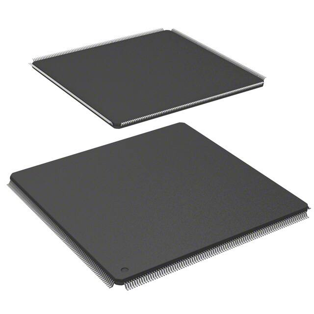


 工商网监
湘ICP备2023018690号
工商网监
湘ICP备2023018690号
