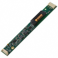
LXMG1612-05-xx
TM ®
5V Highly-Integrated, Digital Dimming CCFL Inverter Module
P RODUCTION D ATASHEET
DESCRIPTION
KEY FEATURES
W WW . Microsemi . C OM
RangeMAX Wide Range Dimming, Single Output Inverter. The LXMG1612-05-xx series of Direct Drive™ CCFL (Cold Cathode Fluorescent Lamp) Inverter Modules are specifically designed for driving LCD backlight lamps. RangeMAX Digital Dimming Technique. Digital Dimming provides flicker-free brightness control in any wide-range dimming application. The modules are equipped with a dimming input that permits brightness control from an external potentiometer, DC voltage source, or PWM signal. The resultant “burst drive” that energizes the lamp was designed specifically to ensure that no premature lamp degradation occurs.
Input Voltage Range: The modules convert DC voltage from the system battery or AC adapter directly to highfrequency, high-voltage waves required to ignite and operate CCFL lamps. A 12V input inverter is also available (LXMG1612-12-xx) Direct Drive Technology: The module design is based on a new Direct Drive topology, which provides a number of cost and performance ad-vantages. Additional Feature: Other benefits of this new topology are fixed-frequency operation and secondary-side strikevoltage regulation and all LXMG161205-xx modules feature both open and shorted lamp protection.
RangeMAX Wide Range Dimming Single 5V Input Voltage Fully Integrated Direct Drive And Dimming Control Single Sided PCB Layout Easy To Use Brightness Control MicroAmp SLEEP Mode Output Short-Circuit Protection And Automatic Strike-Voltage Regulation Fixed Frequency Operation UL 60950 E175910 RoHS Compliant APPLICATIONS
IMPORTANT: For the most current data, consult MICROSEMI’s website: http://www.microsemi.com
Protected by U.S. Patents: 5,923,129; 5,930,121; Patents Pending
Notebook And Sub-Notebook Computers Portable Instrumentation Desktop Displays Low Ambient Light Conditions (i.e. Aircraft Cabins, Automobile)
BENEFITS
PRODUCT HIGHLIGHT
DC Voltage Source
Potentiometer
PWM Signal
Microsemi
UNIVERSAL DIMMING INPUT
"PWM", V DC, OR POTENTIOMETER
1
2
BRITE
Smooth, Flicker Free 1-100% Full-Range Brightness Control Gives Your Product A High Quality Image Output Open Circuit Voltage Regulation Minimizes Corona Discharge For Long Life And High Reliability Power Efficient. “Low Brightness” Capability Allows For Advanced Power Management
3
LXMG1612-05 LXMG1612-05
PACKAGE ORDER INFO
PART NUMBER
LXMG1612-05-01 LXMG1612-05-02 LXMG1612-05-03
OUTPUT CONNECTOR
JST SM02(8.0)B-BHS-1-TB(LF)(SN) or Yeon Ho 20015WR-05A00 JST SM02B-BHSS-1-TB(LF)(SN) or Yeon Ho 35001WR-02A00 Honda QZ-19-A3MYL #02
INVERTER MATES DIRECTLY TO PANEL CONNECTORS
BHR-03VS-1 BHSR-02VS-1 Honda QZ-19-3F01
Copyright © 2000 Rev. 1.1, 2006-09-05
Microsemi
Integrated Products 11861 Western Avenue, Garden Grove, CA. 92841, 714-898-8121, Fax: 714-893-2570
Page 1
�LXMG1612-05-xx
TM ®
5V Highly-Integrated, Digital Dimming CCFL Inverter Module
P RODUCTION D ATASHEET
ABSOLUTE MAXIMUM RATINGS (NOTE 1)
W WW . Microsemi . C OM
Input Signal Voltage (VIN1) ................................................................................................................................ -0.3V to 6.5V Output Voltage, no load .........................................................................................................Internally Limited to 1800VRMS Output Current ........................................................................................................................ 8.0mARMS (Internally Limited) Output Power .................................................................................................................................................................. 6.0W Input Signal Voltage (BRITE Input) ......................................................................................................... -0.3V to VIN1+0.3V Input Signal Voltage ( SLEEP , VSYNC Inputs)............................................................................................ -0.3V to VIN1+0.3V Ambient Operating Temperature, zero airflow .....................................................................................................0°C to 70°C Storage Temperature Range .............................................................................................................................. -40°C to 85°C
Note 1: Exceeding these ratings could cause damage to the device. All voltages are with respect to Ground. Currents are positive into, negative out of specified terminal.
FUNCTIONAL PIN DESCRIPTION CONN PIN DESCRIPTION
CN1 (Molex 53261-0871) Mates with 51021-0800 housing, 50079-8100 pins
CN1-1 CN1-2 CN1-3 CN1-4 CN1-5 CN1-6 CN1-7 CN1-8
VIN1 GND SLEEP BRITE BRITE RTN VSYNC
Main Input Power Supply (4.5V < VIN1 < 5.5V Power Supply Return ON/OFF Control. (2.1V < SLEEP < VIN1 = ON, 0V < SLEEP < 0.8V = OFF, SLEEP Floating = OFF) Brightness Control (0.0V to 2.5VDC). 2.5VDC gives maximum lamp current. Analog Ground. Use for BRITE signal return ONLY. Vertical Synchronization Input. 2.5 to 5.0V Logic Level. (20Hz < fSYNC < 200Hz)
CN2 for LXMG1612-05-01 and -02 (JST SM02(8.0)B-BHS-1-TB (LF)(SN) | Yeon Ho 20015WR-05A00 or SM02B-BHSS-1-TB (LF)(SN) | Yeon Ho 35001WR-02A00)
CN2-1 CN2-2
VHI VLO
High voltage connection to high side of lamp. Connect to lamp terminal with shortest lead length. DO NOT connect to Ground. Connection to low side of lamp. Connect to lamp terminal with longer lead length. DO NOT connect to Ground High voltage connection to high side of lamp. Connect to lamp terminal with shortest lead length. DO NOT connect to Ground. Connection to low side of lamp. Connect to lamp terminal with longer lead length. DO NOT connect to Ground
PHYSICAL DIMENSIONS LXMG1612-05-XX
4.96in.
126mm
CN2 for LXMG1612-05-03 (Honda QZ-19-A3MYL#02)
CN2-3 CN2-1
VHI VLO
PACKAGE DATA PACKAGE DATA
MOUNTING HOLE 3.0mm DIA. ± .08 DIA
CN1 0.13in.
3.3mm
0.63in.
16mm
0.5in.
12.7mm
CN2
GROUNDED MOUNTING HOLE 0.66in.
16.75mm 3.0mm DIA. ± .08 DIA
3.64in.
92.5mm
0.06in.
1.52mm
0.315in.
8.0mm
Warning
High Voltage Present at all Output Connectors
PCB tolerances ± 0.5mm
Weight: 12.5 (g) typ .
Copyright © 2000 Rev. 1.1, 2006-09-05
Microsemi
Integrated Products 11861 Western Avenue, Garden Grove, CA. 92841, 714-898-8121, Fax: 714-893-2570
Page 2
�LXMG1612-05-xx
TM ®
5V Highly-Integrated, Digital Dimming CCFL Inverter Module
P RODUCTION D ATASHEET
W WW . Microsemi . C OM
RECOMMENDED OPERATING CONDITIONS (R.C.) This module has been designed to operate over a wide range of input and output conditions. However, best efficiency and performance will be obtained if the module is operated under the condition listed in the ‘R.C.’ column. Min. and Max. columns indicate values beyond which the inverter, although operational, will not function optimally. Parameter Symbol Recommended Operating Conditions Min R.C. Max Units
Input Supply Voltage Range (Fully Regulated Lamp Current) Input Supply Voltage Range (Functional) Output Power Brightness Control Input Voltage Range Lamp Operating Voltage Lamp Current (Full Brightness) Operating Ambient Temperature Range
VIN1 PO VBRT_ADJ VLAMP IOLAMP TA
4.5 4.35 0.0 450 0
5 5 3.5 2.5 535 5.8
5.5 5.65 4.0 VIN 620 70
V W V VRMS mARMS °C
ELECTRICAL CHARACTERISTICS Unless otherwise specified, the following specifications apply over the recommended operating condition and ambient temperature of 25°C except where otherwise noted. Parameter
OUTPUT PIN CHARACTERISTICS Full Bright Lamp Current Min. Average Lamp Current (Note 2) Lamp Start Voltage Operating Frequency BRITE INPUT Input Current Input Voltage for Max. Lamp Current Input Voltage for Min. Lamp Current IBRT VBRT_ADJ VBRT_ADJ V SLEEP(HI) VSLEEP(LO) I SLEEP VBRT_ADJ=0VDC VBRT_ADJ=2.5VDC IO(LAMP)=100% Duty Cycle IO(LAMP)= Minimum Duty Cycle VIN1=4.5V VIN1=5.5V -685 -260 2.30 0.0 1.9 -5.0 390 0.0 1.50 -3.0 25 20 0.0 0.5 2.1 1.9 410 0.0 2.5 0.0 27 VIN1 2.0 435 0.0 5.0 1.2 29 200 10 -728 -282 2.35 -775 -305 2.40 µADC µADC VDC VDC VDC VDC µADC µADC VDC VDC KΩ Hz µADC IL(MAX) IL(MIN) VLS fO VBRT_ADJ=2.5VDC, SLEEP=HIGH, Burst Duty=100%, VIN1=5VDC VBRT_ADJ=0VDC, SLEEP=HIGH, Burst Duty=2.0%, VIN1=5VDC 0°C 5.0VDC VBRT_ADJ=2.5VDC, SLEEP=HIGH, VIN1=5.0V 5.2 5.8 0.12 1500 63 1650 68 1800 73 6.4 mARMS mARMS VRMS kHz
Symbol
Test Conditions
LXMG1612-05-xx Min Typ Max
Units
SLEEP INPUT
RUN Mode
SLEEP Mode
Input Current VSYNC CHARACTERISTICS Logic High Level Input Impedance Input Frequency POWER CHARACTERISTICS
SLEEP=5.0V SLEEP=0V
VIN1=4.5V VIN1=5.5V
ELECTRICALS
VSYNCH(HI) VSYNCH(LO) ZIN fSYNC
VIN1=5VDC, SLEEP=0.0V Sleep Current IIN(MIN) Note 2: Minimum lamp current required to maintain even light output may vary with display panel. Average RMS current = (Burst Duty Cycle) x (Burst amplitude of 5.8mARMS) Copyright © 2000 Rev. 1.1, 2006-09-05
Microsemi
Integrated Products 11861 Western Avenue, Garden Grove, CA. 92841, 714-898-8121, Fax: 714-893-2570
Page 3
�LXMG1612-05-xx
TM ®
5V Highly-Integrated, Digital Dimming CCFL Inverter Module
P RODUCTION D ATASHEET
HOW RANGEMAX WORKS
W WW . Microsemi . C OM
LAMP VOLTAGE & LAMP CURRENT – Burst Mode Operation
Figure 1 – 50% Burst Duty Cycle
Figure 2 – 2% Burst Duty Cycle
Rather than using the traditional dimming technique of varying lamp current magnitude to adjust light output, RangeMAX inverters use a fixed lamp current value with a duty cycle control method. The lamp current burst width can be modulated from 100% (continuous lamp current) down to a 2% duty cycle, allowing the lamp to be dimmed to less than 1% of its full brightness. As can be seen in Trace 4 of Figure 3 photo at right, careful design consideration was given to controlling lamp start voltage to softly start current flow. This eliminates current overshoot that can result in premature cathode wear and reduce lamp life.
Figure 3 – 2% Burst Duty Cycle (Expanded Time Base)
High Voltage Transformer Transformer Driver
LAMP
Comparator V BRITE + 0.25 2.5V DC Ramp
V HI
Ramp Gen
V SENSE ISENSE
V LO
DESCRIPTION DESCRIPTION
V SYNC
Figure 4 – RangeMAX Block Diagram
Copyright © 2000 Rev. 1.1, 2006-09-05
Microsemi
Integrated Products 11861 Western Avenue, Garden Grove, CA. 92841, 714-898-8121, Fax: 714-893-2570
Page 4
�LXMG1612-05-xx
TM ®
5V Highly-Integrated, Digital Dimming CCFL Inverter Module
P RODUCTION D ATASHEET
HOW RANGEMAX WORKS (CONTINUED)
W WW . Microsemi . C OM
Highlights
Integrated brightness control circuit includes a DC voltage to pulse width converter that minimizes system design work and system noise susceptibility. This provides a familiar and convenient interface while reducing the potential for externally induced noise, which can cause lamp flicker. RangeMAX inverter modules are designed to operate with the burst frequency synchronized to the video frame rate. This provides operation with no visible display disturbances caused by beat frequencies between the lamps and video frame rates. In this synchronous mode, the inverter burst rate operates at twice the video refresh rate, well beyond standard 50/60Hz video refresh rates where the eye can perceive pulsing light. In applications with no access to a vertical sync., an onboard oscillator operates the inverter burst rate at about 250Hz. In this non-synchronous mode, minor display disturbances can be found under certain video conditions. This performance may be acceptable for many applications, but synchronization must be used when no disturbance can be tolerated. A single input will accommodate negative and positive vertical sync pulses at any pulse width. Separate feedback loops for lamp current and open circuit voltage regulation insure reliable strike under all operating conditions, automatic over-voltage prevention with broken or failed lamps, and accurate lamp current regulation.
TYPICAL APPLICATION
5V DAC or Pot 10k LXMG1612-05-xx R BRITE RTN SLEEP VSYNC GND VLO CCFL TUBE
BRITE
VIN1
VHI
The brightness control may be a voltage output DAC, digital resistor or a simple 10k potentiometer. If desired, an additional series resistor with the 10k potentiometer can be used to set a higher minimum brightness setting as shown in Figure 5. A 2.5V to 5V Logic Level PWM signal from a micro-controller may also be used as shown in Figure 5A. If synchronization to the video frame rate is desired, connect the vertical sync pulse from the system video controller to the VSYNC input. If no video synchronization is desired, connect VSYNC to ground. If you need to turn the inverter ON/OFF remotely, connect to 2.5V to 5V logic signal to the SLEEP input. Connect VHI to high voltage wire from the lamp. Connect VLO to the low voltage wire (wire with thinner insulation). Never connect VLO to circuit ground as this will defeat lamp current regulation. If both lamp wires have heavy high voltage insulation, connect the longest wire to VLO. This wire is typically white.
5V 0V VSYNC
Figure 5 - Potentiometer Brightness Control
PWM Signal from System P.W.
BRITE
LXMG1612-05-xx
2ms 0 < P.W. < 100% of period Figure 5A - PWM Brightness Control
LXMG1612-05-XX OUTPUT CURRENT ADJUST
D DESCRIPTION
The LXMG1612-05 output current can be adjusted by changing the value of two resistors on the PCB. The following table shows the approximate new output current values:
Output Current 7.0mA 6.0mA 5.8mA 5.0mA 4.0mA 3.0mA Copyright © 2000 Rev. 1.1, 2006-09-05 R12 2.00K 1% 2.61K 1% 2.74K 1% 2.74K 1% 2.74K 1% 2.74K 1% R16 Not Used Not Used Not Used 499K 1% 178K 1% 78.7K 1%
R30 U4
R33
R34 R4 C3 C4 R2 C5 R3 C2 C9
D2
R7 C11 C15 C12 R11 R12
R15 R14 C16
U3
R21 C7 R20 R41 R40
D1
C21
R31
R32
R38 R35 R36 R37 R39 R17
R5 R6
C13 R16 R10
C10
R13
Figure 6- Component Replacement Locations
Microsemi
Integrated Products 11861 Western Avenue, Garden Grove, CA. 92841, 714-898-8121, Fax: 714-893-2570
C17
C6
C8
U1
C14
Page 5
�LXMG1612-05-xx
TM ®
5V Highly-Integrated, Digital Dimming CCFL Inverter Module
P RODUCTION D ATASHEET
NOTES
W WW . Microsemi . C OM
NOTES NOTES
PRODUCTION DATA – Information contained in this document is proprietary to Microsemi and is current as of publication date. This document may not be modified in any way without the express written consent of Microsemi. Product processing does not necessarily include testing of all parameters. Microsemi reserves the right to change the configuration and performance of the product and to discontinue product at any time.
Copyright © 2000 Rev. 1.1, 2006-09-05
Microsemi
Integrated Products 11861 Western Avenue, Garden Grove, CA. 92841, 714-898-8121, Fax: 714-893-2570
Page 6
�


 工商网监
湘ICP备2023018690号
工商网监
湘ICP备2023018690号
