Ultra Low Noise, Medium Current
E-PHEMT Transistor
50Ω
TAV2-14LN+
0.05 to 10 GHz
The Big Deal
• Low Noise Figure, 0.6 dB typ. at 6 GHz, 2V
• High Gain, 16.4 dB typ. at 6 GHz, 4V
• High OIP3, +30.9 dBm typ. at 6 GHz, 4V
• High P1dB, 18.8 dBm typ. at 6 GHz, 4V
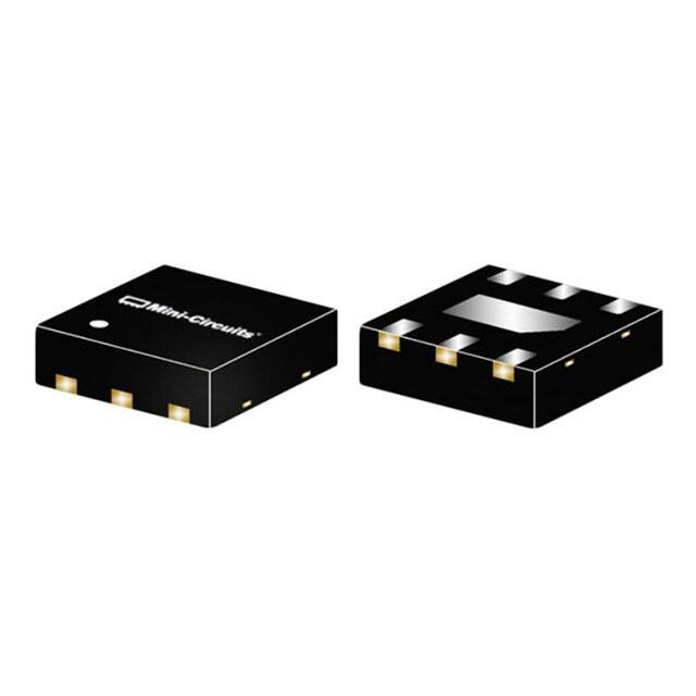
2mm x 2mm
Product Overview
Mini-Circuits’ TAV2-14LN+ is a MMIC E-PHEMT* transistor with an operating frequency range from 0.05 to
10 GHz. This model combines high gain with extremely low noise figure, resulting in lower overall system
noise. Low NF and IP3 performance make it an ideal choice for sensitive receivers in communications systems. Manufactured using highly repeatable E-PHEMT technology, the unit comes housed in a tiny 2x2mm
MCLP package. This model requires external biasing and matching.
Key Features
Feature
Advantages
Wideband, 0.05 to 10 GHz
Usable to 12 GHz
A single device covers many wireless communications bands including cellular, ISM,
GSM, WCDMA, WiMax, WLAN, 5G and more.
High IP3 vs. DC power consumption
• +30.9 dBm at 6 GHz, 4V
• +33.2 dBm at 12 GHz, 4V
The TAV2-14LN+ matches industry leading IP3 performance relative to device size
and power consumption. Enhanced linearity over a broad frequency range makes the
device ideal for use in:
• Driver amplifiers for complex waveform up converter paths
• Drivers in linearized transmit systems
Combines high gain (16.4 dB) with very
low Noise Figure (0.7 dB)
The unique combination of high gain and low Noise Figure results in lower overall
system noise.
2 x 2mm 6-lead MCLP package
Tiny footprint saves space in dense layouts while providing low inductance, repeatable
transitions, and excellent thermal contact to the PCB.
* Enhancement mode Pseudomorphic High Electron Mobility Transistor.
Notes
A. Performance and quality attributes and conditions not expressly stated in this specification document are intended to be excluded and do not form a part of this specification document.
B. Electrical specifications and performance data contained in this specification document are based on Mini-Circuit’s applicable established test performance criteria and measurement instructions.
C. The parts covered by this specification document are subject to Mini-Circuits standard limited warranty and terms and conditions (collectively, “Standard Terms”); Purchasers of this part are entitled
to the rights and benefits contained therein. For a full statement of the Standard Terms and the exclusive rights and remedies thereunder, please visit Mini-Circuits’ website at www.minicircuits.com/MCLStore/terms.jsp
Mini-Circuits
®
www.minicircuits.com P.O. Box 350166, Brooklyn, NY 11235-0003 (718) 934-4500 sales@minicircuits.com
Page 1 of 5
�Ultra Low Noise, Medium Current
E-PHEMT Transistor
50Ω
TAV2-14LN+
0.05 to 10 GHz
Product Features
• Low Noise Figure, 0.6 dB typ. at 6 GHz, 2V,
• Gain, 16.4 dB typ. at 6 GHz, 4V
• High Output IP3, +30.9 dBm at 6 GHz, 4V
• Output Power at 1dB comp., +18.8 dBm at 6 GHz, 4V
• External biasing and matching required
• Usable to 12 GHz
Generic photo used for illustration purposes only
CASE STYLE: MC1630-1
Typical Applications
+RoHS Compliant
The +Suffix identifies RoHS Compliance. See our web site
for RoHS Compliance methodologies and qualifications
• 5G
• Cellular
• ISM
• GSM
• WCDMA
• WiMax
• WLAN
• UNII and HIPERLAN
General Description
Mini-Circuits’ TAV2-14LN+ is a MMIC E-PHEMT* transistor with an operating frequency range from 0.05 to
10 GHz. This model combines high gain with extremely low noise figure, resulting in lower overall system
noise. Low NF and IP3 performance make it an ideal choice for sensitive receivers in communications systems. Manufactured using highly repeatable E-PHEMT technology, the unit comes housed in a tiny 2x2mm
MCLP package. This model requires external biasing and matching.
simplified schematic and pin description
DRAIN
GATE
SOURCE
Function
Pin Number
Description
RF-IN
2
Gate used for RF input
RF-OUT
5
Drain used for RF output
GND
1,3,4,6 & Paddle
Source terminal, normally connected to ground.
Notes
A. Performance and quality attributes and conditions not expressly stated in this specification document are intended to be excluded and do not form a part of this specification document.
B. Electrical specifications and performance data contained in this specification document are based on Mini-Circuit’s applicable established test performance criteria and measurement instructions.
C. The parts covered by this specification document are subject to Mini-Circuits standard limited warranty and terms and conditions (collectively, “Standard Terms”); Purchasers of this part are entitled
to the rights and benefits contained therein. For a full statement of the Standard Terms and the exclusive rights and remedies thereunder, please visit Mini-Circuits’ website at www.minicircuits.com/MCLStore/terms.jsp
Mini-Circuits
®
www.minicircuits.com P.O. Box 350166, Brooklyn, NY 11235-0003 (718) 934-4500 sales@minicircuits.com
REV. OR
ECO-001966
TAV2-14LN+
GY/RS/CP
200227
Page 2 of 5
�TAV2-14LN+
E-PHEMT Transistor
Electrical Specifications at TAMB=25°C
Symbol
Parameter
Condition
Min.
Typ.
Max.
Units
DC Specifications
VTH
Threshold Voltage
VDS=4V, IDS=4 mA
IDSS
Saturated Drain Current
VDS=4V, VGS=0 V
—
0.37
2.0
—
µA
V
GM
Transconductance
VDS =4V, Gm =∆IDS/∆VGS,
∆VGS = VGS2-VGS1,
VGS2=0.7V, VGS1=0.6V
∆IDS =(IDS at VGS2)-(IDS at VGS1)
—
192
—
mS
IGSS
Gate leakage Current
VGD=VGS=-3V
—
1.0
µA
RF & DC Specifications, Z0=50 Ohms
Parameter
Gain
Input Return Loss
Output Return Loss
P1dB3
OIP3
Pout=5dBm/Tone
Noise Figure
VDS = 4V1,
IDS = 40mA
Condition (GHz)
VDS = 2V1
IDS = 20mA
VS = 5V2
VS = 3V2
Typ.
Typ.
Typ.
Min.
Typ.
Max.
0.05
21
23.4
25.7
22
—
—
6
14.7
16.4
18
15.9
12.7
11.9
8
12.5
13.9
15.3
13.3
10.1
9.4
10
10.8
11.8
13.2
11.3
9.8
9.1
12
—
10.2
—
10
—
—
0.05
—
—
—
—
—
—
6
7
6
11
10
8
7
6
15
12
10
7
7
8
7
12
8
7
—
—
0.05
5
5
—
—
6
13
13
7
7
8
20
17
8
9
10
20
17
7
7
—
12
19
16
—
0.05
17.7
13.3
—
—
6
18.8
13.1
12.6
8.5
8
19.1
13.4
11.2
7.4
10
19.4
13.5
13.4
10.2
—
12
19.1
13
—
0.05
27.1
22.8
—
—
6
30.9
24.9
25.9
20.8
8
31.6
25.9
25.4
18.6
10
33.0
28.5
27.0
21.8
—
12
33.2
29.0
—
0.05
2.5
0.7
—
—
6
0.7
0.6
0.8
0.7
8
0.7
0.6
1.0
0.8
10
0.8
0.7
1.0
0.7
Units
dB
dB
dB
dBm
dBm
dB
12
1.0
0.8
—
—
IDS
DC
40
20
54
23
mA
VGS
DC
0.58
—
—
V
0.44
0.65
0.72
1. Measured in test board TB-TAV2-14LN+. See Fig 1.
2. Measured in eval board TB-TAV2-14LNE+ (designed for 6-10 GHz). See Fig. 2.
3. Drain current bias allowed to increase during compression measurement.
Notes
A. Performance and quality attributes and conditions not expressly stated in this specification document are intended to be excluded and do not form a part of this specification document.
B. Electrical specifications and performance data contained in this specification document are based on Mini-Circuit’s applicable established test performance criteria and measurement instructions.
C. The parts covered by this specification document are subject to Mini-Circuits standard limited warranty and terms and conditions (collectively, “Standard Terms”); Purchasers of this part are entitled
to the rights and benefits contained therein. For a full statement of the Standard Terms and the exclusive rights and remedies thereunder, please visit Mini-Circuits’ website at www.minicircuits.com/MCLStore/terms.jsp
Mini-Circuits
®
www.minicircuits.com P.O. Box 350166, Brooklyn, NY 11235-0003 (718) 934-4500 sales@minicircuits.com
Page 3 of 5
�TAV2-14LN+
E-PHEMT Transistor
Absolute Maximum Ratings4
Symbol
Parameter
Max.
Units
IGS
PDISS
Drain-Source Voltage
Gate-Source Voltage at VDS=4V
Drain Current at VDS=4V
Gate Current
Total Dissipated Power
5
-5 &1
65
15
325
V
V
mA
µA
mW
PIN6
RF Input Power
18 (5-minute max.)
15 (continuous)
dBm
TCH
Channel Temperature
150
°C
TOP
Operating Temperature
-40 to 85
°C
TSTD
Storage Temperature
-65 to 150
°C
θjc
Thermal Resistance
170
°C/W
VDS5
VGS5
IDS5
4. Operation of this device above any one of these parameters may cause permanent damage.
5. Assumes DC quiescent conditions.
6. IGS is limited to 15µA during test.
Characterization Test Circuit
Fig 1. Block Diagram of Test Circuit used for characterization. (DUT is soldered on Mini-Circuits Test Board TB-TAV2-14LN+)
Gain, Output power at 1dB compression (P1dB), Noise Figure and output IP3 (OIP3) are measured using Agilent’s Microwave Network
Analyzer N5242A PNA-X.
Conditions:
1. Drain voltage (with reference to source, VDS)= 2V&4V as shown.
2. Gate Voltage (with reference to source, VGS) is set to obtain desired Drain-Source current (IDS) as shown in graphs or specification table.
3. Gain: Pin= -25dBm
4. Output IP3 (OIP3): Two tones, spaced 1 MHz apart, 5 dBm/tone at output.
5. No external matching components used.
Application Test Circuit
Fig 2. Block Diagram of Test Circuit used for characterization. (DUT is soldered on Mini-Circuits Application test board TB-TAV2-14LNE+)
Gain, Return loss, Output power at1dB compression (P1dB), output IP3 (OIP3) and noise figure measured using Agilent’s
microwave network analyzer N5242A PNA-X.
Conditions:
1. Supply voltage, VS=3V&5V
Notes
2. Gain
and Return
Pin= -25dBm
A. Performance
and quality
attributesloss:
and conditions
not expressly stated in this specification document are intended to be excluded and do not form a part of this specification document.
B. Electrical3.specifications
performance
contained
in this
specification
are based
on Mini-Circuit’s applicable established test performance criteria and measurement instructions.
Output IP3and
(OIP3):
Two data
Tones
spaced
1 MHz
apart,document
5dBm/ tone
at output.
C. The parts covered by this specification document are subject to Mini-Circuits standard limited warranty and terms and conditions (collectively, “Standard Terms”); Purchasers of this part are entitled
to the rights and benefits contained therein. For a full statement of the Standard Terms and the exclusive rights and remedies thereunder, please visit Mini-Circuits’ website at www.minicircuits.com/MCLStore/terms.jsp
Mini-Circuits
®
www.minicircuits.com P.O. Box 350166, Brooklyn, NY 11235-0003 (718) 934-4500 sales@minicircuits.com
Page 4 of 5
�TAV2-14LN+
E-PHEMT Transistor
Product Marking
MCL
T214
Marking may contain other features or characters for internal lot control
Additional Detailed Technical Information
additional information is available on our dash board. To access this information click here
Data Table
Performance Data
Swept Graphs
S-Parameter (S2P Files) Data Set (.zip file)
Case Style
MC1630-1 Plastic package, exposed paddle, lead finish: Matte-Tin
Tape & Reel
F55
Standard quantities available on reel
7” reels with 20, 50, 100, 200, 500 or 1K devices
Suggested Layout for PCB Design
PL-659
Evaluation Board
TB-TAV2-14LN+ & TB-TAV2-14LNE+
Environmental Ratings
ENV08T1
ESD Rating
Human Body Model (HBM): Class 0 (50V to 250V) in accordance with ANSI/ESD STM 5.1 - 2001
MSL Test Flow Chart
Start
Visual
Inspection
Electrical Test
SAM Analysis
Reflow 3 cycles,
260°C
Soak
85°C/85RH
168 hours
Bake at 125°C,
24 hours
Visual
Inspection
Electrical Test
SAM Analysis
Finish
Additional Notes
A. Performance and quality attributes and conditions not expressly stated in this specification document are intended
to be excluded and do not form a part of this specification document.
B. Electrical specifications and performance data contained in this specification document are based on Mini-Circuit’s
applicable established test performance criteria and measurement instructions.
C. The parts covered by this specification document are subject to Mini-Circuits standard limited warranty and terms
and conditions (collectively, “Standard Terms”); Purchasers of this part are entitled to the rights and benefits
Notes
contained therein. For a full statement of the Standard Terms and the exclusive rights and remedies thereunder,
A. Performance and quality attributes and conditions not expressly stated in this specification document are intended to be excluded and do not form a part of this specification document.
please visit
B. Electrical specifications
and Mini-Circuits’
performance datawebsite
containedatinwww.minicircuits.com/MCLStore/terms.jsp
this specification document are based on Mini-Circuit’s applicable established test performance criteria and measurement instructions.
C. The parts covered by this specification document are subject to Mini-Circuits standard limited warranty and terms and conditions (collectively, “Standard Terms”); Purchasers of this part are entitled
to the rights and benefits contained therein. For a full statement of the Standard Terms and the exclusive rights and remedies thereunder, please visit Mini-Circuits’ website at www.minicircuits.com/MCLStore/terms.jsp
Mini-Circuits
®
www.minicircuits.com P.O. Box 350166, Brooklyn, NY 11235-0003 (718) 934-4500 sales@minicircuits.com
Page 5 of 5
�


 工商网监
湘ICP备2023018690号
工商网监
湘ICP备2023018690号
