Freescale Semiconductor Technical Data
MPXY8000 Rev 1, 12/2004
Tire Pressure Monitoring Sensor Temperature Compensated and Calibrated, Fully Integrated, Digital Output
The Freescale Semiconductor MPXY8000 series sensor is an 8-pin tire monitoring sensor which is comprised of a variable capacitance pressure sensing element, a temperature sensing element, and an interface circuit (with a wake-up feature) all on a single chip. It is housed in a Super-Small Outline Package (SSOP), which includes a media protection filter. Specifically designed for the low power consumption requirements of tire pressure monitoring systems, it can combine with a Freescale Semiconductor remote keyless entry (RKE) system to facilitate a low-cost, highly integrated system. Detailed Description The block diagram of the MPXY8000 series sensor is shown in Figure 1. The pressure sensor is a capacitive transducer constructed using surface micromachining, the temperature sensor is constructed using a diffused resistor, and the interface circuit is integrated onto the same die as the sensors using a standard silicon CMOS process. The conditioning of the pressure signal begins with a capacitance to voltage conversion (C to V) followed by a switched capacitor amplifier. This amplifier has adjustable offset and gain trimming. The offset and gain are factory calibrated, with calibration values stored in the EEPROM trim register. This amplifier also has temperature compensation circuits for both sensitivity and offset, which also are factory adjusted using the EEPROM trim register. The pressure is monitored by a voltage comparator, which compares the measured value against an 8-bit threshold adjusted by a serial input. By adjusting the threshold and monitoring the state of the OUT pin the external device can check whether a low-pressure threshold has been crossed, or perform up to 8-bit A/D conversions. The temperature is measured by a diffused resistor with a positive temperature coefficient driven by a current source, thereby creating a voltage. The room temperature value of this voltage is factory calibrated using the EEPROM trim register. A two-channel multiplexer can route either the pressure or temperature signal to a sampling capacitor that is monitored by a voltage comparator with variable threshold adjust, providing a digital output for temperature. An internal low frequency, low power 5.4 kHz oscillator with a 14-stage divider provides a periodic pulse to the OUT pin (divide by 16384 for 3 seconds). This pulse can be used to wake up an external MCU to begin an interface with the device. An additional 10-stage divider will provide a pulse every 52 minutes which can be used to reset an external MCU. The power consumption can be controlled by several operational modes selected by external pins.
MPXY8020A MPXY8040A
TIRE PRESSURE MONITORING SENSOR MPXY8020A: OPTIMIZED FOR 250 kPa – 450 kPa MPXY8040A: OPTIMIZED FOR 500 kPa – 900 kPa
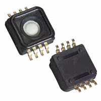
SUPER SMALL OUTLINE PACKAGE CASE 1352-03
PIN ASSIGNMENT
S1/VPP 1 VDD 2 VSS 3 OUT 4
8 SO 7 CLK 6 DATA 5 RST
8-pin Super Small Outline Package (SSOP)
ORDERING INFORMATION
Shipped In Rails MPXY8020A6U MPXY8040A6U Shipped in Tape & Reel MPXY8020A6T1 MPXY8040A6T1
© Freescale Semiconductor, Inc., 2004. All rights reserved.
�VDD PX Clock Gen fHF Internal HF OSC. Power Control PREF C to V Convert Digital Control S1 S0 Data CLK
AMP Internal LF OSC.
P-Cell
P-Off Trim
P-Gain Trim
P-TCO Trim
P-TCS Trim
f LF 14-Stage Divider Lock 10-Stage Divider
T-Off Trim
8-Bit Current Source 2-Chan MUX
8-Bit D/A Register
RST
2-Chan MUX t PTC Res. AVSS
COMP + Sample CAP AVSS
3-Chan MUX
OUT VSS
AVSS
Figure 1. MPXY8000 Series Sensor Block Diagram Operating Modes The device has several operating modes dependent on the applied voltages to the S1 and S0 pins as shown in Table 1. In all the modes listed the channel multiplexers, D/A Register, LFO, and the output pulse dividers will always be powered up as long as there is a voltage source connected to the VDD pin. When only the S0 pin is at a logic one the pressure measuring circuit in the device is powered up and the pressure output signal is connected to the sample capacitor through a multiplexer. When the S0 pin returns to the low state the multiplexer will first turn off to store the signal on the sample capacitor before powering down the measuring circuitry. When only the S1 pin is at a logic one the temperature measuring circuit in the device is powered up and the temperature output signal is connected to the sample capacitor through a multiplexer. When the S1 pin returns to the low state the multiplexer will first turn off to store the signal on the sample capacitor before powering down the measuring circuitry. NOTE: All of the EEPROM trim bits will be powered up regardless of whether the pressure or temperature measuring circuitry is activated. NOTE: If the voltage on the S1 pin exceeds 2.5 times the voltage on the VDD pin the device will be placed into its Trim/ Test Mode. NOTE: If the VDD supply source is switched off in order to reduce current consumption, it is important that all input pins be driven LOW to avoid powering up the device. If any input pin (S1, S0, DATA, or CLK) is driven HIGH while the VDD supply is switched off, the device may be powered up through an ESD protection diode. In such a case, the effective VDD voltage will be about 0.3 V less than the voltage applied to the input pin, and the full device IDD current will be drawn from the device driving input.
MPXY8000 2 Sensor Devices Freescale Semiconductor
�Table 1. Operating Modes
Circuitry Powered S1 S0 Operating Mode Pressure Measure System OFF ON OFF OFF Temp Measure System OFF OFF ON OFF A/D Output Comp. OFF OFF OFF ON LFO Oscill. ON ON ON ON Serial Data Counter
0 0 1 1
0 1 0 1
Standby/Reset Measure Pressure Measure Temperature Output Read
ACTIVE RESET RESET ACTIVE
Pin Functions The following paragraphs give a description of the general function of each pin. VDD and VSS Pins Power is supplied to the control IC through VDD and VSS. VDD is the positive supply and VSS is the digital and analog
ground. The control IC operates from a single power supply. Therefore, the conductors to the power supply should be connected to the VDD and VSS pins and locally decoupled as shown in Figure 2.
MPXY8020A VDD
To Other VDD Loads VDD 0.1 µF VSS To Other VSS Returns VSS To Power Supply
Figure 2. Recommended Power Supply Connections OUT Pin The OUT pin normally provides a digital signal related to the voltage applied to the voltage comparator and the threshold level shifted into an 8-bit register from an external device. When the device is placed in the standby mode the OUT pin is driven high and will be clocked low when an overflow is detected from a clock divider (divide by 16384) driven by the LFO. This allows the OUT pin to wake up an external device such as an MCU.
OUT
2/f LFO
2/f LFO
Operation
Measure
Standby
Measure 3 Sec
Wake Up
Figure 3. Pulse on OUT Pin During Standby Mode RST Pin The RST pin is normally driven high and will be clocked low when an overflow is detected from total clock divider (divide by 16,777,216) driven by the LFO. This allows the RST pin to reset an external device such as an MCU. This pulse will appear on the RST pin approximately every
52 minutes regardless of the operating mode of the device. The pulse lasts for two cycles of the LFO oscillator as shown in Figure 4. Since the RST pin is clocked from the same divider string as the OUT pin, there will also be a pulse on the OUT pin when the RST pin pulses every 52 minutes.
MPXY8000 Sensor Devices Freescale Semiconductor 3
�OUT RST
2/f LFO 2/f LFO
Standby
≈ 3 Sec ≈ 52 Minutes
Figure 4. Pulse on RST Pin S0 Pin The S0 pin is used to select the mode of operation as shown in Table 1. The S0 pin contains an internal Schmitt trigger as part of its input to improve noise immunity. The S0 pin has an internal pull-down device in order to provide a low level when the pin is left unconnected. S1 Pin The S1 pin is used to select the mode of operation, as shown in Table 1. The S1 pin contains an internal Schmitt trigger as part of its input to improve noise immunity. This pin has an internal pull-down device to provide a low level when the pin is left unconnected. The S1 pin also serves the purpose of enabling factory trim and test of the device. The higher VPP programming voltage for the internal EEPROM trim register is also supplied through the S1 pin. DATA Pin The DATA pin is the serial data in (SDI) function for setting the threshold of the voltage comparator. The DATA pin contains an internal Schmitt trigger as part of its input to improve noise immunity. This pin has an internal pull-down device to provide a low level when the pin is left unconnected. Table 2. D/A Threshold Bit Assignment
Function LSB Bit Weight 1 2 4 Voltage Comparator Threshold Adjust (8 bits) 8 16 32 64 MSB 128 Data Bit D0 D1 D2 D3 D4 D5 D6 D7
CLK Pin The CLK pin is used to provide a clock used for loading and shifting data into the DATA pin. The data on the DATA pin is clocked into a shift register on the rising edge of the CLK pin signal. The data is transferred to the D/A Register on the eighth falling edge of the CLK pin. This protocol may be handled by the SPI or SIOP serial I/O function found on some MCU devices. The CLK pin contains an internal Schmitt trigger as part of its input to improve noise immunity. The CLK pin has an internal pull-down device to provide a low level when the pin is left unconnected. Output Threshold Adjust The state of the OUT pin is driven by a voltage comparator whose output state depends on the level of the input voltage on the sample capacitor and the level of an adjustable 8-bit threshold voltage. The threshold is adjusted by shifting data bits into the D/A Register (DAR) via the DATA pin while clocking the CLK pin. The timing of this data is shown in Figure 4. Data is transferred into the serial shift register on the rising edge of the CLK pin. On the falling edge of the 8th clock the data in the serial shift register is latched into the parallel DAR register. The DAR remains powered up whenever VDD is present. The serial data is clocked into the DATA pin starting with the MSB first. This sequence of threshold select bits is shown in Table 2.
MPXY8000 4 Sensor Devices Freescale Semiconductor
�An analog to digital (A/D) conversion can be accomplished with eight (8) different threshold levels in a successive approximation algorithm; or the OUT pin can be set to trip at some alarm level. The voltage on the sample capacitor will maintain long enough for a single 8-bit conversion, but may need to be refreshed with a new measured reading if the read interval is longer than the specified hold time, tSH. The counter that determines the number of clock pulses into the device is reset whenever the device is placed into the Measure Pressure or Measure Temperature Modes. This provides a means to reset the data transfer count in case the
1 CLK Data MSB BIT6 BIT5 BIT4 2 3 4
clock stream is corrupted during a transmission. In these two modes the DATA and CLK pins should not be clocked to reduce noise in the captured pressure or temperature data. Any change in the DAR contents should be done during the Standby or Output Read Modes. Both the serial bit counter and the state of the DAR are undefined following power up of the device. The serial bit counter can be reset by cycling either the SO pin or the S1/VPP pin to a high level and then back low. The DAR can then be reset to the lowest level by holding the DATA pin low while bursting the CLK pin with eight (8) clock pulses.
5 6 7 8
BIT3
BIT2
BIT1
LSB
Serial Data ∗
MSB
BIT6
BIT5
BIT4
BIT3
BIT2
BIT1
LSB
DAR Load *
DAR * (*) Denotes Internal Signal
Data
Figure 5. Serial Data Timing Pressure Sensor Output The pressure channel compares the output of its analog measurement circuit to the D/A reference voltage. The device is calibrated at two different nominal values depending on the calibration option. APPLICATIONS Suggested application example is shown in Figure 6. Temperature Sensor Output The temperature channel compares the output of a positive temperature coefficient (PTC) resistor driven by a switched current source. The current source is only active when the temperature channel is selected.
Optional
+
Motion Sense
VDD
S1 S0 Data State Machine or MCU RF Transmitter
3.0 V MPXY8000 Series Sensor
0.1 µF
CLK RST OUT
VSS
Figure 6. Application Example
MPXY8000 Sensor Devices Freescale Semiconductor 5
�ELECTRICAL SPECIFICATIONS Maximum ratings are the extreme limits to which the device can be exposed without permanently damaging it. The device contains circuitry to protect the inputs against damage Table 3. Maximum Ratings Rating
Supply Voltage Short Circuit Capability (all pins excluding VDD and VSS) Maximum High Voltage for 5 minutes Minimum Low Voltage for 5 minutes Substrate Current Injection Current from any pin to VSS –0.3 VDC) Electrostatic Discharge Human Body Model (HBM) Charged Device Model (CDM) Machine Model (MM) Storage Temperature Range Standard Temperature Range
from high static voltages; however, do not apply voltages higher than those shown in the table below. Keep VIN and VOUT within the range VSS ≤ (VIN or VOUT) ≤ VDD.
Symbol
VDD VSC VSC
Value –0.3 to +4.0
VDD VSS
Unit
V V V
ISUB
600 ±1000 ±1000 ±200
µA
VESD VESD VESD Tstg
V V V
–40 to +150
°C
ELECTRO STATIC DISCHARGE (ESD) WARNING: This device is sensitive to electrostatic discharge. Extra precaution must be taken by the user to protect the chip from ESD. A charge of over 1000 volts can accumulate on the human body or associated test equipment. A charge
of this magnitude can alter the performance or cause failure of the chip. When handling the pressure sensor, proper ESD precautions should be followed to avoid exposing the device to discharges which may be detrimental to its performance.
Operating Range The limits normally expected in the application which define range of operation. Table 4. Operating Range Characteristic
Supply Voltage Operating Temperature Range Standard Temperature Range Supply Current Drain Standby Mode −40°C to +85°C +85°C to +100°C +100°C to +125°C Read Mode −40°C to +125°C Measure Temperature Mode −40°C to +125°C Measure Pressure Mode −40°C to +10°C +10°C to +60°C +60°C to +125°C
Symbol
VDD
Min
2.1
Typ
3.0
Max
3.6
Units
V
TL TA
–40
—
TH +125
°C
ISTBY ISTBY ISTBY
— — —
0.6 0.8 1.5
0.9 1.2 2.2
µA µA µA
IREAD
—
400
600
µA
ITEMP
—
400
600
µA
IPRESS IPRESS IPRESS
— — —
1400 1300 1200
1800 1700 1700
µA µA µA
MPXY8000 6 Sensor Devices Freescale Semiconductor
�Table 5. Electrical Characteristics +2.1 V ≤ VDD ≤ +3.6 V, TL ≤ TA ≤ TH, unless otherwise specified. Characteristic
Output High Voltage DATA, OUT, RST (ILoad = 100 µA) Output Low Voltage DATA, OUT, RST (ILoad = -100 µA) Input High Voltage S0, S1, DATA, CLK Input Low Voltage S0, S1, DATA, CLK Input Hysteresis (VIH — VIL) S0, S1, DATA, CLK Input Low Current (at VIL) S0, S1, DATA, CLK Input High Current (at VIH) S0, S1, DATA, CLK Temperature Measurement (+2.5 V ≤ VDD ≤ 3.0 V) D/A Conversion Code at –40°C D/A Conversion Code at –20°C D/A Conversion Code at 25°C D/A Conversion Code at 70°C D/A Conversion Code at 100°C D/A Conversion Code at 120°C D/A Conversion Code at 125°C Temperature Measurement (+2.1 V ≤ VDD ≤ 3.6 V) D/A Conversion Code at –40°C D/A Conversion Code at –20°C D/A Conversion Code at 25°C D/A Conversion Code at 70°C D/A Conversion Code at 100°C D/A Conversion Code at 120°C D/A Conversion Code at 125°C Temperature Sensitivity at 25°C Approximate Temperature Output Response T–40 T–20 T25 T70 T100 T120 T125 36 52 97 154 203 240 249 — 42 57 102 163 214 252 255 0.80 49 64 107 172 225 255 255 counts counts counts counts counts counts counts °C/bit counts T–40 T–20 T25 T70 T100 T120 T125 36 52 97 155 204 241 249 42 57 102 163 214 252 255 47 62 107 171 224 255 255 counts counts counts counts counts counts counts
Symbol
VOH VOL VIH VIL VHYS IIL IIH
Min
VDD –0.8 —
Typ
—
Max
—
Units
V
—
0.4
V
0.7 x VDD VSS 100
— — 200
— 0.3 x VDD —
V V mV µA
–5 –5
–25 –35
–100 –140
µA (2)
OUT = 74.7461 + 0.9752 x Ta + 0.0041 x Ta^2
8 7 6
Temperature Error (°C)
5 4 3 2 1 0 -40 -20 0 20 40 60 80 100 120
Temperature (°C)
Figure 7. Temperature Error vs Temperature at VDD = 3.0 V MPXY8000 Sensor Devices Freescale Semiconductor 7
�Table 6. Control Timing +2.1 V ≤ VDD ≤ +3.6 V, TL ≤ TA ≤ TH, unless otherwise specified. Characteristic
HFO Measurement Clock Frequency LFO Wake Up Clock Frequency Ta = –40°C, +2.1V ≤ VDD ≤ +3.6 Ta = +25°C, +2.1V ≤ VDD ≤ +3.6 Ta = +125°C, +2.1V ≤ VDD ≤ +3.6 Wake Up Pulse Pulse Timing Pulse Width Reset Pulse Pulse Timing Pulse Width Minimum Setup Time (DATA edge to CLK rise) Minimum Hold Time (CLK rise to DATA change) Measurement Response Time Recommended time to hold device in measurement mode Temperature Pressure Read Response Time (see Figure 8) From 90% VDD on S0 to OUT less than VOL or greater than VOH Sample Capacitor Discharge Time From initial full scale D/A count (255) to drop 2 counts (253)
Symbol
fHF fLF fLF fLF
Min
100 3300 3900 3800
Typ
135 5400 5400 5300
Max
150 8000 7700 7000
Units
kHz Hz Hz Hz
tWAKE tWPW tRESET tRPW tSETUP tHOLD
— —
16384 2
— —
LFO clocks LFO clocks
— — 100 100
16,777,216 2 — —
— — — —
LFO clocks LFO clocks nSec nSec
tTMEAS tPMEAS tREAD tSH
— —
200 500
— —
µSec µSec µSec
—
50
100
20
—
—
mSec
VDD 6.32 kΩ Test Point 50 pF 10.91 kΩ
Figure 8. Control Timing Test Load for OUT and RST Pins
MPXY8000 8 Sensor Devices Freescale Semiconductor
�SENSOR CHARACTERISTICS (MPXY8020A) Pressure Transfer Function kPa = 2.5 x Output ± (Pressure Error) Output = 8-bit digital pressure measurement (between 0-255) Pressure Error (±kPa): 50 kPa ≤ P < 250 kPa
T[°C] \ VDD[V] 2.1 72.5 57.5 57.5 57.5 57.5 72.5 95.0 2.5 72.5 57.5 57.5 57.5 57.5 72.5 92.5 2.7 32.5 25.0 25.0 25.0 27.5 37.5 57.5 3.0 32.5 25.0 25.0 25.0 25.0 37.5 47.5 3.3 32.5 25.0 25.0 25.0 25.0 37.5 47.5 3.6 35.0 27.5 27.5 27.5 27.5 37.5 47.5
–40 –20
0 25 70 100 125
Pressure Error (±kPa): 250 kPa ≤ P ≤ 450 kPa
T[°C] \ VDD[V] 2.1 40.0 32.5 30.0 30.0 35.0 40.0 62.5 2.5 40.0 25.0 25.0 25.0 25.0 40.0 60.0 2.7 25.0 15.0 10.0 7.5 10.0 25.0 35.0 3.0 25.0 15.0 10.0 7.5 7.5 25.0 35.0 3.3 25.0 15.0 10.0 7.5 7.5 25.0 35.0 3.6 30.0 20.0 15.0 15.0 15.0 30.0 35.0
–40 –20
0 25 70 100 125
Pressure Error (±kPa): 450 kPa < P ≤ 600 kPa
T[°C] \ VDD[V] 2.1 70.0 55.0 55.0 55.0 55.0 70.0 90.0 2.5 70.0 55.0 55.0 55.0 55.0 70.0 90.0 2.7 37.5 25.0 22.5 22.5 25.0 32.5 47.5 3.0 37.5 25.0 22.5 22.5 25.0 32.5 47.5 3.3 37.5 25.0 22.5 22.5 25.0 32.5 47.5 3.6 40.0 35.0 35.0 35.0 35.0 40.0 52.5
–40 –20
0 25 70 100 125
Areas marked in grey indicate the typical operating range.
MPXY8000 Sensor Devices Freescale Semiconductor 9
�SENSOR CHARACTERISTICS (MPXY8020A) Pressure Error
30.0 25.0 20.0 15.0 10.0 5.0 0.0
Error [kPa]
50
100
150
200
250
300 Pressure [kPa]
350
400
450
500
550
600
Figure 9. Pressure Error vs Pressure at T = 25°C, 2.7 V ≤ VDD ≤ 3.3 V
35.0 30.0 25.0 20.0 Error [kPa] 15.0 10.0 5.0 0.0 2.1 2.3 2.5 2.7 VDD [V] 2.9 3.1 3.3 3.5
Figure 10. Pressure Error vs VDD at T = 25°C, 250 kPa ≤ P ≤ 450 kPa
35.0 30.0 25.0 20.0 Error [kPa] 15.0 10.0 5.0 0.0 –40.0 –20.0 0.0 20.0 40.0 Temperature [C] 60.0 80.0 100.0 120.0
Figure 11. Pressure Error vs Temperature at VDD = 3.0 V, 250 kPa ≤ P ≤ 450 kPa
MPXY8000 10 Sensor Devices Freescale Semiconductor
�SENSOR CHARACTERISTICS (MPXY8040A) Pressure Transfer Function kPa = 5.0 x Output ± (Pressure Error) Output = 8-bit digital pressure measurement (between 0-255) Pressure Error [±kPa]: 50 kPa ≤ P < 500 kPa
T[°C] \ VDD[V] 2.1 80 70 60 55 70 80 90 2.3 75 60 50 45 55 70 85 2.5 70 55 45 40 50 65 80 2.7 70 55 45 40 50 65 80 3.0 70 55 45 40 50 65 80 3.3 70 55 45 45 50 65 80 3.6 75 60 55 50 55 70 80
–40 –20
0 25 70 100 125
Pressure Error [±kPa]: 500 kPa ≤ P ≤ 900 kPa
T[°C] \ VDD[V] 2.1 75 50 40 40 40 60 90 2.3 65 35 30 30 30 45 85 2.5 60 25 20 20 20 35 80 2.7 60 25 20 20 20 35 80 3.0 60 25 20 20 20 35 80 3.3 60 40 25 25 25 45 80 3.6 65 50 35 35 35 60 80
–40 –20
0 25 70 100 125
Areas marked in grey indicate the typical operating range. (*) Output will max out (255 counts) at 1,275 kPa or higher, but pressure sensor output is not specified above 900 kPa.
MPXY8000 Sensor Devices Freescale Semiconductor 11
�SENSOR CHARACTERISTICS (MPXY8040A) Pressure Error
50.0 40.0
30.0 Error [kPa] 20.0 10.0 0.0
50
150
250
350
450 Pressure [kPa]
550
650
750
850
Figure 12. Pressure Error vs Pressure at T= 25°C, 2.5 V ≤ VDD ≤ 3.0 V
45.0 40.0 35.0 30.0 Error [kPa] 25.0 20.0 15.0 10.0 5.0 0.0 2.1 2.3 2.5 2.7 VDD [V] 2.9 3.1 3.3 3.5
Figure 13. Pressure Error vs VDD at T = 25°C, 500 kPa ≤ P ≤ 900kPa
80.0 70.0 60.0 50.0 Error [kPa] 40.0 30.0 20.0 10.0 0.0 –40 –20 0 20 40 Temperature [C] 60 80 100 120
Figure 14. Pressure Error vs Temperature at VDD = 3.0 V, 500 kPa ≤ P ≤ 900kPa
MPXY8000 12 Sensor Devices Freescale Semiconductor
�MECHANICAL SPECIFICATIONS Maximum ratings are the extreme limits to which the device can be exposed without permanently damaging it. Table 7. Maximum Ratings Rating
Maximum Pressure
1
Keep VIN and VOUT within the range VSS ≤ (VIN or VOUT) ≤ VDD.
Symbol
pmax
Value
1400
Unit
kPa1 g g
Centrifugal Force Effects (3 axis) Pressure measurement change less than 1% FSS Unpowered Shock (three sides, 0.5 mSec duration) Note: 1. Tested for 5 minutes at 25°C.
gCENT gshock
2000 2000
Media Compatibility Media compatibility is as specified in Freescale Semiconductor document “SPD TPM Media Test.”
MPXY8000 Sensor Devices Freescale Semiconductor 13
�NOTES
MPXY8000 14 Sensor Devices Freescale Semiconductor
�PACKAGE DIMENSIONS
2X 2 PLACES 4 TIPS
0.006 C A B A .420 .400
5 4 6X
.050 .025
3
.300 .280
NOTES: 1. CONTROLLING DIMENSION: INCH. 2. INTERPRET DIMENSIONS AND TOLERANCES PER ASME Y14.5M-1994. 3. DIMENSIONS DO NOT INCLUDE MOLD FLASH OR PROTRUSIONS. MOLD FLASH AND PROTRUSIONS SHALL NOT EXCEED 0.006 PER SIDE. 4. ALL VERTICAL SURFACES TO BE 5˚ MAXIMUM. 5. DIMENSION DOES NOT INCLUDE DAMBAR PROTRUSION. ALLOWABLE DAMBAR PROTRUSION SHALL BE 0.008 MAXIMUM.
8
1
3 B
5 .014 0.004 M C A B .300 .280 .160 .140
8X .019
.292 .272 .006 .000 .175 .155 .011 .009 0.004 DETAIL G C
SEATING PLANE GAGE PLANE
.041 .031 DETAIL G
7˚ 0˚
.014
8X
CASE 1352-03 ISSUE B
MPXY8000
Sensor Devices Freescale Semiconductor
15
�How to Reach Us:
Home Page: www.freescale.com E-mail: support@freescale.com USA/Europe or Locations Not Listed: Freescale Semiconductor Technical Information Center, CH370 1300 N. Alma School Road Chandler, Arizona 85224 +1-800-521-6274 or +1-480-768-2130 support@freescale.com Europe, Middle East, and Africa: Freescale Halbleiter Deutschland GmbH Technical Information Center Schatzbogen 7 81829 Muenchen, Germany +44 1296 380 456 (English) +46 8 52200080 (English) +49 89 92103 559 (German) +33 1 69 35 48 48 (French) support@freescale.com Japan: Freescale Semiconductor Japan Ltd. Headquarters ARCO Tower 15F 1-8-1, Shimo-Meguro, Meguro-ku, Tokyo 153-0064 Japan 0120 191014 or +81 3 5437 9125 support.japan@freescale.com Asia/Pacific: Freescale Semiconductor Hong Kong Ltd. Technical Information Center 2 Dai King Street Tai Po Industrial Estate Tai Po, N.T., Hong Kong +800 2666 8080 support.asia@freescale.com For Literature Requests Only: Freescale Semiconductor Literature Distribution Center P.O. Box 5405 Denver, Colorado 80217 1-800-441-2447 or 303-675-2140 Fax: 303-675-2150 LDCForFreescaleSemiconductor@hibbertgroup.com
Information in this document is provided solely to enable system and software implementers to use Freescale Semiconductor products. There are no express or implied copyright licenses granted hereunder to design or fabricate any integrated circuits or integrated circuits based on the information in this document. Freescale Semiconductor reserves the right to make changes without further notice to any products herein. Freescale Semiconductor makes no warranty, representation or guarantee regarding the suitability of its products for any particular purpose, nor does Freescale Semiconductor assume any liability arising out of the application or use of any product or circuit, and specifically disclaims any and all liability, including without limitation consequential or incidental damages. “Typical” parameters that may be provided in Freescale Semiconductor data sheets and/or specifications can and do vary in different applications and actual performance may vary over time. All operating parameters, including “Typicals”, must be validated for each customer application by customer’s technical experts. Freescale Semiconductor does not convey any license under its patent rights nor the rights of others. Freescale Semiconductor products are not designed, intended, or authorized for use as components in systems intended for surgical implant into the body, or other applications intended to support or sustain life, or for any other application in which the failure of the Freescale Semiconductor product could create a situation where personal injury or death may occur. Should Buyer purchase or use Freescale Semiconductor products for any such unintended or unauthorized application, Buyer shall indemnify and hold Freescale Semiconductor and its officers, employees, subsidiaries, affiliates, and distributors harmless against all claims, costs, damages, and expenses, and reasonable attorney fees arising out of, directly or indirectly, any claim of personal injury or death associated with such unintended or unauthorized use, even if such claim alleges that Freescale Semiconductor was negligent regarding the design or manufacture of the part. Freescale™ and the Freescale logo are trademarks of Freescale Semiconductor, Inc. All other product or service names are the property of their respective owners. © Freescale Semiconductor, Inc. 2004. All rights reserved.
MPXY8000 Rev. 1 12/2004
�


 工商网监
湘ICP备2023018690号
工商网监
湘ICP备2023018690号
