MP2108
2A, 6V, 740KHz
Synchronous Buck Converter
The Future of Analog IC Technology
DESCRIPTION
FEATURES
The MP2108 is a 2A, 740KHz synchronous
buck converter designed for low voltage
applications requiring high efficiency. It is
capable of providing output voltages as low as
0.9V, and integrates top and bottom switches to
minimize power loss and component count. The
740KHz switching frequency allows for small
filtering components, further reducing the
solution size.
The MP2108 includes cycle-by-cycle current
limiting and under voltage lockout. Internal
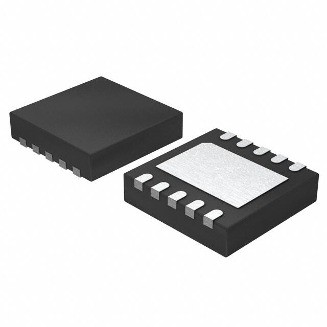
power switches, combined with the tiny 10-pin
MSOP or 3mm x 3mm QFN packages, provide
a solution requiring a minimum of board space.
QFN package is recommended if output current
is higher than 1.5A.
EVALUATION BOARD REFERENCE
Board Number
Dimensions
EV2108DQ/DK-00A
2.5”X x 2.0”Y x 0.5”Z
2A Output Current
Synchronous Rectification
Internal 160mΩ and 190mΩ Power Switches
Input Range of 2.6V to 6V
Over 95% Efficiency
Under Voltage Lockout Protection
Soft-Start Operation
Thermal Shutdown
Internal Current Limit (Source & Sink)
Tiny 10-Pin MSOP and 3x3 QFN Packages
APPLICATIONS
SOHO Routers, PCMCIA Cards, Mini PCI
Handheld Computers, PDAs
Cell phones, Digital Still and Video Cameras
Small LCD Displays
“MPS” and “The Future of Analog IC Technology” are Registered Trademarks of
Monolithic Power Systems, Inc.
TYPICAL APPLICATION
100
VOUT=2.5V
90
6
8
VIN
BST
LX
RUN
SS
COMP
VREF
9
FB
SGND PGND
5
4
3
7
EFFICIENCY (%)
10
80
1
2
VOUT=1.2V
70
60
50
40
30
20
10
0
0.01
MP2108 Rev 1.3
2/26/2020
VIN=3.3V
0.1
1
LOAD CURRENT (A)
www.MonolithicPower.com
MPS Proprietary Information. Unauthorized Photocopy and Duplication Prohibited.
© 2020 MPS. All Rights Reserved.
10
1
�MP2108 – 2A, 6V, 740KHz SYNCHRONOUS BUCK CONVERTER
PACKAGE REFERENCE
TOP VIEW
TOP VIEW
BST
1
10
RUN
VREF
VIN
2
9
VREF
LX
3
8
COMP
PGND
4
7
FB
SGND
5
6
SS
BST
1
10
RUN
VIN
2
9
LX
3
8
COMP
PGND
4
7
FB
SGND
5
6
SS
EXPOSED PAD
ON BACKSIDE
Part Number*
Package
Temperature
Part Number**
Package***
Temperature
MP2108DK
MSOP10
–40C to +85C
MP2108DQ
QFN10
(3mm x 3mm)
–40C to +85C
*
**
For Tape & Reel, add suffix –Z (eg. MP2108DK–Z)
For RoHS compliant packaging, add suffix –LF (eg.
MP2108DK–LF–Z)
***
For Tape & Reel, add suffix –Z (eg. MP2108DQ–Z)
For RoHS compliant packaging, add suffix –LF (eg.
MP2108DQ–LF–Z)
Recommended for output currents higher than 1.5A
ABSOLUTE MAXIMUM RATINGS (1)
Thermal Resistance (3)
Input Supply Voltage VIN .............................. 6.5V
LX Voltage VLX ......................–0.3V to VIN + 0.3V
BST to LX Voltage ......................... –0.3V to +6V
Voltage on All Other Pins............... –0.3V to +6V
Storage Temperature ............... –55C to +150C
MSOP10 ................................. 150 ...... 65 ... C/W
QFN10 (3mm x 3mm) ............. 50 ....... 12 ... C/W
Recommended Operating Conditions (2)
θJA
θJC
Notes:
1) Exceeding these ratings may damage the device.
2) The device is not guaranteed to function outside of its
operating conditions.
3) Measured on approximately 1” square of 1 oz copper.
Input Supply Voltage VIN ....................... 2.6V to 6
Output Voltage VOUT ........................... 0.9V to 5V
Operating Temperature ............. –40C to +85C
ELECTRICAL CHARACTERISTICS
VIN = 5.0V, TA = +25C, unless otherwise noted.
Parameter
Input Voltage Range
Input Undervoltage Lockout
Input Undervoltage Lockout
Hysteresis
Shutdown Supply Current
Operating Supply Current
VREF Voltage
RUN Input Low Voltage
RUN Input High Voltage
RUN Hysteresis
RUN Input Bias Current
MP2108 Rev 1.3
2/26/2020
Symbol Condition
VIN
VREF
VIL
VHL
Min
2.6
VRUN ≤ 0.3V
VRUN > 2V, VFB = 1.1V
VIN = 2.6V to 6V
Typ
2.2
Units
V
V
100
mV
0.5
1.2
2.4
Max
6
1.0
1.8
0.4
1.5
100
www.MonolithicPower.com
MPS Proprietary Information. Unauthorized Photocopy and Duplication Prohibited.
© 2020 MPS. All Rights Reserved.
1
μA
mA
V
V
V
mV
μA
2
�MP2108 – 2A, 6V, 740KHz SYNCHRONOUS BUCK CONVERTER
ELECTRICAL CHARACTERISTICS (continued)
VIN = 5.0V, TA = +25C, unless otherwise noted.
Parameter
Oscillator
Switching Frequency
Maximum Duty Cycle
Minimum On Time
Error Amplifier
Voltage Gain
Transconductance
COMP Maximum Output Current
FB Regulation Voltage
FB Input Bias Current
Soft-Start
Soft-Start Current
Output Switch On-Resistance
Switch On Resistance
Synchronous Rectifier On Resistance
Switch Current Limit (Source)
Synchronous Rectifier Current Limit
(Sink)
Thermal Shutdown
Symbol Condition
fSW
DMAX
TON
VFB = 0.7V
Min
Typ
Max
Units
620
85
740
920
200
KHz
%
ns
400
450
±40
895
–100
V/V
μA/V
μA
mV
nA
AVEA
GEA
VFB
IFB
875
VFB = 0.9V
ISS
VIN = 5V
VIN = 3V
VIN = 5V
VIN = 3V
2.5
915
2
μA
190
280
160
230
3.5
mΩ
mΩ
mΩ
mΩ
A
350
mA
160
C
PIN FUNCTIONS
Pin #
Name
1
BST
2
VIN
3
LX
4
PGND
5
SGND
6
SS
7
FB
8
COMP
9
VREF
10
RUN
MP2108 Rev 1.3
2/26/2020
Description
Power Switch Boost. BST powers the gate of the high-side N-Channel power MOSFET
switch. Connect a 10nF or greater capacitor between BST and LX.
Internal Power Input. VIN supplies the power to the MP2108 through the internal LDO
regulator. Bypass VIN to PGND with a 10μF or greater capacitor. Connect VIN to the input
source voltage.
Output Switching Node. LX is the source of the high-side N-Channel switch and the drain
of the low-side N-Channel switch. Connect the output LC filter between LX and the output.
Power Ground. PGND is the source of the N-Channel MOSFET synchronous rectifier.
Connect PGND to SGND as close to the MP2108 as possible.
Signal Ground.
Soft-Start Input. Place a capacitor from SS to SGND to set the soft-start period. The
MP2108 sources 2μA from SS to the soft-start capacitor at start-up. As the voltage at SS
rises, the feedback threshold voltage increases to limit inrush current at startup.
Feedback Input. FB is the inverting input of the internal error amplifier. Connect a resistive
voltage divider from the output voltage to FB to set the output voltage.
Compensation Node. COMP is the output of the error amplifier. Connect a series RC
network to compensate the regulation control loop.
Internal 2.4V Regulator Bypass. Connect a 10nF capacitor between VREF and SGND to
bypass the internal regulator. Do not apply any load to VREF.
On/Off Control Input. Drive RUN high to turn on the MP2108, drive RUN low to turn the
MP2108 off. For automatic startup, connect RUN to VIN via a 100kΩ pull-up resistor.
www.MonolithicPower.com
MPS Proprietary Information. Unauthorized Photocopy and Duplication Prohibited.
© 2020 MPS. All Rights Reserved.
3
�MP2108 – 2A, 6V, 740KHz SYNCHRONOUS BUCK CONVERTER
TYPICAL PERFORMANCE CHARACTERISTICS
Circuit of Figure 2, VIN = 5V, VOUT = 2.5V, L1 = 5µH, C1 = 10µF, C2 = 22µF, TA = +25C, unless
otherwise noted.
Efficiency vs
Load Current
100
Peak Current vs
Duty Cycle
70
VOUT=1.2V
60
PEAK CURRENT (A)
80
EFFICIENCY (%)
5.0
VOUT=3.3V
90
VOUT=2.5V
50
40
30
20
10
0.1
1
LOAD CURRENT (A)
4.0
3.5
3.0
2.5
VIN=5V
0
0.01
4.5
2.0
10
Feedback Voltage vs
Die Temperature
0.902
0.900
0.898
0.896
0.894
0.892
0.890
0.888
0.886
0.884
-50 -25 0 25 50 75 100 125 150
DIE TEMPERATURE (OC)
MP2108 Rev 1.3
2/26/2020
20
40
60
80
DUTY CYCLE (%)
100
Switching Frequency vs
Die Temperature
SWITCHING FREQUENCY (KHz)
FEEDBACK VOTLAGE (V)
0.904
0
830
810
790
770
750
730
710
690
670
650
630
-50 -25 0 25 50 75 100 125
DIE TEMPERATURE (OC)
www.MonolithicPower.com
MPS Proprietary Information. Unauthorized Photocopy and Duplication Prohibited.
© 2020 MPS. All Rights Reserved.
4
�MP2108 – 2A, 6V, 740KHz SYNCHRONOUS BUCK CONVERTER
TYPICAL PERFORMANCE CHARACTERISTICS (continued)
Circuit of Figure 2, VIN = 5V, VOUT = 2.5V, L1 = 5µH, C1 = 10µF, C2 = 22µF, TA = +25C, unless
otherwise noted.
0.5A-1A Step Resistive Load
Full Load
No Load
VOUT
AC Coupled
10mV/div.
Load Transient
Steady State Operation
Steady State Operation
VOUT
AC Coupled
10mV/div.
IL
1A/div.
VOUT
AC Coupled
200mV/div.
IL
2A/div.
VSW
5V/div.
IL
1A/div.
VSW
5V/div.
400ns/div.
400ns/div.
Start-up through Enable
Start-up through Enable
Shut-down through Enable
Full Load
No Load
No Load
VOUT
2V/div.
VOUT
1V/div.
VOUT
2V/div.
VEN
2V/div.
VEN
5V/div.
VEN
2V/div.
1ms/div.
100ms/div.
400ms/div.
Shut-down through Enable
Full Load
VOUT
2V/div.
VEN
2V/div.
200ms/div.
MP2108 Rev 1.3
2/26/2020
www.MonolithicPower.com
MPS Proprietary Information. Unauthorized Photocopy and Duplication Prohibited.
© 2020 MPS. All Rights Reserved.
5
�MP2108 – 2A, 6V, 740KHz SYNCHRONOUS BUCK CONVERTER
OPERATION
VIN
VIN
OFF ON
RUN
10
ENABLE
CKT & LDO
REGULATOR
Vdr
CURRENT
SENSE
AMPLIFIER
2.6V to 6V
+
-BST
VREF
2.4V
PWM
COMPARATOR
9
C6
GATE
DRIVE
REGULATOR
C1
2
1
+
--
C7
LX
CONTROL
LOGIC
Vdr
L1
VOUT
3
C2
720KHz
OSCILLATOR
RAMP
VBP
CURRENT
LIMIT
COMPARATOR
+
--
UVLO &
THERMAL
SHUTDOWN
R2
+
--
PGND
SS
4
C5
6
-FB
GM -ERROR
AMPLIFIER
VFB
0.9V
CURRENT
LIMIT
THRESHOLD
5
R1
8
SGND
C4
7
+
COMP
R3
C3
Figure 1—Functional Block Diagram
MP2108 Rev 1.3
2/26/2020
www.MonolithicPower.com
MPS Proprietary Information. Unauthorized Photocopy and Duplication Prohibited.
© 2020 MPS. All Rights Reserved.
6
�MP2108 – 2A, 6V, 740KHz SYNCHRONOUS BUCK CONVERTER
The MP2108 measures the output voltage
through an external resistive voltage divider and
compares it to the internal 0.9V reference to
generate the error voltage at COMP. The
current-mode regulator uses the voltage at
COMP and compares it to the inductor current
to regulate the output voltage. The use of
current-mode regulation improves transient
response and control loop stability.
The average inductor current is controlled by
the voltage at COMP, which in turn, is
controlled by the output voltage. Thus the
output voltage controls the inductor current to
satisfy the load.
Since the high-side N-Channel MOSFET
requires voltage above VIN to drive its gate, a
bootstrap capacitor from LX to BST is required
to drive the high-side MOSFET gate. When LX
is driven low (through the low-side MOSFET),
the BST capacitor is internally charged. The
voltage at BST is applied to the high-side
MOSFET gate to turn it on. Voltage is
maintained until the high-side MOSFET is
turned off and the low-side MOSFET is turned
on, and the cycle repeats. Connect a 10nF or
greater capacitor from BST to SW to drive the
high-side MOSFET gate.
At the beginning of each cycle, the high-side
N-Channel MOSFET is turned on, forcing the
inductor current to rise. The current at the drain
of the high-side MOSFET is internally
measured and converted to a voltage by the
current sense amplifier.
That voltage is compared to the error voltage at
COMP. When the inductor current rises
sufficiently, the PWM comparator turns off the
high-side switch and turns on the low-side
switch; forcing the inductor current to decrease.
APPLICATION INFORMATION
1
2
10
6
8
VIN
BST
LX
RUN
SS
COMP
VREF
9
FB
3
7
SGND PGND
5
4
Figure 2—Typical Application Circuit
Internal Low-Dropout Regulator
The internal power to the MP2108 is supplied
from the input voltage (VIN) through an internal
2.4V low-dropout linear regulator, whose output
is VREF. Bypass VREF to SGND with a 10nF
or greater capacitor for proper operation. The
internal regulator can not supply more current
than is required to operate the MP2108.
Therefore, do not apply any external load to
VREF.
MP2108 Rev 1.3
2/26/2020
Soft-Start
The MP2108 includes a soft-start timer that
slowly ramps the output voltage at startup to
prevent excessive current at the input.
When power is applied to the MP2108, and
RUN is asserted. A 2μA internal current source
charges the external capacitor at SS. As the
capacitor charges, the voltage at SS rises. The
MP2108 internally limits the feedback threshold
voltage at FB to that of the voltage at SS. This
forces the output voltage to rise at the same
www.MonolithicPower.com
MPS Proprietary Information. Unauthorized Photocopy and Duplication Prohibited.
© 2020 MPS. All Rights Reserved.
7
�MP2108 – 2A, 6V, 740KHz SYNCHRONOUS BUCK CONVERTER
rate as the voltage at SS, forcing a linear
output voltage ramp from 0V to the desired
regulation voltage during soft-start.
type. All ceramic capacitors should be placed
close to the IC. For most applications, a 10µF
ceramic capacitor will work.
The soft-start period is determined by the
equation:
Selecting the Output Capacitor
The output capacitor (C2) is required to
maintain the DC output voltage. Low ESR
capacitors are preferred to keep the output
voltage ripple to a minimum. The characteristics
of the output capacitor also affect the stability of
the regulation control system. Ceramic,
tantalum, or low ESR electrolytic capacitors are
recommended.
t SS 0.45 C5
Where C5 (in nF) is the soft-start capacitor from
SS to GND, and tSS (in ms) is the soft-start
period. Determine the capacitor required for a
given soft-start period by the equation:
C5 2.22 t SS
Use values for C5 between 10nF and 22nF to
set the soft-start period between 4ms and 10ms.
Setting the Output Voltage (see Figure 2)
Set the output voltage by selecting the resistive
voltage divider ratio. The voltage divider drops
the output voltage to the 0.9V feedback voltage.
Use 10kΩ for the low-side resistor of the
voltage divider. Determine the high-side resistor
by the equation:
V
R2 OUT 1 R1
0
.
9
V
Where R2 is the high-side resistor, R1 is the
low-side resistor and VOUT is the output voltage.
Selecting the Input Capacitor
The input current to the step-down converter is
discontinuous, so a capacitor is required to
supply the AC current to the step-down
converter while maintaining the DC input
voltage. A low ESR capacitor is required to
keep the noise at the IC to a minimum. Ceramic
capacitors are preferred, but tantalum or low
ESR electrolytic capacitors are also an option.
The capacitor can be electrolytic, tantalum or
ceramic. Because it absorbs the input switching
current, it must have an adequate ripple current
rating. Use a capacitor with RMS current rating
greater than 1/2 of the DC load current.
For stable operation, place the input capacitor
as close to the IC as possible. A smaller high
quality 0.1μF ceramic capacitor may be placed
closer to the IC with the larger capacitor placed
further away.
The output voltage ripple is:
VRIPPLE
VOUT
V
1 OUT
f SW L
VIN
1
R ESR
8 f SW C2
Where VRIPPLE is the output voltage ripple, fSW is
the switching frequency, VIN is the input voltage
and RESR is the equivalent series resistance of
the output capacitors.
Choose an output capacitor to satisfy the output
ripple requirements of the design. A 22μF
ceramic capacitor is suitable for most
applications.
Selecting the Inductor
The inductor is required to supply constant
current to the output load while being driven by
the switched input voltage. A larger value
inductor results in less ripple current that in turn
results in lower output ripple voltage. However,
the larger value inductor is likely to have a
larger physical size and higher series
resistance. Choose an inductor that does not
saturate under the worst-case load conditions.
A good rule for determining the inductance is to
allow peak-to-peak ripple current to be
approximately 30% to 40% of the maximum
load current. Make sure that the peak inductor
current (the load current plus half the peak-topeak inductor ripple current) is below 2.5A to
prevent loss of regulation due to the current
limit.
If using this technique, it is recommended that
the larger capacitor be a tantalum or electrolytic
MP2108 Rev 1.3
2/26/2020
www.MonolithicPower.com
MPS Proprietary Information. Unauthorized Photocopy and Duplication Prohibited.
© 2020 MPS. All Rights Reserved.
8
�MP2108 – 2A, 6V, 740KHz SYNCHRONOUS BUCK CONVERTER
Calculate the required inductance value by the
equation:
L
VOUT VIN VOUT
VIN fSW I
Where ∆I is the peak-to-peak inductor ripple
current. It is recommended to choose ∆I to be
30%~40% of the maximum load current.
Compensation
The system stability is controlled through the
COMP pin. COMP is the output of the internal
transconductance error amplifier. A series
capacitor-resistor combination sets a pole-zero
combination to control the characteristics of the
control system.
The DC loop gain is:
V
A VDC FB
VOUT
A VEA G CS R LOAD
Where VFB is the feedback voltage, 0.9V, AVEA
is the transconductance error amplifier voltage
gain, 400 V/V and GCS is the current sense
transconductance, (roughly the output current
divided by the voltage at COMP), 4.5A/V.
RLOAD is the load resistance:
R LOAD
VOUT
I OUT
Where IOUT is the output load current.
The system has 2 poles of importance, one is
due to the compensation capacitor (C3), and
the other is due to the load resistance and the
output capacitor (C2), where:
fP1
G EA
2 A VEA C3
P1 is the first pole, and GEA is the error amplifier
transconductance (450μA/V) and
fP 2
1
2 R LOAD C2
The system has one zero of importance, due to
the compensation capacitor (C3) and the
compensation resistor (R3). The zero is:
f Z1
MP2108 Rev 1.3
2/26/2020
1
2 R3 C3
If large value capacitors with relatively high
equivalent-series-resistance (ESR) are used,
the zero due to the capacitance and ESR of the
output capacitor can be compensated by a third
pole set by R3 and C4. The pole is:
f P3
1
2 R3 C4
The system crossover frequency (the frequency
where the loop gain drops to 1dB or 0dB) is
important. Set the crossover frequency below
one tenth of the switching frequency to insure
stable operation. Lower crossover frequencies
result in slower response and worse transient
load recovery. Higher crossover frequencies
degrade the phase and/or gain margins and
can result in instability.
Table 1—Compensation Values for Typical
Output Voltage/Capacitor Combinations
VOUT
C2
22μF
Ceramic
22μF
2.5V
Ceramic
22μF
3.3V
Ceramic
1.8V
R3
R2
R1
10kΩ 10kΩ
9.1kΩ 2.2nF None 17.8kΩ 10kΩ
12kΩ
13kΩ
47μF
2.5V Tantalum
(300mΩ)
18kΩ
47μF
3.3V Tantalum
(300mΩ)
24kΩ
47μF
Ceramic
47μF
1.2V
Ceramic
C4
6.8kΩ 3.3nF None
47μF
1.8V Tantalum
(300mΩ)
1V
C3
1.8nF None
2nF
1nF
27kΩ 10kΩ
10kΩ 10kΩ
1.2nF 750pF 17.8kΩ 10kΩ
1nF
560pF 27kΩ 10kΩ
6.98kΩ 3.3nF None 1.18kΩ 10kΩ
6.98kΩ 3.3nF None
3.4kΩ 10kΩ
Choosing the Compensation Components
The values of the compensation components
listed in Table 1 yields a stable control loop for
the given output voltage and capacitor. To
optimize the compensation components for
conditions not listed in Table 1, use the
following procedure.
www.MonolithicPower.com
MPS Proprietary Information. Unauthorized Photocopy and Duplication Prohibited.
© 2020 MPS. All Rights Reserved.
9
�MP2108 – 2A, 6V, 740KHz SYNCHRONOUS BUCK CONVERTER
Choose the compensation resistor to set the
desired crossover frequency. Determine the
value by the following equation:
R3
2 C2 f C VOUT
G EA G CS
VFB
Where GEA is the EA transconductance
(450µA/V) and fC is the desired crossover
frequency (preferably 33KHz).
Choose the compensation capacitor to set the
zero below one fourth of the crossover
frequency. Determine the value by the following
equation:
C3
External Bootstrap Diode
An external bootstrap diode may enhance the
efficiency of the regulator, the applicable
conditions of external BST diode are:
VOUT is 5V or 3.3V; and
Duty cycle is high: D=
VOUT
>65%
VIN
In these cases, an external BST diode is
recommended from the output of the voltage
regulator to BST pin, as shown in Fig.3
External BST Diode
IN4148
BST
MP2108
2
R3 f C
SW
CBST
L
5V or 3.3V
COUT
Determine if the second compensation
capacitor, C4 is required. It is required if the
ESR zero of the output capacitor happens at
less than half of the switching frequency or:
Figure 3—Add Optional External Bootstrap
Diode to Enhance Efficiency
C2 R ESR f SW 1
The recommended external BST diode is
IN4148, and the BST cap is 0.1~1µF.
where RESR is the equivalent series resistance
of the output capacitor.
The second compensation
determined by the equation:
C4
capcacitor
is
C2 R ESR(max)
R3
Where RESR(MAX) is the maximum ESR of the
output capacitor.
MP2108 Rev 1.3
2/26/2020
PCB Layout Guide
PCB layout is very important to achieve stable
operation. It is highly recommended to duplicate
EVB layout for optimum performance.
If change is necessary, please follow these
guidelines and take Figure 4 for reference.
1)
Keep the path of switching current short
and minimize the loop area formed by Input
cap, high-side MOSFET and low-side
MOSFET.
2)
Bypass ceramic capacitors are suggested
to be put close to the Vin Pin.
3)
Ensure all feedback connections are short
and direct. Place the feedback resistors
and compensation components as close to
the chip as possible.
4)
Route SW away from sensitive analog
areas such as FB.
5)
Connect IN, SW, and especially GND
respectively to a large copper area to cool
the chip to improve thermal performance
and long-term reliability.
www.MonolithicPower.com
MPS Proprietary Information. Unauthorized Photocopy and Duplication Prohibited.
© 2020 MPS. All Rights Reserved.
10
�MP2108 – 2A, 6V, 740KHz SYNCHRONOUS BUCK CONVERTER
L1
VOUT
1
SS
FB
10 RUN
7
9 VREF
8 COMP
6
R1
BST
VIN 2
LX 3
4
5
Css
PGND
SGND
COUT
GND
VIN
CBST
CIN
GND
R4
C1
R2
R3
C2
Top Layer
GND
Bottom Layer
Figure 4—PCB Layout (Double Layers)
MP2108 Rev 1.3
2/26/2020
www.MonolithicPower.com
MPS Proprietary Information. Unauthorized Photocopy and Duplication Prohibited.
© 2020 MPS. All Rights Reserved.
11
�MP2108 – 2A, 6V, 740KHz SYNCHRONOUS BUCK CONVERTER
PACKAGE INFORMATION
MSOP10
MP2108 Rev 1.3
2/26/2020
www.MonolithicPower.com
MPS Proprietary Information. Unauthorized Photocopy and Duplication Prohibited.
© 2020 MPS. All Rights Reserved.
12
�MP2108 – 2A, 6V, 740KHz SYNCHRONOUS BUCK CONVERTER
QFN10 (3mm x 3mm)
NOTICE: The information in this document is subject to change without notice. Users should warrant and guarantee that third
party Intellectual Property rights are not infringed upon when integrating MPS products into any application. MPS will not
assume any legal responsibility for any said applications.
MP2108 Rev. 1.3
2/26/2020
www.MonolithicPower.com
MPS Proprietary Information. Unauthorized Photocopy and Duplication Prohibited.
© 2020 MPS. All Rights Reserved.
13
�


 工商网监
湘ICP备2023018690号
工商网监
湘ICP备2023018690号
