MP4030A
TRIAC-Dimmable, Primary-Side-Control
Offline LED Controller with Active PFC
The Future of Analog IC Technology
DESCRIPTION
The MP4030A is a TRIAC-dimmable, primaryside-control, offline LED lighting controller with
active PFC. It can output an accurate LED
current for an isolated lighting application with a
single-stage converter. The proprietary realcurrent-control method can accurately control the
LED current using primary-side information. It
can significantly simplify LED lighting system
design by eliminating secondary-side feedback
components and the optocoupler.
The
MP4030A
implements
power-factor
correction and works in boundary-conduction
mode to reduce MOSFET switching losses.
The MP4030A has an integrated charging circuit
at the supply pin for fast start-up without a
perceptible delay.
The proprietary dimming control expands the
TRIAC-based dimming range.
The MP4030A features multiple protections
including over-voltage protection (OVP), shortcircuit protection (SCP), primary-side overcurrent protection (OCP), supply-pin undervoltage lockout (UVLO), and over temperature
protection (OTP). All of which not only simplifies
circuit design but also enhances system reliability
and safety greatly. All fault protections feature
auto-restart.
FEATURES
•
•
•
•
•
•
•
•
•
•
•
•
Primary-Side-Control without Requiring a
Secondary-Side Feedback Circuit
Internal Charging Circuit at the Supply Pin for
Fast Start-Up
Accurate Line & Load Regulation
High Power Factor and Improved THD
Flicker-Free, Phase-Controlled TRIAC
Dimming with Expanded Dimming Range 1%
to 100% Full Range
Operates in Boundary Conduction Mode
Cycle-by-Cycle Current Limit
Primary-Side, Over-Current Protection
Over-Voltage Protection
Short-Circuit Protection
Over-Temperature Protection
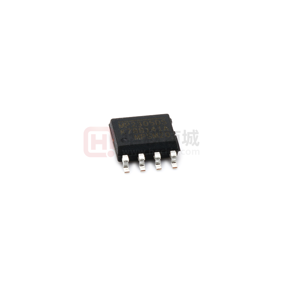
Available in an 8-Pin SOIC Package
APPLICATIONS
•
Solid-State Lighting, including:
• Industrial and Commercial Lighting
• Residential Lighting
All MPS parts are lead-free and adhere to the RoHS directive. For MPS green
status, please visit MPS website under Products, Quality Assurance page.
“MPS” and “The Future of Analog IC Technology” are registered trademarks of
Monolithic Power Systems, Inc.
The MP4030A is available in an 8-pin SOIC
package.
MP4030A Rev.1.01
www.MonolithicPower.com
9/27/2013
MPS Proprietary Information. Patent Protected. Unauthorized Photocopy and Duplication Prohibited.
© 2013 MPS. All Rights Reserved.
1
�MP4030A—PRIMARY-SIDE-CONTROL, OFFLINE, LED CONTROLLER WITH PFC
TYPICAL APPLICATION
A
MP4030A Rev.1.01
www.MonolithicPower.com
9/27/2013
MPS Proprietary Information. Patent Protected. Unauthorized Photocopy and Duplication Prohibited.
© 2013 MPS. All Rights Reserved.
2
�MP4030A—PRIMARY-SIDE-CONTROL, OFFLINE, LED CONTROLLER WITH PFC
ORDERING INFORMATION
Part Number*
Package
SOIC8
MP4030AGS
Top Marking
MP4030A
* For Tape & Reel, add suffix –-Z (e.g. MP4030AGS–Z);
PACKAGE REFERENCE
SOIC8
(4)
ABSOLUTE MAXIMUM RATINGS (1)
Thermal Resistance
VCC Pin Voltage ...........................-0.3V to +30V
Low-Side MOSFET Drain Voltage -0.3V to +30V
ZCD Pin Voltage ................................-8V to +7V
Other Analog Inputs and Outputs .....-0.3V to 7V
ZCD Pin Current ..........................-5mA to +5mA
(2)
Continuous Power Dissipation
(TA = +25°C)
SOIC8 ........................................................ 1.3W
Junction Temperature ...............................150°C
Lead Temperature ....................................260°C
Storage Temperature............... -65°C to +150°C
SOIC8 ....................................96 ...... 45 ... °C/W
Recommended Operating Conditions
(3)
θJA
θJC
Notes:
1) Exceeding these ratings may damage the device.
2) The maximum allowable power dissipation is a function of the
maximum junction temperature TJ(MAX), the junction-toambient thermal resistance θJA, and the ambient temperature
TA. The maximum allowable continuous power dissipation at
any ambient temperature is calculated by PD(MAX)=(TJ(MAX)TA)/ θJA. Exceeding the maximum allowable power dissipation
will cause excessive die temperature, and the regulator will go
into thermal shutdown. Internal thermal shutdown circuitry
protects the device from permanent damage.
3) The device is not guaranteed to function outside of its
operation conditions.
4) Measured on JESD51-7 4-layer board.
VCC Pin Voltage ...............................11V to 27V
Operating Junction Temp (TJ).. -40°C to +125°C
MP4030A Rev.1.01
www.MonolithicPower.com
9/27/2013
MPS Proprietary Information. Patent Protected. Unauthorized Photocopy and Duplication Prohibited.
© 2013 MPS. All Rights Reserved.
3
�MP4030A—PRIMARY-SIDE-CONTROL, OFFLINE, LED CONTROLLER WITH PFC
ELECTRICAL CHARACTERISTICS
TA = +25°C, unless otherwise noted.
Parameter
Supply Voltage
Symbol
Operating Range
VCC
VCC Upper Level: Internal
Charging Circuit Stops and IC
Turns On
VCC Lower Level: Internal
Charging Circuit Triggers
VCC Re-charge and IC turns off
Level in Fault Condition
Supply Current
VCC Charging Current from D
Quiescent Current
Quiescent Current at Fault
Operating Current
Condition
Min
After turn on
10
Typ
Max
Units
27
V
VCCH
9.4
10
10.5
V
VCCL
8.65
9
9.55
V
Fault condition
6.55
7
7.45
V
VD=16V, VCC=5V
12.5
15
17.5
mA
800
1000
µA
220
300
µA
1
2
mA
3
V
VCCEN
ID_Charge
IQ
No switching, VCC=15V
IQ_Fault
Icc
Fault condition, IC latch,
VCC=15V
fs =70kHz, VCC=15V
VMULT
VCOMP from 1.9V to 4.9V
160
Multiplier
Linear Operation Range
Gain
(5)
K
0
VCOMP=2V, VMULT=0.5V
0.82
1.04
1.24
1/V
VCOMP=2V, VMULT=1.5V
0.86
1.05
1.20
1/V
VCOMP=2V, VMULT=3V
0.91
1.06
1.24
1/V
TRIAC-Dimming OFF Detection
Threshold
TRIAC-Dimming ON Detection
Threshold
VMUL_OFF
0.13
0.15
0.17
V
VMUL_ON
0.32
0.35
0.38
V
TRIAC-Dimming OFF Line-Cycle
Blanking Ratio
DOFF_LEB
25
%
TRIAC Dimming Threshold, DutyCycle Ratio to Disable DP
74.4
75
75.4
%
TRIAC Dimming Hysteresis,
Duty-Cycle Ratio to Disable DP
4.6
5.3
6.0
%
0.22
0.25
0.28
V
150
200
250
µs
0.388
0.403
0.417
V
Dimming Pull-Down MOSFET
Turn-ON Threshold
VMULT_DP_ON
Dimming Pull-Down MOSFET
Turn-OFF Delay Time
tDP_OFF_Delay
Starts at the rising edge
of VMULT=VMULT_ON
Error Amplifier
Reference Voltage
VREF
Transconductance
GEA
150
µA/V
COMP Lower Clamp Voltage
VCOMPL
Max. Source Current
ICOMP+
55
µA
ICOMP-
-270
µA
Max. Sink Current without
Dimmer
1.85
1.9
1.96
MP4030A Rev.1.01
www.MonolithicPower.com
9/27/2013
MPS Proprietary Information. Patent Protected. Unauthorized Photocopy and Duplication Prohibited.
© 2013 MPS. All Rights Reserved.
V
4
�MP4030A—PRIMARY-SIDE-CONTROL, OFFLINE, LED CONTROLLER WITH PFC
ELECTRICAL CHARACTERISTICS (continued)
TA = +25°C, unless otherwise noted.
Parameter
Symbol
Sink Current at TRIAC Dimming OFF
Condition
Min
Typ
Max
Units
ISink_Dim
60
70
80
µA
tLEB
575
685
795
ns
Current Sense Comparator
Leading-Edge-Blanking Time
Leading-Edge-Blanking Time for
OCP
tLEB_OCP
0.7
tLEB
VOCP
2.63
2. 73
2.83
V
Current-Sense Upper Clamp Voltage
VS_Clamp_H
2.2
2. 3
2.4
V
Current-Sense Lower Clamp Voltage
VS_Clamp_L
0.08
0.1
0.13
V
0.32
0.35
0.38
V
510
550
590
mV
1.8
2.5
3.1
µs
0.85
1.2
1.5
µs
5.1
5.4
5.7
V
1.35
1.85
2.35
µs
OCP Threshold
Zero-Current Detector
Zero-Current Detection Threshold
VZCD_T
Zero-Current Detection Hysteresis
VZCD_HY
tZCD_LEB
Zero-Current Detection LEB
Falling Edge
Starts at Gate Turn Off,
VS≥0.25
Starts at Gate Turn Off,
VS 0.5 ⋅ VCO _PP .
Optional Protection Circuit
In large output voltage or large LEDs current
application, MOSFET M may be destroyed by
over-voltage or over-current when LED+ shorted
to LED- at working.
Gate-Source (GS) Over-voltage Protection:
DO
NS
D
RO +
R
M
DG
DZ RG
CO
C
+
Figure 15: Gate-Source OVP Circuit
Figure14: Ripple Suppressor
Principle:
Shown in Figure 14, Resister R, capacitor C, and
MOSFET M compose the ripple suppressor.
Through the RC filter, C gets the mean value of
the output voltage VCo to drive the MOSFET M. M
works in variable resistance area. C’s voltage VC
is steady makes the LEDs voltage is steady, so
the LEDs current will be smooth. MOSFET M
holds the ripple voltage vCo of the output.
Diode D and Zener diode DZ are used to restrain
the overshoot at start-up. In the start-up process,
through D and DZ, C is charged up quickly to turn
on M, so the LED current can be built quickly.
When VC rising up to about the steady value, D
and DZ turn off, and C combines R as the filter to
get the mean voltage drop of VCo.
The most important parameter of MOSFET M is
the threshold voltage Vth which decides the
power loss of the ripple suppressor. Lower Vth is
better if the MOSFET can work in variable
resistance area. The BV of the MOSFET can be
selected as double as VCo and the Continues
Drain current level can be selected as decuple as
the LEDs’ current at least.
Figure 15 shows GS over-voltage protection
circuit. Zener diode DG and resistor RG are used
to protect MOSFET M from GS over-voltage
damaged. When LED+ shorted to LED- at normal
operation, the voltage drop on capacitor C is high,
and the voltage drop on Gate-Source is the same
as capacitor C. The Zener diode DG limits the
voltage VGS and RG limits the charging current to
protect DG. RG also can limit the current of DZ at
the moment when LED+ shorted to LED-. VDG
should bigger than Vth.
Drain-Source Over-voltage and Over-current
Protection
As Figure 16 shows, NPN transistor T, resistor
RC and RE are set up to protect MOSFET M from
over-current damaged when output short occurs
at normal operation. When LED+ shorted to LED-,
the voltage vDS of MOSFET is equal to the vCo
which has a high surge caused by the parasitic
parameter. Zener Dioder DDS protects MOSFET
from over-voltage damaged. Transistor T is used
to pull down the VGS of M. When M turns off, the
load is opened, MP4030A detects there is an
OVP happened, so the IC functions in quiescent.
MP4030A Rev.1.01
www.MonolithicPower.com
9/27/2013
MPS Proprietary Information. Patent Protected. Unauthorized Photocopy and Duplication Prohibited.
© 2013 MPS. All Rights Reserved.
17
�MP4030A—PRIMARY-SIDE-CONTROL, OFFLINE, LED CONTROLLER WITH PFC
The pull down point is set by RC and RE:
MOSFET LIST
In the Table 1, there are some recommended
MOSFET for ripple suppressor.
VC
RE
⋅ O = 0.7 V
RC + RE 2
RC DDS RE
T
DO
NS
RO
D M
+ R
CO
C
DZ
RG
+
Figure 16: Drain-Source OVP and OCP Circuit
Manufacture P/N
Si4446DY
FTD100N10A
P6015CDG
Manufacture
Vishay
IPS
NIKO-SEM
Table 1: MOSFET LIST
VDS/ID
Vth(VDS=VGS@TJ=25°C)
40V/3A
0.6-1.6V@ Id=250μA
100V/17A
1.0-2.0V@ Id=250μA
150V/20A
0.45-1.20V@ Id=250μA
MP4030A Rev.1.01
www.MonolithicPower.com
9/27/2013
MPS Proprietary Information. Patent Protected. Unauthorized Photocopy and Duplication Prohibited.
© 2013 MPS. All Rights Reserved.
Power Stage


 工商网监
湘ICP备2023018690号
工商网监
湘ICP备2023018690号

