MP24895
Step-down White-LED Driver
Wide 6-36V Input Voltage
The Future of Analog IC Technology
DESCRIPTION
FEATURES
The MP24895 is step-down LED driver, which
is designed in continuous current mode for
driving the high-brightness LEDs from a wide
input voltage of 6V to 36V.
•
•
•
•
•
•
•
•
•
The MP24895 employs a hysteretic control
scheme to regulate LED current. Moreover, the
control scheme provides optimal loop
stabilization and a very quick response time.
For a high accuracy, the MP24895 senses LED
current by an external high-side resistor. Its low
100mV average feedback voltage reduces
power loss and improves the efficiency.
Internal 36V MOSFET
Wide 6V-to-36V Input Range
1A Output Current
High Efficiency
Hysteretic Control
PWM and Analog Dimming
1000:1 PWM Dimming Resolution
UVLO, Thermal Shutdown
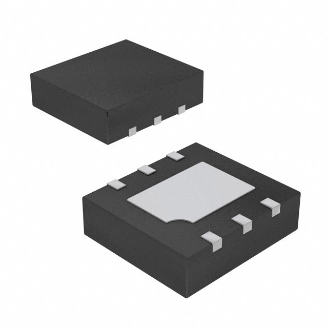
Available in TSOT23-5 and
Packages
QFN-6
APPLICATIONS
•
•
•
•
•
The MP24895 implements PWM and analog
dimming together on the EN/DIM pin.
The MP24895 includes under-voltage lockout,t
and thermal overload protection to prevent
damage in the event of an output overload.
Low-Voltage Halogen Replacement
Low-Voltage General Illumination
Automotive/Decorative LED Lighting
Signs/Emergency Lighting
LED Backlighting
All MPS parts are lead-free and adhere to the RoHS directive. For MPS green
status, please visit MPS website under Products, Quality Assurance page.
The MP24895 is available in TSOT23-5 and
QFN-6 packages.
“MPS” and “The Future of Analog IC Technology” are registered trademarks of
Monolithic Power Systems, Inc.
TYPICAL APPLICATION
D
VIN
6 – 36V
R SENSE
CIN
IN
RS
L
MP24895
EN/DIM
MP24895 Rev. 1.0
8/6/2015
GND
SW
www.MonolithicPower.com
MPS Proprietary Information. Patent Protected. Unauthorized Photocopy and Duplication Prohibited.
© 2015 MPS. All Rights Reserved.
1
�MP24895 – STEP-DOWN WHITE-LED DRIVER WITH 6-36V INPUT VOLTAGE
ORDERING INFORMATION
Part Number*
Top Marking
MP24895GJ*
Package
TSOT23-5
MP24895GQ**
QFN-6 (3x3mm)
AKD
AKD
* For Tape & Reel, add suffix –Z (e.g. MP24895GJ–Z);
* *For Tape & Reel, add suffix –Z (e.g. MP24895GQ–Z);
PACKAGE REFERENCE
TSOT23-5
QFN-6 (3x3mm)
ABSOLUTE MAXIMUM RATINGS (1)
Thermal Resistance
VIN, VSW ........................................ -0.3V to +40V
VRS ................................................. VIN-5V to VIN
All Other Pins .............................. -0.3V to +6.3V
Continuous Power Dissipation (TA = +25°C) (2)
TSOT23-5 ..................................................1.1W
QFN-6 (3x3mm) .........................................2.5W
Junction Temperature .............................. 150°C
Lead Temperature ................................... 260°C
Storage Temperature ............... -65°C to +150°C
TSOT23-5 ............................ 110 ..... 55 ... °C/W
QFN-6 (3x3mm) .................... 50 ...... 14 ... °C/W
Recommended Operating Conditions
(3)
Supply Voltage VIN ............................. 6V to 36V
Operating Junction Temp. (TJ). ... -40°C to +125°C
MP24895 Rev. 1.0
8/6/2015
(4)
θJA
θJC
Notes:
1) Exceeding these ratings may damage the device.
2) The maximum allowable power dissipation is a function of the
maximum junction temperature TJ(MAX), the junction-toambient thermal resistance θJA, and the ambient temperature
TA. The maximum allowable continuous power dissipation at
any ambient temperature is calculated by PD(MAX)=(TJ(MAX)TA)/ θJA. Exceeding the maximum allowable power dissipation
will cause excessive die temperature, and the regulator will go
into thermal shutdown. Internal thermal shutdown circuitry
protects the device from permanent damage.
3) The device is not guaranteed to function outside of its
operation conditions.
4) Measured on JESD51-7 4-layer board.
www.MonolithicPower.com
MPS Proprietary Information. Patent Protected. Unauthorized Photocopy and Duplication Prohibited.
© 2015 MPS. All Rights Reserved.
2
�MP24895 – STEP-DOWN WHITE-LED DRIVER WITH 6-36V INPUT VOLTAGE
ELECTRICAL CHARACTERISTICS
(6)
VIN = 24V, TJ =-40°C to 125°C , unless otherwise noted.
Parameter
Symbol
Condition
Min
Input Voltage
IN Under-Voltage Lockout
Under-Voltage Lockout Hysteresis
Shutdown Supply Current
Quiescent Supply Current
VIN
VIN UVLO
VIN Rising
6
4.7
ISD
IQ
No Switching
Feedback Reference Voltage
(with respect to VIN)
VIN-VRS
ForTj=25°C,
VEN/DIM=1.28V
EN/DIM Enable High Voltage
VEN
For Tj=-40°C to 125°C
VEN/DIM=1.28V
VEN Rising
EN/DIM Enable Hysteresis
EN/DIM Pull-Up Resistor
Internal Reference Voltage
Switch On Resistance
(5)
Minimum On Time
VEN HYS
REN
VREF
RDS ON
tON MIN
(5)
Minimum Off Time
(5)
Thermal Shutdown Temperature
Thermal Shutdown Hysteresis
(5)
HIGH
94
Typ
Max
Units
36
5.9
5.3
700
170
0.7
250
1.1
V
V
mV
µA
mA
100
106
mV
108
mV
92
0.19
0.25
0.31
V
90
1.24
50
45
1.28
0.2
100
mV
kΩ
V
Ω
ns
VEN/DIM=0.3V
1.32
0.4
tOFF_MIN
80
ns
TOTP
150
°C
TOTP HYS
15
°C
Notes:
5) Guaranteed by design
6) Not test in production, guaranteed by characterization. Typical value represent the most likely parametric norm at +25°C
MP24895 Rev. 1.0
8/6/2015
www.MonolithicPower.com
MPS Proprietary Information. Patent Protected. Unauthorized Photocopy and Duplication Prohibited.
© 2015 MPS. All Rights Reserved.
3
�MP24895 – STEP-DOWN WHITE-LED DRIVER WITH 6-36V INPUT VOLTAGE
TYPICAL CHARACTERISTICS
VIN =18V, VOUT =10V, L =47µH, TA = 25°C, unless otherwise noted.
VIN UVLO
EN UVLO
VRS
101.0
0.250
5.50
100.8
5.45
100.6
0.248
5.40
100.4
5.25
5.20
0.246
VRS(mV)
5.30
UVLO(V)
UVLO(V)
5.35
0.244
100.2
100.0
99.8
99.6
5.15
5.10
99.4
0.242
99.2
5.05
5.00
-60 -40 -20 0 20 40 60 80100120140
0.240
-60 -40 -20 0 20 40 60 80100 120140
RDSON
99.0
-60 -40 -20 0 20 40 60 80 100120140
Reference Voltage
0.50
1.280
0.45
0.40
1.278
0.35
VREF(V)
0.30
0.25
0.20
1.276
1.274
0.15
0.10
1.272
0.05
0
-60 -40 -20 0 20 40 60 80 100120140
MP24895 Rev. 1.0
8/6/2015
1.270
-60 -40 -20 0 20 40 60 80 100120 140
www.MonolithicPower.com
MPS Proprietary Information. Patent Protected. Unauthorized Photocopy and Duplication Prohibited.
© 2015 MPS. All Rights Reserved.
4
�MP24895 – STEP-DOWN WHITE-LED DRIVER WITH 6-36V INPUT VOLTAGE
TYPICAL PERFORMANCE CHARACTERISTICS (continued)
VIN = 18V, VOUT = 10V, L =47µH, TA = 25ºC, unless otherwise noted.
Analog Dimming
1000
98
900
96
800
LED CURRENT (mA)
100
94
92
90
88
86
84
82
80
10
PWM Dimming
1200
LED CURRENT (mA)
Efficiency Test
700
600
500
400
300
200
MP24895 Rev. 1.0
8/6/2015
20
25
VIN (V)
30
35
0
0
800
600
400
200
100
15
1000
0.5
1
1.5
VADIM (V)
2
2.5
0
0 10 20 30 40 50 60 70 80 90100110
www.MonolithicPower.com
MPS Proprietary Information. Patent Protected. Unauthorized Photocopy and Duplication Prohibited.
© 2015 MPS. All Rights Reserved.
5
�MP24895 – STEP-DOWN WHITE-LED DRIVER WITH 6-36V INPUT VOLTAGE
TYPICAL PERFORMANCE CHARACTERISTICS (continued)
VIN = 18V, VOUT = 10V, L =47µH, TA = 25ºC, unless otherwise noted.
Steady State
VIN Start-up
VSW
10V/div.
VSW
10V/div.
IL
500mA/div.
VEN/DIM
2V/div.
VSW
10V/div.
VEN/DIM
1V/div.
VIN
10V/div.
IL
1A/div.
ILED
500mA/div.
IL
500mA/div.
Analog Dimming
PWM Dimming
VEN/DIM = 0.9V
fPWM = 2kHz, DPWM = 50%
VSW
10V/div.
VSW
10V/div.
VPWM
5V/div.
IL
500mA/div.
IL
500mA/div.
Short Protection
VSW
10V/div.
VEN/DIM
1V/div.
VEN/DIM
500mV/div.
VIN
20V/div.
VEN Start-up
IL
500mA/div.
Open Protection
Over-Temperature
Protection
TA = 125 C
VSW
10V/div.
VSW
10V/div.
IL
500mA/div.
ILED
500mA/div.
MP24895 Rev. 1.0
8/6/2015
www.MonolithicPower.com
MPS Proprietary Information. Patent Protected. Unauthorized Photocopy and Duplication Prohibited.
© 2015 MPS. All Rights Reserved.
6
�MP24895 – STEP-DOWN WHITE-LED DRIVER WITH 6-36V INPUT VOLTAGE
PIN FUNCTIONS
TSOT23-5
Pin#
QFN-6
(3x3mm)
Pin#
1
1
SW
2
2
GND
Name Description
Drain of Internal MOSFET. Connect the inductor common terminal and
Schottky anode to this pin.
Ground.
Enable/Dimming Command Input. For PWM dimming, apply a square wave
signal to this pin. For analog dimming, apply a 0.3V-to-2.5V DC voltage to
EN/DIM linearly control the LED current range from 25% to 200%. Turn off the output
current when pulling this pin below 0.2V. Leave it open for normal operation
(VEN/DIM=1.28V).
3
5
4
4
RS
LED Current Sense Input. Connect a current-sense resistor to program the
LED average current to IN pin.
5
3
IN
Input Supply Pin. Connect an appropriate decoupling capacitor from the IN
pin to GND.
6
N/C
MP24895 Rev. 1.0
8/6/2015
Not Connected.
www.MonolithicPower.com
MPS Proprietary Information. Patent Protected. Unauthorized Photocopy and Duplication Prohibited.
© 2015 MPS. All Rights Reserved.
7
�MP24895 – STEP-DOWN WHITE-LED DRIVER WITH 6-36V INPUT VOLTAGE
FUNCTION DIAGRAM
D
VIN
Rsense
CIN
IN
RS
HV Regulator 5V
1.275V
Reference
High Side
Current Sense
L
SW
0.2V
Enable
+
DIM
EN /DIM
Filter
PWM
+
Driver
R1
R2
GND
Figure 1: MP24895 Functional Block Diagram
MP24895 Rev. 1.0
8/6/2015
www.MonolithicPower.com
MPS Proprietary Information. Patent Protected. Unauthorized Photocopy and Duplication Prohibited.
© 2015 MPS. All Rights Reserved.
8
�MP24895 – STEP-DOWN WHITE-LED DRIVER WITH 6-36V INPUT VOLTAGE
OPERATION
Steady State
The MP24895 is a hysteretic-controlled, stepdown LED driver that is easily configured for
various applications with an input range from 6V
to 36V. The converter employs a high-side
current-sense resistor to detect and regulate the
LED current. The voltage across the currentsense resistor is measured and regulated to
within 100mV±20mV.
The internal 1.275V reference voltage provides a
0.2V reference to enable the part and a 1.275V
pull-up voltage as current reference. When
VEN>0.2V, the output of the comparator goes high
and the other blocks are enabled.
System Soft Start
The voltage on the EN/DIM pin is the inductor
current reference. An external capacitor from the
EN/DIM pin to ground provides a soft-start delay.
When VIN starts, internal voltage source charges
the capacitor from 0V to 1.25V for soft-start.
Dimming Control
MP24895 provides two dimming methods: PWM
dimming and DC analog dimming.
To use PWM dimming, apply a square wave to
the EN/DIM pin. To use analog dimming, apply a
0.3V-to-2.5V DC voltage to this pin.
A high-side resistor, RSENSE, senses the output
current. When the switch is on, R2 is shorted and
R1 sets the output current upper-threshold.
When the switch is off, R1 and R2 set the output
current lower-threshold, and the ratio of R1 and
R2 determines the current hysteresis.
Enable Control
Once Input voltage is applied, the internal 1.275V
reference is connected to EN/DIM pin through
pull up resistor. If the EN/DIM pin is left open, the
IC automatically starts up to the maximum
brightness. Adding a capacitor to this pin can
hereby program a soft-start time.
Applying an external voltage range from 0.2V to
1.25V to the EN/DIM pin linearly controls the
current-sense voltage reference from 0mV to
100mV for analog dimming.
Applying an external PWM voltage with an
amplitude of 1.25V to the EN/DIM pin achieves
PWM dimming. For additional information on the
flexible external PWM dimming method, please
refer to the “Selecting Dimming Control Mode”
section.
MP24895 Rev. 1.0
8/6/2015
www.MonolithicPower.com
MPS Proprietary Information. Patent Protected. Unauthorized Photocopy and Duplication Prohibited.
© 2015 MPS. All Rights Reserved.
9
�MP24895 – STEP-DOWN WHITE-LED DRIVER WITH 6-36V INPUT VOLTAGE
APPLICATION INFORMATION
Setting the LED Current
The LED current is set by the current-setting
resistor between the IN and RS pins, where:
RSET=100mV/ILED
For RSET=0.2Ω, the LED current is set to 500mA
Selecting the Inductor
Lower value of the inductor results in higher
switching frequencies, leading to larger switch
loss. For most applications, select a switching
frequency between 200kHz and 600kHz.
Estimate the inductor value based on the desired
switching frequency, where:
V
(1- OUT ) × VOUT
VIN
L=
0.4 × ILED × fSW
Selecting Soft-Start Capacitor
The delay time with the soft-start capacitor can
be estimated by 0.2ms/nF. In PWM dimming,
select a C


 工商网监
湘ICP备2023018690号
工商网监
湘ICP备2023018690号
