MP2615A
2 A, 1- or 2- Cell Li-Ion Battery Charger
in 3mm x 3mm Package
The Future of Analog IC Technology
DESCRIPTION
FEATURES
The MP2615A is a high-efficiency, switch mode
battery charger suitable for 1- or 2- cell lithiumion or lithium-polymer applications. The
MP2615A is capable of delivering 2 A of charge
current programmable via an accurate sense
resistor over the entire input range.
•
•
•
•
•
The MP2615A regulates the charge current and
full battery voltage using two control loops to
achieve high-accuracy constant current (CC)
charge and constant voltage (CV) charge.
•
•
•
Constant-off-time
(COT)
control
allows
operation at up to 99% duty cycle when the
battery voltage is close to the input voltage,
ensuring the charge current always remains at
a relatively high level.
The battery temperature and charging status
are always monitored during each charging
cycle. Two status monitor output pins are
provided to indicate the battery charging status
and input power status. Also, the MP2615A
features internal reverse-blocking protection.
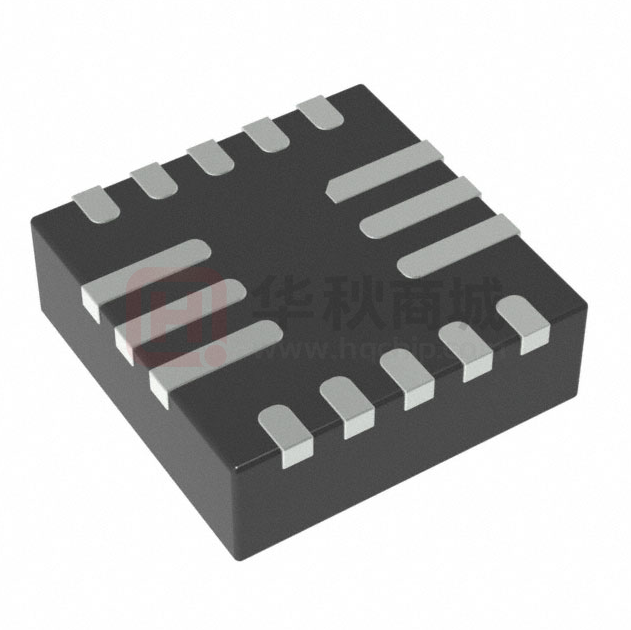
The MP2615A is available in a 3mm × 3mm
16-pin QFN package.
•
•
•
•
•
•
4.75 V to 18 V Operating Input Voltage
Up to 99% Duty Cycle Operation
Up to 2 A Programmable Charging Current
±0.75% Full Battery Voltage Accuracy
4.2 V/Cell and 4.35 V/Cell Selection for Full
Battery Voltage
Fully Integrated Power Switches
Internal Loop Compensation
No External Reverse-Blocking Diode
Required
Preconditioning for Fully Depleted Battery
Charging Operation Indicator
Programmable Safety Timer
Thermal Shutdown Protection
Cycle-by-Cycle Over-Current Protection
Battery Temperature Monitor and Protection
APPLICATIONS
•
•
•
Smart Phones
Portable Hand-Held Solutions
Portable Media Players
All MPS parts are lead-free, halogen-free, and adhere to the RoHS
directive. For MPS green status, please visit the MPS website under
Quality Assurance.
“MPS” and “The Future of Analog IC Technology” are registered
trademarks of Monolithic Power Systems, Inc.
Analog digital adaptive modulation (ADAM) and advanced asynchronous
modulation (AAM) are trademarks of Monolithic Power Systems, Inc.
TYPICAL APPLICATION
Efficiency
100
95
90
85
VIN=5V,1CELL,4.35V/CELL
80
75
70
VIN=18V,2CELL,4.2V/CELL
65
60
0
0.5
MP2615A Rev. 1.0
www.MonolithicPower.com
4/22/2015
MPS Proprietary Information. Patent Protected. Unauthorized Photocopy and Duplication Prohibited.
© 2015 MPS. All Rights Reserved.
1
1.5
IBATT(A)
2
2.5
1
�MP2615A – 2 A, 1- CELL OR 2- CELL LI-ION BATTERY CHARGER
ORDERING INFORMATION
Part Number*
MP2615AGQ
Package
QFN-16 (3mm × 3mm)
Top Marking
See Below
* For Tape & Reel, add suffix –Z (e.g. MP2615AGQ–Z).
TOP MARKING
ANK: Product code of MP2615A
Y: Year code
LLL: Lot number
PACKAGE REFERENCE
MP2615A Rev. 1.0
www.MonolithicPower.com
4/22/2015
MPS Proprietary Information. Patent Protected. Unauthorized Photocopy and Duplication Prohibited.
© 2015 MPS. All Rights Reserved.
2
�MP2615A – 2 A, 1- CELL OR 2- CELL LI-ION BATTERY CHARGER
ABSOLUTE MAXIMUM RATINGS (1)
Thermal Resistance
VSW ...............................................–0.3 V to 23 V
VIN, VACOK, VCHGOK......................................... –0.3 V to 23 V
VBATT,VCSP………………………… –0.3 V to 12 V
VBST ..................................................... VSW + 6 V
All other pins ..................................–0.3 V to 6 V
Junction temperature ................................150°C
Lead temperature......................................260°C
(2)
Continuous power dissipation (TA = +25°C)
............................................................ 2.5 W
Operating temperature.............. –40°C to +85°C
QFN-16 (3mm x 3mm)............ 50 ...... 12... °C/W
Recommended Operating Conditions
(3)
VIN ................................................4.75 V to 18 V
VBATT .................................................2 V to 8.7 V
Operating junction temp. (TJ). . –40°C to +125°C
(4)
θJA
θJC
NOTES:
1) Exceeding these ratings may damage the device.
2) The maximum allowable power dissipation is a function of the
maximum junction temperature TJ (MAX), the junction-toambient thermal resistance θJA, and the ambient temperature
TA. The maximum allowable continuous power dissipation at
any ambient temperature is calculated by PD (MAX) = (TJ
(MAX)-TA)/θJA. Exceeding the maximum allowable power
dissipation produces an excessive die temperature, causing
the regulator to go into thermal shutdown. Internal thermal
shutdown circuitry protects the device from permanent
damage.
3) The device is not guaranteed to function outside of its
operating conditions.
4) Measured on JESD51-7, 4-layer PCB.
MP2615A Rev. 1.0
www.MonolithicPower.com
4/22/2015
MPS Proprietary Information. Patent Protected. Unauthorized Photocopy and Duplication Prohibited.
© 2015 MPS. All Rights Reserved.
3
�MP2615A – 2 A, 1- CELL OR 2- CELL LI-ION BATTERY CHARGER
ELECTRICAL CHARACTERISTICS
VIN = 12 V, VCELL = 0 V, VSEL = 0 V, C1 = 22 µF, C2 = 22 µF, TA = 25°C, unless otherwise noted.
Parameter
Symbol Condition
Min
Typ
Max
Units
4.5
8.75
5
12
18
18
V
3.55
3.75
3.95
V
Input voltage and current
Input voltage
VIN
Under-voltage lockout
threshold rising
Under-voltage lockout
threshold hysteresis
Supply current
Power MOS
High-side switch
resistance
Low-side switch
resistance
on
on
VCELL = 4 V
VCELL = 0 V
VUVLO
225
ISHDN
EN = 4 V, Shutdown current
0.27
IQ
EN = 0 V, Quiescent current
1.1
110
mΩ
RL_DS(ON)
110
mΩ
EN = 4 V, VSW = 0 V
Frequency and time parameter
Switching frequency
FSW
Foldback frequency
Minimum off time (5)
TOFF
Charging parameter
VBATT = 7.5 V
VBATT = 0 V
VBATT = 9 V
Terminal battery voltage VBATT_FULL
over-voltage
Recharge threshold at
VBATT
VBOVP
VRECH
VSEL = 0 V
VSEL = 4 V
VSEL = 0 V
VCELL = 0 V
VSEL=4 V
VCELL = 0 V
VSEL=0 V
VCELL = 4 V
VSEL = 4 V
VCELL = 4 V
VSEL = 0 V
VSEL = 4 V
0
Trickle
hysteresis
VTC
4.35
4.2
4.386
4.252
8.62
8.99
9.36
8.34
8.71
9.08
4.3
4.49
4.67
4.17
4.36
4.54
CC current
Trickle charge current
ICC
ITC
V/Cell
V
VSEL = 0 V
VSEL = 4 V
CC
Trickle
RS1 = 50 mΩ
μA
kHz
kHz
ns
4.328
4.168
charge
Peak current limit
1
760
160
200
Recharge hysteresis
Trickle charge voltage
threshold
mA
RH_DS(ON) Measured from VIN to SW
Switch leakage
Battery
threshold
mV
4.1
4.0
150
3.1
3.0
mV/Cell
225
mV/Cell
V/Cell
V/Cell
3.2
1.8
5%
2.2
2
10%
MP2615A Rev. 1.0
www.MonolithicPower.com
4/22/2015
MPS Proprietary Information. Patent Protected. Unauthorized Photocopy and Duplication Prohibited.
© 2015 MPS. All Rights Reserved.
A
2.2
15%
A
ICC
4
�MP2615A – 2 A, 1- CELL OR 2- CELL LI-ION BATTERY CHARGER
ELECTRICAL CHARACTERISTICS (continued)
VIN = 12 V, VCELL = 0 V, VSEL = 0 V, C1 = 22 µF, C2 = 22 µF, TA = 25°C, unless otherwise noted.
Parameter
Symbol Condition
Termination
current
IBF
threshold
VIN minimum head-room
VIN − VBATT
(reverse blocking)
Maximum
current-sense
VSENSE
voltage (CSP to BATT)
CSP, BATT current
ICSP, IBATT Charging disabled
ACOK/CHGOK open-drain
VDRAIN = 0.3 V
sink current
VCC regulator output
VCC output voltage
VCC
VCC load regulation
∆VCC
ILOAD= 0 to 10 mA
EN control
Min
Typ
Max
Units
5%
10%
15%
ICC
300
90
100
110
mV
3
µA
5
4.25
mA
4.5
EN input low voltage
4.75
10
V
mV
0.4
V
1.8
EN input high voltage
IEN
EN input current
mV
Timer protection
Trickle charge time
tTrickle_tmr
CC/CV charge time
tTotal_tmr
NTC protection
NTC
low
temp
rising
threshold
NTC
low
temp
rising
threshold hysteresis
NTC high temp falling
threshold
NTC low temp falling
threshold hysteresis
Thermal protection
Thermal shutdown(5)
TSHDN
Thermal
shutdown
hysteresis(5)
V
EN = 4 V
4
EN = 0 V
0.2
CTMR = 0.47 μF
CTMR = 0.47 μF
30
165
72
73.3
μA
Mins
74.6
RNTC = NCP18 x 103, 0°C
2
28
29.3
%VCC
30.6
RNTC = NCP18 x 103, 50°C
2
150
°C
20
°C
Reverse leakage blocking
Battery
current
reverse
leakage
ILEAKAGE
VCELL = 0 V
VCELL = 4 V
3
0.5
µA
µA
NOTES:
5) Guaranteed by design.
MP2615A Rev. 1.0
www.MonolithicPower.com
4/22/2015
MPS Proprietary Information. Patent Protected. Unauthorized Photocopy and Duplication Prohibited.
© 2015 MPS. All Rights Reserved.
5
�MP2615A – 2 A, 1- CELL OR 2- CELL LI-ION BATTERY CHARGER
PIN FUNCTIONS
Package
Pin #
Name
1
2
SW
VIN
3
VCC
4
CELL
5
SEL
6
7
8
9
10
EN
NC
AGND
BATT
CSP
On/off control input. EN is pulled to GND with a 1 M internal resistor.
No connection. Please leave NC floating.
Analog ground.
Positive battery terminal.
Battery current sense positive input. Connect a resistor (RS1) between CSP and BATT.
11
CHGOK
Charging complete indicator. A logic low indicates a charging operation. CHGOK will
become an open drain once the charge is completed or suspended.
12
ACOK
13
NTC
14
TMR
15
BST
16
PGND
Description
Switch output.
Power supply voltage.
Coarse regulator output. Internally generated 4.5 V. Bypass with a 1 µF capacitor to
AGND. Used as low-side switch driver and pull-up bias voltage NTC resistivor divider. Do
NOT connect an external load to VCC.
Command input for the number of li-ion cells. Connect CELL to VCC for 1-cell
application; short CELL to AGND for 2-cell application.
Input pin for setting terminal battery voltage:
SEL = Low-level: VBATT = 4.35 V/cell.
SEL = High-level: VBATT =4.2 V/cell.
Valid input supply indicator. A logic low on ACOK indicates the presence of a valid input
power supply.
Thermistor input. Connect a resistor from NTC to VCC and the thermistor from NTC to
ground.
Internal safety timer control. Connect a capacitor from this node to AGND to set the
timer. The timer can be disabled by connecting TMR to AGND directly.
Bootstrap. A capacitor is needed to drive the power switch’s gate above the supply
voltage. It is connected between SW and BST to form a floating supply across the power
switch driver.
Power ground.
MP2615A Rev. 1.0
www.MonolithicPower.com
4/22/2015
MPS Proprietary Information. Patent Protected. Unauthorized Photocopy and Duplication Prohibited.
© 2015 MPS. All Rights Reserved.
6
�MP2615A – 2 A, 1- CELL OR 2- CELL LI-ION BATTERY CHARGER
TYPICAL PERFORMANCE CHARACTERISTICS
VIN = 5 V/9 V, C1 = C2 = 22 µF, SEL = Low/High, CELL = Low/High, L = 6.8 µH, RS1 = 50 mΩ,
battery simulator, TA = 25°C, unless otherwise noted.
Charge Current vs.
Battery Voltage
Charge Current vs.
Battery Voltage
VIN=5V,1 cell
2.5
2.5
Battery Full Voltage vs.
Temperature
VIN=9V,2 cell
1 cell
4.38
1.5
1
0.5
4.34
2
4.32
VBATT(V)
CHARGE CURRENT(A)
CHARGE CURRENT(A)
4.36
2
1.5
1
4.3
V BATT_FULL =4.35V
4.28
4.26
4.24
V BATT_FULL =4.2V
4.22
0.5
4.2
0
0
1
2
3
4
BATTERY VOLTAGE(V)
0
5
0
2
4
6
8
BATTERY VOLTAGE(V)
4.18
-50
10
0
50
100
150
0
50
100
150
8.8
2 cell
2.09
CC CHARGE CURRENT (A)
8.75
8.7
VBATT(V)
8.65
V BATT_FULL =8.7V
8.6
8.55
8.5
V BATT_FULL =8.4V
8.45
8.4
8.35
-50
0
50
100
2.07
2.05
2.03
2.01
1.99
1.97
1.95
-50
150
0
50
100
150
TRICKLE CHARGE CURRENT (mA)
Battery Full Voltage vs.
Temperature
230
220
210
200
190
180
170
160
-50
220
4.5
210
4.49
200
Auto-Recharge Threshold
vs. Temperature
1 cell
4.15
4.1
180
VRCH(V)
4.48
190
VCC(V)
CHARGE FULL CURRENT (mA)
VCC Output vs.
Temparature
4.47
4.46
170
160
4.45
150
-50
4.44
-50
0
50
100
150
4.35V/cell
4.05
4
3.95
4.2V/cell
0
50
100
150
3.9
-50
0
50
MP2615A Rev. 1.0
www.MonolithicPower.com
4/22/2015
MPS Proprietary Information. Patent Protected. Unauthorized Photocopy and Duplication Prohibited.
© 2015 MPS. All Rights Reserved.
100
150
7
�MP2615A – 2 A, 1- CELL OR 2- CELL LI-ION BATTERY CHARGER
TYPICAL PERFORMANCE CHARACTERISTICS (continued)
VIN = 5 V/9 V, C1 = C2 = 22 µF, SEL = Low/High, CELL = Low/High, L = 6.8 µH, RS1 = 50 mΩ,
battery simulator, TA = 25°C, unless otherwise noted.
Battery Charge Curve
Auto-Recharge
VIN=5V, VBATT_FULL=4.35V,1 Cell
VIN
1V/div.
Battery Charge Curve
VIN=5V, VBATT_FULL=4.35V,1 Cell
VIN=9V, 2 Cell,4.2V/cell
VIN
2V/div.
VIN
1V/div.
VBATT
1V/div.
VBATT
1V/div.
VBATT
1V/div.
VCHGOK
2V/div.
VCHGOK
2V/div.
VCHGOK
5V/div.
IBATT
1A/div.
IBATT
1A/div.
IBATT
1A/div.
Battery Charge Curve
TC Steady State
TC Steady State
VIN=18V, VBATT_FULL=4.35V,1 Cell
VIN=5V, 1 Cell, VBATT=1.5V
VIN=18V, 1 Cell, VBATT=2.9V
VIN
5V/div.
VBATT
2V/div.
VIN
2V/div.
VBATT
1V/div.
VCHGOK
5V/div.
VSW
2V/div.
IBATT
1A/div.
IBATT
200mA/div.
VBATT
2V/div.
VIN
2V/div.
VSW
5V/div.
IBATT
200mA/div.
VBATT
2V/div.
VIN
5V/div.
VSW
10V/div.
IBATT
200mA/div.
TC Steady State
CC Steady State
CC Steady State
VIN=9V, 2 Cell, VBATT=5.8V
VIN=5V, 1Cell, VBATT=3.6V
VIN=18V, 1Cell, VBATT=3.6V
VIN
2V/div.
VBATT
2V/div.
VIN
10V/div.
VBATT
2V/div.
VSW
2V/div.
VSW
10V/div.
IBATT
1A/div.
IBATT
1A/div.
MP2615A Rev. 1.0
www.MonolithicPower.com
4/22/2015
MPS Proprietary Information. Patent Protected. Unauthorized Photocopy and Duplication Prohibited.
© 2015 MPS. All Rights Reserved.
8
�MP2615A – 2 A, 1- CELL OR 2- CELL LI-ION BATTERY CHARGER
TYPICAL PERFORMANCE CHARACTERISTICS (continued)
VIN = 5 V/9 V, C1 = C2 = 22 µF, SEL = Low/High, CELL = Low/High, L = 6.8 µH, RS1 = 50 mΩ,
battery simulator, TA = 25°C, unless otherwise noted.
CC Steady State
CC Steady State
CC Steady State (COT)
VIN=18V, 2Cell, VBATT=8.0V
VIN=12V, 2Cell, VBATT=6V
VIN=4.75V, 1Cell,4.35V/cell,
VBATT=4.1V
VIN
10V/div.
VBATT
5V/div.
VIN
5V/div.
VBATT
5V/div.
VSW
10V/div.
VSW
5V/div.
IBATT
1A/div.
IBATT
1A/div.
CC Steady State
(BST Refresh)
VIN=9.0V, 2Cell,4.35V/cell, VBATT=8.67V
VIN
5V/div.
VIN
2V/div.
VSW
2V/div.
VBATT
1V/div.
IBATT
1A/div.
CV Steady State
CV Steady State
VIN=5V, 1Cell, VBATT=4.35V
VIN=18V, 1Cell, VBATT=4.2V
VIN
2V/div.
VBATT
2V/div.
VSW
5V/div.
VBATT
2V/div.
IBATT
500mA/div.
VIN
5V/div.
VSW
10V/div.
VBATT
1V/div.
VSW
2V/div.
IBATT
500mA/div.
IBATT
500mA/div.
CV Steady State (COT)
Power On
Power Off
VIN=9V, 2Cell, VBATT=8.4V
VIN=9V, 1Cell, VBATT=3.6V
VIN=5V, 1Cell, VBATT=3.6V
VIN
5V/div.
VIN
5V/div.
VSW
5V/div.
VBATT
2V/div.
IBATT
1A/div.
VIN
5V/div.
VBATT
2V/div.
VBATT
2V/div.
VSW
10V/div.
VSW
10V/div.
IBATT
1A/div.
IBATT
1A/div.
MP2615A Rev. 1.0
www.MonolithicPower.com
4/22/2015
MPS Proprietary Information. Patent Protected. Unauthorized Photocopy and Duplication Prohibited.
© 2015 MPS. All Rights Reserved.
9
�MP2615A – 2 A, 1- CELL OR 2- CELL LI-ION BATTERY CHARGER
TYPICAL PERFORMANCE CHARACTERISTICS (continued)
VIN = 5 V/9 V, C1 = C2 = 22 µF, SEL = Low/High, CELL = Low/High, L = 6.8 µH, RS1 = 50 mΩ,
battery simulator, TA = 25°C, unless otherwise noted.
VBATT
2V/div.
VIN
5V/div.
VSW
10V/div.
VBATT
2V/div.
VSW
10V/div.
VIN
5V/div.
IBATT
500mA/div.
IBATT
1A/div.
VEN
5V/div.
VEN
5V/div.
VSW
5V/div.
VSW
10V/div.
VBATT
1V/div.
IBATT
500mA/div.
VBATT
2V/div.
IBATT
1A/div.
VIN
5V/div.
VSW
10V/div.
VBATT
1V/div.
IBATT
500mA/div.
VEN
5V/div.
VBATT
2V/div.
VSW
10V/div.
IBATT
500mA/div.
VTMR
1V/div.
VNTC
2V/div.
VSW
5V/div.
VBATT
2V/div.
IBATT
1A/div.
VBATT
2V/div.
VSW
5V/div.
IBATT
1A/div.
VACOK
5V/div.
VCHGOK
10V/div.
VTMR
2V/div.
IBATT
1A/div.
MP2615A Rev. 1.0
www.MonolithicPower.com
4/22/2015
MPS Proprietary Information. Patent Protected. Unauthorized Photocopy and Duplication Prohibited.
© 2015 MPS. All Rights Reserved.
10
�MP2615A – 2 A, 1- CELL OR 2- CELL LI-ION BATTERY CHARGER
FUNCTIONAL BLOCK DIAGRAM
Figure 1—Functional block diagram
MP2615A Rev. 1.0
www.MonolithicPower.com
4/22/2015
MPS Proprietary Information. Patent Protected. Unauthorized Photocopy and Duplication Prohibited.
© 2015 MPS. All Rights Reserved.
11
�MP2615A – 2 A, 1- CELL OR 2- CELL LI-ION BATTERY CHARGER
OPERATION
The MP2615A is a peak current mode controlled
switching charger for 1- or 2- cell lithium-ion and
lithium-polymer
batteries.
The
MP2615A
integrates both the high-side and low-side
switches of the synchronous buck converter to
provide high efficiency and save space on the
PCB.
Charge Cycle (Mode Change: TCÆ CCÆ CV)
The MP2615A regulates the charge current (ICHG)
and battery voltage (VBATT) using two control
loops. This achieves highly-accurate constant
current (CC) charge and constant voltage (CV)
charge.
As shown in Figure 2, when the VBATT < VTC, the
MP2615A stays in trickle-charge mode, and the
output of the charge current loop (COMPI)
dominates the control. The battery is charged by
a trickle-charge current (ITC) until the battery
voltage reaches VTC. If the charger stays in the
trickle-charge mode until the trickle-charge timer
is triggered, charging will be terminated.
The MP2615A enters constant-current charge
mode once the battery voltage rises higher than
VTC. In this mode, the charge current increases
from ITC to ICC to fast charge the battery.
When the battery voltage rises over the full
battery voltage (VBATT_FULL), the charger enters
constant-voltage mode. In constant-voltage mode,
the battery voltage is regulated at VBATT_FULL
precisely, and the charge current decreases
naturally due to the existing equivalent internal
resistance of the battery. For the operation flow
chart, please refer to Figure 4.
Figure 2—Li-ion battery charge profile
MP2615A Rev. 1.0
www.MonolithicPower.com
4/22/2015
MPS Proprietary Information. Patent Protected. Unauthorized Photocopy and Duplication Prohibited.
© 2015 MPS. All Rights Reserved.
12
�MP2615A – 2 A, 1- CELL OR 2- CELL LI-ION BATTERY CHARGER
Charge Full Termination and Auto-Recharge
When the charge current drops below the
termination threshold (IBF) during the CV charge
phase, the charger stops charging and CHGOK
becomes an open drain. Also, the timer is re-set
and turns off. Once the battery voltage decreases
below the recharge threshold (VRECH), recharging
kicks in automatically, and the timer re-starts a
new charge cycle.
COT Charge Mode
The MP2615A uses the floating ground method
to drive the high-side MOSFET (HS-FET) of the
buck converter. During the HS-FET off time, the
BST capacitor is recharged, and the voltage
across the BST capacitor is used as the HS-FET
gate drive. Thus a minimum off-time (200ns) is
required to maintain sufficient voltage at the BST
capacitor.
When the 200ns minimum off-time is achieved,
due to a large duty cycle, the MP2615A enters
constant off-time (COT) charge mode. In this
mode of operation, the switching frequency is
decreased slightly in order to achieve a 99% duty
cycle.
Charge Status Indication
The MP2615A has two open-drain status outputs:
CHGOK and ACOK . ACOK goes low when the
input voltage is 300 mV larger than the battery
voltage, and it rises above the under-voltage
lockout threshold. CHGOK indicates the status of
the charge cycle. Table 1 summarizes the
operation of both CHGOK and ACOK according
to the charging status.
Table 1—Charging status indication
Charger Status
ACOK
CHGOK
Low
Low
In charging
End of charge
NTC fault
High
Timer out
Low
impedance
EN disable
Thermal shutdown
High
High
VIN absent
impedance impedance VIN − VBATT < 0.3 V
Safety Timer Operation
The MP2615A has an internal safety timer to
terminate charging during time out. The capacitor
(CTMR) connected between TMR and GND is
used to set the internal oscillator period. See
Equation (1):
TP (seconds) = 0.46 × CTMR (uF)
(1)
This timer limits the maxium trickle charge time to
8192 internal oscillating periods. If the charger
stays in trickle-charge mode for longer than the
maximum oscillating periods, it is terminated.
CHGOK becomes an open drain to indicate the
timer-out fault. If the charge cycle goes through
the trickle charge successfully within the allowed
time limit, it enters CC charge mode, and the
timer continues to count the oscillating periods.
When the battery is fully charged, the timer turns
off and clears the counter, waiting for the autorecharge to re-start.
If the charge time during the CC/CV modes
exceed 49152 oscillating periods, and the battery
full has not been qualified, the charger is
terminated, and a timer-out fault is indicated by
floating CHGOK . The charger exits the timer-out
fault state, and the on-chip safety timer re-starts
counting when the following conditions occur:
•
The battery voltage falls below the autorecharge threshold (VRECH);
•
•
a power-on-reset (POR) event occurs;
EN is toggled.
The timer can be disabled by pulling TMR to
AGND.
Thus, the trickle mode charge time is calculated
using Equation (2):
t Trickle_tmr (minutes) = 62.8 × CTMR (uF)
(2)
If a CTMR (0.47uF) is connected, the trickle charge
time is about 30 minutes.
The CC/CV mode charge time is calculated with
Equation (3):
t Total_tmr (hours) = 6.28 × CTMR (uF)
(3)
If a CTMR (0.47 uF) is connected, the CC/CV
charge time is 2.95 hours.
MP2615A Rev. 1.0
www.MonolithicPower.com
4/22/2015
MPS Proprietary Information. Patent Protected. Unauthorized Photocopy and Duplication Prohibited.
© 2015 MPS. All Rights Reserved.
13
�MP2615A – 2 A, 1- CELL OR 2- CELL LI-ION BATTERY CHARGER
Negative
Thermal
Coefficient
(NTC)
Thermistor
NTC allows the MP2615A to sense the battery
temperature using an negative thermal coefficient
(NTC) resistor. This resistor is available in the
battery pack to ensure a safe operating
environment for the battery. A resistor with an
appropriate value should be connected from VCC
to NTC, and the thermistor should be connected
from NTC to AGND. The voltage on NTC is
determined by the resistor divider whose divideratio depends on the battery temperature. When
the voltage at NTC falls out of the NTC window
range, the charging will pause until the battery
temperature goes back to normal operating
conditions.
As a result, the MP2615A stops charging and
reports this condition to the status pins. Charging
resumes automatically after the temperature falls
back within safe range.
Short-Circuit Protection
The MP2615A has an internal comparator to
check for a battery short circuit. Once VBATT falls
below 2 V, the device detects a battery-short
status, and the cycle-by-cycle peak current limit
falls to about 2.2 A to limit the current spike
during the battery-short transition. Also, the
switching frequency folds back to minimize the
power loss.
Thermal Shutdown Protection (TSD)
To prevent the chip from overheating during
charging, the MP2615A monitors the junction
temperature (TJ), of the die. Once TJ reaches the
thermal shutdown threshold (TSHTDWN) of 150°C,
the charger converter turns off. Once TJ falls
below 130°C the charging re-starts.
MP2615A Rev. 1.0
www.MonolithicPower.com
4/22/2015
MPS Proprietary Information. Patent Protected. Unauthorized Photocopy and Duplication Prohibited.
© 2015 MPS. All Rights Reserved.
14
�MP2615A – 2 A, 1- CELL OR 2- CELL LI-ION BATTERY CHARGER
INPUT POWER-UP, START-UP TIMING FLOW
Figure 3—Input power start-up timing diagram
MP2615A Rev. 1.0
www.MonolithicPower.com
4/22/2015
MPS Proprietary Information. Patent Protected. Unauthorized Photocopy and Duplication Prohibited.
© 2015 MPS. All Rights Reserved.
15
�MP2615A – 2 A, 1- CELL OR 2- CELL LI-ION BATTERY CHARGER
OPERATION FLOW CHART
Figure 4—Operation flow chart
MP2615A Rev. 1.0
www.MonolithicPower.com
4/22/2015
MPS Proprietary Information. Patent Protected. Unauthorized Photocopy and Duplication Prohibited.
© 2015 MPS. All Rights Reserved.
16
�MP2615A – 2 A, 1- CELL OR 2- CELL LI-ION BATTERY CHARGER
APPLICATION INFORMATION
COMPONENT SELECTION
Charge Current Setting
The constant charge current (ICC) of the
MP2615A can be set by the sense resistor RS1
(see Typical Application). The equation to
determine the programmable CC charge current
is expressed in Equation (4):
ICC =
100mV
(A)
RS1(m Ω )
(4)
To get 2 A ICC, a RS1 of 50 mΩ should be
selected.
Accordingly, the trickle-charge current (ITC) can
be obtained using Equation (5):
ITC = 10%ICC =
10mV
(A)
RS1(m Ω )
(5)
Inductor Selection
To select the right inductor, a trade off should be
made between cost, size, and efficiency. An
inductor with a lower inductance value
corresponds with smaller size, but it results in
higher ripple currents, higher magnetic hysteretic
losses, and higher output capacitances.
Conversely, a higher inductance value is
beneficial to getting a lower ripple current and
smaller output filter capacitors. However, this
results in higher inductor DC resistance (DCR)
loss. Based on practical experience, the inductor
ripple current should not exceed 30% of the
maximum charge current under worst cases. For
the MP2615A with a typical 12 V input voltage to
charge a 2-cell battery, the maximum inductor
current ripple occurs at the corner point between
the trickle charge and the CC charge
(VBATT = 6 V). Inductance estimations are
calculated with Equation (6):
L=
VIN - VBATT VBATT
ΔIL_MAX VIN ⋅ fS
(6)
Where VIN, VBATT, and fS are the typical input
voltage, the CC charge threshold, and the
switching frequency, respectively. And ΔIL_MAX is
the maximum inductor ripple current, which is
usually 30% of the CC charge current. See
Equation (7):
ΔIL_MAX = 30%ICC
(7)
Based on the condition where ICC = 2 A,
VIN = 12 V, VBATT = 6 V, and fs = 760 kHz, the
calculated inductance is 6.6 µH. The inductor
saturation current must exceed at least 2.6 A and
have some tolerance. To optimize efficiency,
chose an inductor with a DC resistance less than
50 mΩ.
NTC Resistor Divider Selection
Figure 5 shows that an internal resistor divider is
used to set the low temperature threshold at
29.3%·VCC and the high temperature threshold
at 73.3%·VCC, respectively. For a given NTC
thermistor, select the appropriate RT1 and RT2 to
set the NTC window.
VCC
Low Temp Threshold
RT1
V TH_Low
NTC
RT2
RNTC
High Temp Threshold
VTH_High
Figure 5—NTC function block
The thermistor (NCP18XH103) noted above has
the following electrical characteristics:
•
At 0°C, RNTC_Cold = 27.445 kΩ;
•
At 50°C, RNTC_Hot = 4.1601kΩ.
Equation (8) and Equation (9) are derived
assuming that the NTC window is between 0°C
and 50°C:
RT2 //RNTC_Cold
VTH_Low
(8)
=
= 73.3%
RT1 + RT2 //RNTC_Cold VREF33
RT2//RNTC_Hot
RT1 + RT2 //RNTC_Hot
=
VTH_High
VREF33
= 29.3%
(9)
Calculate RT1 and RT2 according to Equation (8)
and Equation (9) and the required battery
temperature range.
MP2615A Rev. 1.0
www.MonolithicPower.com
4/22/2015
MPS Proprietary Information. Patent Protected. Unauthorized Photocopy and Duplication Prohibited.
© 2015 MPS. All Rights Reserved.
17
�MP2615A – 2 A, 1- CELL OR 2- CELL LI-ION BATTERY CHARGER
Input Capacitor Selection
The input capacitor C1 from the typical
application circuit absorbs the maximum ripple
current from the buck converter, which is given
by Equation (10):
IRMS_MAX = ICC
VTC (VIN_MAX − VTC )
VIN_MAX
(10)
For a given ICC = 2 A, and VTC = 6 V when
VIN_MAX = 12 V (the duty is 0.5), the maximum
ripple current is 1 A. Select the input capacitors
so that the temperature rise due to the ripple
current does not exceed 10°C. Use ceramic
capacitors with X5R or X7R dielectrics because
of their low ESR and small temperature
coefficients. For most applications, use a 22 µF
capacitor. A small, high-quality ceramic capacitor
(i.e. 1.0 μF) should be placed as close to the IC
as possible from VIN to PGND.
Output Capacitor Selection
The output capacitor C2 (see the typical
application circuit) is in parallel with the battery.
C2 absorbs the high-frequency switching ripple
current and smoothes the output voltage. Its
impedance must be much less than that of the
battery to ensure it absorbs the ripple current.
Use a ceramic capacitor because it has a lower
ESR and smaller size. The output voltage ripple
is given by Equation (11):
VO
ΔVO
VIN
=
ΔrO =
2
VO
8CO fS L
1-
(11)
In order to guarantee ±0.5% full battery voltage
accuracy, the maximum output voltage ripple
must not exceed 0.5% (e.g., 0.1%). The
maximum output voltage ripple occurs at the
minimum battery voltage of the CC charge and
the maximum input voltage.
For VIN_MAX = 18 V, VCC_MIN = VTC =6 V, L = 6.8 µH,
fS = 760 kHz, ∆rO_MAX = 0.1%, the output
capacitor can be calculated using Equation (12):
1CO =
VTC
VIN_MAX
8fs2LΔrO_MAX
= 21.3μF
(12)
We can then approximate this value and choose
a 22 µF ceramic capacitor.
PCB Layout Guidelines
Efficient PCB layout is critical to meet specified
noise, efficiency, and stability requirements. For
optimum performance, refer to Figure 6 and
follow the design considerations below:
1) Route the power stage adjacent to the
grounds. Aim to minimize the high-side
switching node (SW, inductor), trace
lengths in the high-current paths, and the
current-sense resistor trace. Keep the
switching node short and far away from
the feedback network.
2) Connect the charge current-sense resistor
to CSP (pin 10) and BATT (pin 9).
Minimize the length and area of this circuit
loop.
3) Place the input capacitor as close as
possible to VIN and PGND. Place the
output inductor close to the IC and
connect the output capacitor between the
inductor and PGND of the IC. This
minimizes the current path loop area from
SW through the LC filter and back to
PGND.
4) Connect AGND and PGND at a single
point.
MP2615A Rev. 1.0
www.MonolithicPower.com
4/22/2015
MPS Proprietary Information. Patent Protected. Unauthorized Photocopy and Duplication Prohibited.
© 2015 MPS. All Rights Reserved.
18
�CELL
SEL
EN
NC
AGND
PGND
BST
TMR
NTC
ACOK
MP2615A – 2 A, 1- CELL OR 2- CELL LI-ION BATTERY CHARGER
Figure 6—Recommneded PCB layout
MP2615A Rev. 1.0
www.MonolithicPower.com
4/22/2015
MPS Proprietary Information. Patent Protected. Unauthorized Photocopy and Duplication Prohibited.
© 2015 MPS. All Rights Reserved.
19
�MP2615A – 2 A, 1- CELL OR 2- CELL LI-ION BATTERY CHARGER
TYPICAL APPLICATION CIRCUITS
Figure 7—Typical application circuit to charge a 2-cell battery with 12 VIN.
MP2615A Rev. 1.0
www.MonolithicPower.com
4/22/2015
MPS Proprietary Information. Patent Protected. Unauthorized Photocopy and Duplication Prohibited.
© 2015 MPS. All Rights Reserved.
20
�MP2615A – 2 A, 1- CELL OR 2- CELL LI-ION BATTERY CHARGER
PACKAGE INFORMATION
QFN-16 (3mm x 3mm)
PIN 1 ID
MARKING
PIN 1 ID
0.10x45° TYP.
PIN 1 ID
INDEX AREA
BOTTOM VIEW
TOP VIEW
SIDE VIEW
NOTE:
0.10x45°
1) ALL DIMENSIONS ARE IN MILLIMETERS.
2) EXPOSED PADDLE SIZE DOES NOT INCLUDE
MOLD FLASH.
3) LEAD COPLANARITY SHALL BE 0.10
MILLIMETERS MAX.
4) JEDEC REFERENCE IS MO-220.
5) DRAWING IS NOT TO SCALE.
RECOMMENDED LAND PATTERN
NOTICE: The information in this document is subject to change without notice. Please contact MPS for current specifications.
Users should warrant and guarantee that third party Intellectual Property rights are not infringed upon when integrating MPS
products into any application. MPS will not assume any legal responsibility for any said applications.
MP2615A Rev. 1.0
www.MonolithicPower.com
4/22/2015
MPS Proprietary Information. Patent Protected. Unauthorized Photocopy and Duplication Prohibited.
© 2015 MPS. All Rights Reserved.
21
�Mouser Electronics
Authorized Distributor
Click to View Pricing, Inventory, Delivery & Lifecycle Information:
Monolithic Power Systems (MPS):
MP2615AGQ-Z MP2615AGQ-P
�


 工商网监
湘ICP备2023018690号
工商网监
湘ICP备2023018690号
