MP3312
2.7V-5.5V Input , 38V OVP,
Dual-Channel White LED Driver
DESCRIPTION
FEATURES
The MP3312 is a dual-channel step-up WLED
driver with integrated 40V MOSFET, and
supports 2.7V to 5.5V power supply input. It uses
peak current mode to regulate the LED current
which is set by external resistor.
The MP3312 employs 1.2MHz fixed switching
frequency. It features supporting both PWM input
analog dimming and digital analog dimming to
accurately regulate the dimming current.
The MP3312 integrates current source to
balance LED current, which leads good ILED
matching and accuracy performance.
In addition, the MP3312 has LED open and short
protection, cycle by cycle current limit protection,
and thermal shutdown protection. It is available in
tiny WLCSP1.35x1.35-9 package.
2.7V~5.5V Input Voltage
1.2MHz Switching Frequency
Dual Channels Support up to 30mA/String
1% Current Matching Between LED Channels
+/-2% Current Accuracy
38V OVP Protection
PWM Input Analog Dimming Mode
5kHz to100kHz PWM Input Analog Dimming
1-Wire Interface for Digital Dimming
9-bit Dimming Resolution
Internal Soft Start to Reduce Inrush Current
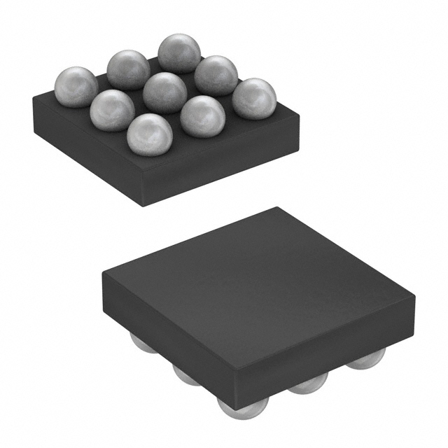
Available in WLCSP1.35x1.35-9 Package
APPLICATIONS
Feature Phone and Smart Phones
Tablets
GPS Receivers
2.5ms shuts down the
IC.
C2
VIN
Power supply input pin. Connect a ceramic capacitor nearby this pin to bypass the IC.
C3
SW
Drain connection of the internal N-CH power MOSFET.
MP3312 Rev. 1.1
12/7/2020
LED2 current sink pin.
LED1 current sink pin.
PWM signal input pin. 5kHz to 100kHz PWM Signal is recommended to this pin to do the
analog current dimming. Low logic for >20ms shuts down the IC.
Internal error amplifier output pin. Connect a capacitor to compensate the system.
GND pin.
www.MonolithicPower.com
MPS Proprietary Information. Patent Protected. Unauthorized Photocopy and Duplication Prohibited.
© 2020 MPS. All Rights Reserved.
7
�MP3312 - 2.7V-5.5V INPUT, 38V OVP, DUAL-CHANNEL WHITE LED DRIVER
FUNCTIONAL BLOCK DIAGRAM
L1
D1
VOUT
VIN
C2
C1
SW
VIN
OVP
Shutdown
OSC
PWM
Control
EN
EN
Detection
PWM
RAMP
Analog
Dimming
VREF
EA
PWM
Comparator
LED1
COMP
Feedback
Control
Min.
Max.
R2
C3
GND
Short
Protection
Current Control
LED2
ISET
EN
R1
Figure 1— Functional Block Diagram
MP3312 Rev. 1.1
12/7/2020
www.MonolithicPower.com
MPS Proprietary Information. Patent Protected. Unauthorized Photocopy and Duplication Prohibited.
© 2020 MPS. All Rights Reserved.
8
�MP3312 - 2.7V-5.5V INPUT, 38V OVP, DUAL-CHANNEL WHITE LED DRIVER
OPERATION
The MP3312 employs the fixed switching
frequency, peak current mode control
architecture and 2 regulated current sinks to
power the LED array. The operation of the
MP3312 can be understood by referring to the
below function block diagram.
System Startup
Either pulling EN or PWM to high enables the
IC operation while pulling EN to GND
for >2.5ms or pulling PWM to GND for >20ms
shuts down the IC.
When enabled, the MP3312 checks the
topology connection first. The MP3312 also
checks other safety limits, including UVLO and
over-temperature protection (OTP). If all the
protections pass, the chip then starts boosting
the step-up converter with an internal soft-start.
It is recommended that the enable signal occurs
after the establishment of the input voltage and
PWM dimming signal during the start-up
sequence to avoid large inrush current.
Switching Operation
At the start of each oscillator cycle the main low
side FET (M1) is turned on through the control
circuitry. To prevent sub-harmonic oscillation at
duty cycle greater than 50 percent, a stabilizing
ramp is added to the output of the current
sense amplifier and the result is fed into the
positive input of the PWM generation
comparator. When this voltage equals the
output voltage of the error amplifier the main
power FET is turned off. Then the inductor
current flows through the free-wheeling diode,
which forces the inductor current to decrease.
The output voltage of the internal error amplifier
is an amplified signal of the difference between
the reference voltage and the feedback voltage.
The converter automatically chooses the lowest
active LEDX pin voltage to provide a highenough bus voltage to power all the LED arrays.
If the feedback voltage drops below the
reference, the output of the error amplifier
increases. It results in more current flowing
through the MOSFET, thus increasing the
MP3312 Rev. 1.1
12/7/2020
power delivered to the output. This forms a
closed loop that regulates the output voltage.
Dimming Control
MP3312 supports analog dimming and 1-wire
digital set dimming mode to regulate the WLED
current.
To do analog dimming, apply a PWM signal to
PWM pin by adjusting the LED current
amplitude. The internal filter is integrated and
the PWM signal with 5k~100kHz range is
supported. Internal dimming signal duty
detection circuit automatically changes the
internal reference lineally to regulate the current.
In addition, the EN pin supports 1-wire interface
to do current dimming control. The 1-wire
description and protocol details are as follow.
1-wire Interface
1-wire interface is based on master-slave
structure which is designed for digital dimming.
The EN pin is multipurpose as single port to
receive LED brightness data. The rate to detect
the bit can automatically range from
1.39kBit/sec to 50kBit/sec.
The command sent to chip (slave) contains 24
bits, 9-bit dimming data, 8-bit device address
and RFA bit are included. Chip detects the bit in
series and it transmits the LSB first and MSB
finally.
The control bits description is as below and
Figure 2 shows the command bytes structure in
detail.
D0-D8 are the dimming data bits which
achieve 9-bit dimming resolution
Bit9 and bit11-bit15 is reserved. Set to 0
RFA bit indicates master needs Request of
Acknowledge or not.
Device address byte is DA0-DA7. The
device address byte is set to 0x8F.
www.MonolithicPower.com
MPS Proprietary Information. Patent Protected. Unauthorized Photocopy and Duplication Prohibited.
© 2020 MPS. All Rights Reserved.
9
�MP3312 - 2.7V-5.5V INPUT, 38V OVP, DUAL-CHANNEL WHITE LED DRIVER
Address Byte
Data Byte
Data in
Start
D0
D1
D2
D3
D4
D5
D6
D7
D8
Bit9
0
RFA
bit11-bit15
(00000)
MSB
DA0 DA1 DA2 DA3 DA4 DA5 DA6 DA7
1
1
1
1
0
0
0
1
E0S
LSB
Figure 2—1-wire command structure
1-wire interface defines logic 0 and logic 1 by
comparing the time of the signal low level and
high level, 1 cycle means 1 logic bit. The bit
detection starts with a falling edge on the EN
pin and ends with the next falling edge. Shown
as Figure 3
Low logic (logic 0): tLOW≥3* tHIGH
1. Pulling VIN and PWM to high.
High logic (logic 1): tHIGH≥3* tLOW
2. Pulling data line from low to high for tDELAY (1wire detection delay time, 100us) and this
rising edge is the start of 1-wire detection
window.
tLOW
tHIGH
tHIGH
tLOW
The EN pin needs to distinguish EN signal and
digital dimming signal when set up boost driver.
Chip only receives 1-wire signal when EN pin
signal matches 1-wire protocol during 1ms 1wire detection window. 1-wire dimming
sequence is described as below, and shown in
Figure 4.
3. After 1-wire detection delay time, pulling data
line to low for more than tDETECTION (1-wire
detection time, 260us). Then pulling data
line to high.
Logic “1”
Logic “0”
Figure 3—1-Wire Bit Definition
4. The sum of 1-wire detection delay time and
1-wire detection time should be less than tWIN.
(The time of 1-wire detection window,1ms).
PWM
Detection
Window
Programming
Code
Programming
Code
Detection
Window
Interval
time
Programming
Code
EN
Detection
Time
Detection
Delay
ILED
Start Up Delay
Ramp
Up
Ramp Up
Shut Down
Delay
Figure 4—1-Wire Dimming Sequence
MP3312 Rev. 1.1
12/7/2020
www.MonolithicPower.com
MPS Proprietary Information. Patent Protected. Unauthorized Photocopy and Duplication Prohibited.
© 2020 MPS. All Rights Reserved.
10
�MP3312 - 2.7V-5.5V INPUT, 38V OVP, DUAL-CHANNEL WHITE LED DRIVER
In addition, before chip starts to receive each
command with first falling edge, data line should
keep high level for tSTART (min. 2us) time. which
The transmission of each command is completed
with low level for tEOS (min. 2us).Shown in Figure
5.
The ACK signal feedback to master or not is
dependent on RFA bit. If ACK is needed, the
master should have an open-drain output, and
data line should be pulled high by master with a
resistor load.
There is a counter (typical: 2MHz/13bits) to
measure the time of the high/low level in 1-Wire
interface. The counter keeps work in the interval
time between 2 commands, and it will recount
after time out in single level. For preventing the
mis-trigger, the counter of the interval time
should result at the value larger than 5, otherwise
the first bit of the next command will be missed. If
bit-missed happens, the bit-malposition will
happen in later communication process, and it
will cause 1-Wire communication fail (1-Wire
digital set dimming fail) since for the wrong
address byte. Increasing the tEOS will do help for
MP3312 to recover from communication failure
(when tEOS=300us, the communication fail will
recover soon)
tSTART
tEOS
Address Bits
Data Bits
Static High
Static High
Data In
D0
D8
Bit9
RFA=0
Bit15
DA0
DA7
Figure 5— Data-line Timing when RFA=0
tSTART
Data In
tACKval
Address Bits
Data Bits
Static High
Static High
D0
D8
Bit9
RFA=1
Bit15
DA0
DA7
tACK
ACK signal is “ture”.
Data line is pulled down by
slave
Data out
(ACK signal is “ true”)
Date line needs be pulled
high by master with
resistor load to detect ACK
signal
Data out
(ACK signal is “false”)
ACK signal is “false”.
Data line is not pulled down
by slave
Figure 6—Data-line Timing when RFA=1
If RFA=0, No ACK signal feedback. After all 24
bits data is transferred, data line keeps low for
MP3312 Rev. 1.1
12/7/2020
www.MonolithicPower.com
MPS Proprietary Information. Patent Protected. Unauthorized Photocopy and Duplication Prohibited.
© 2020 MPS. All Rights Reserved.
11
�MP3312 - 2.7V-5.5V INPUT, 38V OVP, DUAL-CHANNEL WHITE LED DRIVER
tEOS (min. 2us) delay, and then it is pulled to static
high. Shown as Figure 5.
If RFA=1, ACK signal feedback to master. After
all 24 bits data is transferred, the data line keeps
low for tACKval (max. 2us) time ,then data line
should be released to output high impedance and
master is ready to detect the ACK signal from
slave . After tACKval, if ACK “false” (1-wire data is
not received successfully), the data line will be
pulled to high directly. After tACKval, if ACK “ture”
(1-wire data is received successfully), data line
will be continuously pulled to low VACKL (max.
0.4V) by slave for tACK (max. 512us) time. The
master reads this low logic, it means chip
received 1-wire data successfully. Then the data
line is pulled to static high. Shown as Figure 6.
MP3312 has a 9-bit DAC for digital dimming
control and the dimming resolution is 1/511. The
default code value of D0 (LSB)-D8(MSB) is
“111111111” when the device is first enabled.
The LED current is dependent on the internal
register value D0-D8 according to below formula:
ILED ILEDfull
Unused LED Channel
In some cases, if one LED current channel is not
used, connect the corresponding LEDx to GND
to remove it from the control loop.
Short String Protection
The MP3312 monitors the LEDX pin voltage to
judge if the short string occurs. If one string is
short, the respective LEDX pin will be pulled up
to the boost output and tolerate high voltage
stress. If the LEDX pin voltage is higher than 5 V
and LED current is larger than 8% full-scale
setting current, the short string condition is
detected and if such condition lasts longer than
8ms, the fault string current source is disabled till
VIN and EN is reset for enable again.
Thermal Shutdown Protection
To prevent the IC operate at exceedingly high
temperature, thermal shutdown is implemented in
this chip by detecting the silicon die temperature.
When the die temperature exceeds the upper
threshold 150℃, the IC shutdowns and recovers
to normal operation when die temperature drops
below lower threshold. Typically, the hysteresis
value is 25°C.
code
511
ILEDfull is the full scale output current set by RISET
to ISET pin. Code is the DEC value of resolution
bit (D0-D8).
Cycle-by-Cycle Current Limit Protection
MP3312 provides cycle-by-cycle current limit
protection to avoid any damage due to too large
current rating. During startup, the current limit is
clamped to 1A for around 6ms to avoid output
overshoot and inrush current. After that, the
current limit returns back to normal 1.8A.
Open String Protection
Open string protection is achieved by detecting
the VOUT pin. If the LED string is open, the
feedback voltage is lower than the reference
voltage, thus the COMP rises up and keeps
charge the output capacitor until VOUT pin hits
the protection point VOVP. Then the IC stops
switching and shuts down till VIN and EN is reset
for enable again.
MP3312 Rev. 1.1
12/7/2020
www.MonolithicPower.com
MPS Proprietary Information. Patent Protected. Unauthorized Photocopy and Duplication Prohibited.
© 2020 MPS. All Rights Reserved.
12
�MP3312 - 2.7V-5.5V INPUT, 38V OVP, DUAL-CHANNEL WHITE LED DRIVER
APPLICATION INFORMATION
Setting the LED Current
The full scale LED current can be set through the
current setting resistor on the FB pin.
ILED(mA)
VISET (V)
* 1020
RISET (k)
For VISET=1.232V, RISET=63.4kΩ, the LED current
is set to 20mA. Please do not leave ISET pin
open.
Selecting the Input Capacitor
The input capacitor reduces the surge current
drawn from the input supply and the switching
noise from the device. The input capacitor
impedance at the switching frequency should be
much less than the input source impedance to
prevent the high-frequency switching current
from passing through to the input. Use ceramic
capacitors with X5R or X7R dielectrics for their
low ESR and small temperature coefficients. For
most applications, a 1uF~4.7μF ceramic
capacitor is ok.
Selecting the Inductor
The MP3312 requires an inductor to supply a
higher output voltage while being driven by the
input voltage. A larger value inductor results in
less ripple current, resulting in lower peak
inductor current and reducing stress on the
internal N-channel MOSFET. However, the larger
value inductor has a larger physical size, higher
series resistance, and lower saturation current.
Choose an inductor that does not saturate under
the worst-case load conditions. Select the
minimum inductor value to ensure that the boost
converter works in continuous conduction mode
with high efficiency and good EMI performance.
Calculate the required inductance value using the
equation:
η VOUT D (1 D)
2 fSW ILOAD
2
L
D 1
VIN
VOUT
Where VIN and VOUT are the input and output
voltages, fSW is the switching frequency, ILOAD is
the total LED load current, and η is the efficiency.
The switching current is used for the peak current
MP3312 Rev. 1.1
12/7/2020
mode control. In order to avoid hitting the current
limit, the worst-case inductor peak current should
be less than 80% of the current-limit ILIM.
Generally, a 4.7uH~10uH inductor is ok to cover
most of the applications. Note that the system
efficiency is dependent on the DC resistance of
inductor, and larger DC resistance causes larger
power loss.
Selecting the Output Capacitor
The output capacitor keeps the output voltage
ripple small and ensures feedback loop stability.
The output capacitor impedance must be low at
the switching frequency. Ceramic capacitors with
X7R dielectrics are recommended for their low
ESR characteristics. Care must be taken that
ceramic capacitance is also dependent on the
voltage rating; DC bias voltage and the value can
loss as much as 50% of its capacitance at its
rated voltage rating. Please leave enough
voltage rating margin when select the component.
In addition, too low capacitance will cause the
loop instability. For most applications, a
1μF~4.7μF ceramic capacitor is ok.
Selecting the External Schottky Diode
To optimize the efficiency, a high-speed and low
reverse recovery current schottky diode is
recommended. Make sure the diode’s average
and peak current rating exceeds the output
average LED current and the peak inductor
current. In addition, the diode’s break-down
voltage rating should be large than the maximum
voltage across the diode. Usually, unexpected
high frequency spike voltage can be seen across
the diode when the diode turns off. So, leaving
some voltage rating margin is always needed to
guarantee normal long term operation when
selecting a diode.
Layout Considerations
Careful attention must be paid to the PCB board
layout and components placement. Proper layout
of the high frequency switching path is critical to
prevent noise and electromagnetic interference
problems. The loop of MP3312’s internal low side
MOSFET, schottky diode, and output capacitor is
flowing with high frequency ripple current, it must
be minimized. So the input and output capacitor
should be placed to IC as close as possible.
www.MonolithicPower.com
MPS Proprietary Information. Patent Protected. Unauthorized Photocopy and Duplication Prohibited.
© 2020 MPS. All Rights Reserved.
13
�MP3312 - 2.7V-5.5V INPUT, 38V OVP, DUAL-CHANNEL WHITE LED DRIVER
TYPICAL APPLICATION CIRCUITS
L1
VIN
GND
D1
4.7uH
C2
1uF
C1
1uF
SW
IN
EN
PWM
EN
MP3312
PWM
LED1
LED2
COMP
ISET
C3
330nF
GND
R1
63.4k
Figure 7— Typical Application for dual string 6LEDs, 20mA/string
MP3312 Rev. 1.1
12/7/2020
www.MonolithicPower.com
MPS Proprietary Information. Patent Protected. Unauthorized Photocopy and Duplication Prohibited.
© 2020 MPS. All Rights Reserved.
14
�MP3312 - 2.7V-5.5V INPUT, 38V OVP, DUAL-CHANNEL WHITE LED DRIVER
PACKAGE INFORMATION
WLCSP1.35X1.35-9
PIN 1 ID
PIN 1 ID
MARKING
PIN 1 ID INDEX
AREA
BOTTOM VIEW
TOP VIEW
SIDE VIEW
NOTE:
1) ALL DIMENSIONS ARE IN MILLIMETERS.
2) BALL COPLANARITY SHALL BE 0.05
MILLIMETER MAX.
3) JEDEC REFERENCE IS MO-211,
VARIATION BC.
4) DRAWING IS NOT TO SCALE.
RECOMMENDED LAND PATTERN
MP3312 Rev. 1.1
12/7/2020
www.MonolithicPower.com
MPS Proprietary Information. Patent Protected. Unauthorized Photocopy and Duplication Prohibited.
© 2020 MPS. All Rights Reserved.
15
�MP3312 - 2.7V-5.5V INPUT, 38V OVP, DUAL-CHANNEL WHITE LED DRIVER
Revision History
Revision #
Revision date
1.1
12/7/2020
Description
add the explanation on the failure issue of 1-wire
communication
Pages
Updated
11
NOTICE: The information in this document is subject to change without notice. Please contact MPS for current specifications.
Users should warrant and guarantee that third party Intellectual Property rights are not infringed upon when integrating MPS
products into any application. MPS will not assume any legal responsibility for any said applications.
MP3312 Rev. 1.1
12/7/2020
www.MonolithicPower.com
MPS Proprietary Information. Patent Protected. Unauthorized Photocopy and Duplication Prohibited.
© 2020 MPS. All Rights Reserved.
16
�


 工商网监
湘ICP备2023018690号
工商网监
湘ICP备2023018690号
