MP3331
2A, Synchronous Boost Flash LED Driver
with I2C Interface
The Future of Analog IC Technology
DESCRIPTION
FEATURES
The MP3331 is a highly-efficient, 2A, single flash
LED driver in a very compact package for highresolution camera phones that improves image and
video quality in low-light environments. The device
operates in a 1/2/3/4MHz synchronous DC/DC
boost converter to provide an optimized solution for
smaller PCB spaces with higher efficiency.
The MP3331 features a standard I2C interface,
single LED channel, rich protection modes, and
high power density and performances. It supports
flash/assist/torch/indicator/5V DC modes.
The cathode of the flash LED is referenced to GND,
which improves thermal performance. It is available
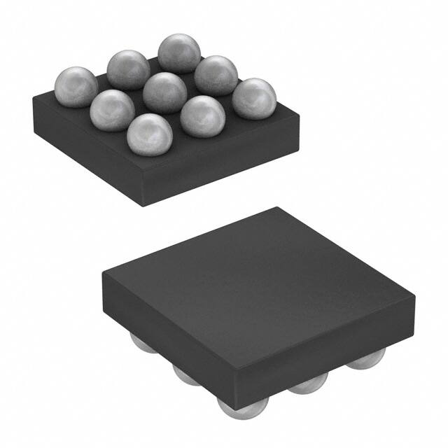
in a WLCSP9-1.7mm x 1.7mm package.
2.7V to 5.5V Input Voltage
1/2/3/4MHz Selectable Switching Frequency
Switching Frequency Foldback Function
400kHz I2C Compatible Interface
Standby/Flash/Assist/Torch/Indicator/5V DC
Mode
FLASH MODE:
Up to 2A Programmable Current with
+/-7% Accuracy
ASSIST/TORCH MODE:
Up to 508mA Programmable Current with
+/-7% Accuracy
INDICATOR MODE:
Works in 31.5kHz PWM Dimming Mode with
2/16, 3/16, 4/16, 5/16 Duty Cycle
5V DC MODE:
Fixed 5V Output Voltage
External Torch/Strobe Pin
Low-Battery Voltage Protection
Pre-Flash for Auto Detect Load Condition
LED Short/Open Protection
VOUT-GND Short Protection
Over-Voltage Protection
Over-Temperature Protection
Input Under-Voltage Lockout Protection
Thermal Protection
Input to Output Disconnection Function
Available in a WLCSP9-1.7mm x 1.7mm
Package
APPLICATIONS
Camera Phone LED Flash
Tablets
Digital Still Camera
All MPS parts are lead-free, halogen-free, and adhere to the RoHS directive.
For MPS green status, please visit the MPS website under Quality Assurance.
“MPS” and “The Future of Analog IC Technology” are registered Ttademarks of
Monolithic Power Systems, Inc.
MP3331 Rev. 1.04
5/22/2019
www.MonolithicPower.com
MPS Proprietary Information. Patent Protected. Unauthorized Photocopy and Duplication Prohibited.
© 2019 MPS. All Rights Reserved.
1
�MP3331-2A SYNCHRONOUS BOOST FLASH LED DRIVER WITH I2C INTERFACE
TYPICAL APPLICATION
Typical Application Circuit
MP3331 Rev. 1.04
5/22/2019
www.MonolithicPower.com
MPS Proprietary Information. Patent Protected. Unauthorized Photocopy and Duplication Prohibited.
© 2019 MPS. All Rights Reserved.
2
�MP3331-2A SYNCHRONOUS BOOST FLASH LED DRIVER WITH I2C INTERFACE
ORDERING INFORMATION
Part Number*
MP3331GC
Package
WLCSP-9 (1.7mm x 1.7mm)
Top Marking
See Below
* For Tape & Reel, add suffix –Z (e.g. MP3331GC)
TOP MARKING
CM: Product code of MP3331GC
Y: Year code
LLL: Lot number
PACKAGE REFERENCE
WLCSP-9 (1.7mm x 1.7mm)
MP3331 Rev. 1.04
5/22/2019
www.MonolithicPower.com
MPS Proprietary Information. Patent Protected. Unauthorized Photocopy and Duplication Prohibited.
© 2019 MPS. All Rights Reserved.
3
�MP3331-2A SYNCHRONOUS BOOST FLASH LED DRIVER WITH I2C INTERFACE
ABSOLUTE MAXIMUM RATINGS (1)
All the pins....................................... -0.3V to +6V
Junction temperature ................................ 150°C
Lead temperature...................................... 260°C
Continuous power dissipation (TA = 25°C) (2)
WLCSP-9 (1.7mm x 1.7mm) .................... 1.14W
Recommended Operating Conditions (3)
Supply voltage (VIN) ........................ 2.7V to 5.5V
Operating junction temp............-40°C to +125°C
MP3331 Rev. 1.04
5/22/2019
Thermal Resistance (4)
θJA
θJC
WLCSP-9 (1.7mm x 1.7mm)….110….0.5..°C/W
NOTES:
1) Exceeding these ratings may damage the device.
2) The maximum allowable power dissipation is a function of the
maximum junction temperature TJ (MAX), the junction-toambient thermal resistance θJA, and the ambient temperature
TA. The maximum allowable continuous power dissipation at
any ambient temperature is calculated by PD (MAX) = (TJ
(MAX)-TA)/θJA. Exceeding the maximum allowable power
dissipation will produce an excessive die temperature,
causing the regulator to go into thermal shutdown. Internal
thermal shutdown circuitry protects the device from
permanent damage.
3) The device is not guaranteed to function outside of its
operating conditions.
4) Measured on JESD51-7, 4-layer PCB.
www.MonolithicPower.com
MPS Proprietary Information. Patent Protected. Unauthorized Photocopy and Duplication Prohibited.
© 2019 MPS. All Rights Reserved.
4
�MP3331-2A SYNCHRONOUS BOOST FLASH LED DRIVER WITH I2C INTERFACE
ELECTRICAL CHARACTERISTICS
VIN = 3.6V, TA = 25°C, unless otherwise noted.
Parameters
Symbol
Condition
Min
Typ
Max
Units
5.5
V
Supply
Operating input voltage
Input UVLO threshold
VIN
VIN_UVLO
2.7
Rising edge
Input UVLO hysteresis
Standby current
Operating quiescent current
IQ_STANDBY
IQ
VIN = 2.7V to 5.5V,
active
VIN = 3.6V, No switching, pass
mode
2.5
V
150
mV
I2C
10
0.95
μA
mA
Switching Regulator
Switching frequency
Minimum on time
fs
Fs = 4MHz
3.6
tON_MIN
4
4.4
MHz
50
ns
NMOS on resistance
RDSON_N
VIN = 3.6V
80
mΩ
PMOS on resistance
RDSON_P
VIN = 3.6V
120
mΩ
Constant DC output voltage
VOUT_5V
5V DC mode
Code setting = 00, max duty
cycle(5)
Code setting = 11, max duty
cycle(5)
5
V
1.9
A
4.2
A
0
mA
Inductor current limit
ILIMIT
LED Driver
Flash current setting
Torch current setting
Current source headroom
voltage
Current ramp-up step time
Current ramp-down step
time
Flash to TX current settling
time
Digital Input
ILED_FLASH
ILED_TORCH
VHD
tRAMP_UP
Flash mode,
value setting = 000000
Flash mode,
value setting = 001010
Assist light/torch mode,
value setting = 000000
Assist light /torch mode,
value setting = 001010
Current = 200mA
Current =
295
295
1500mA(5)
TUP_I = 000
317
MP3331 Rev. 1.04
5/22/2019
mA
mA
339
mA
150
mV
250
mV
8
μs
2
μs
TX from low to high, ILED from
1500mA to 31.7mA
Input logic-low voltage
Input logic-high Voltage
339
0
tRAMP_DOWN
tSETTLE
317
1.2
www.MonolithicPower.com
MPS Proprietary Information. Patent Protected. Unauthorized Photocopy and Duplication Prohibited.
© 2019 MPS. All Rights Reserved.
5
μs
0.4
V
V
5
�MP3331-2A SYNCHRONOUS BOOST FLASH LED DRIVER WITH I2C INTERFACE
ELECTRICAL CHARACTERISTICS (continued)
VIN = 3.6V, TA = 25°C, unless otherwise noted.
Parameters
Strobe/Torch/TX pull-down
resistor
Protection
Symbol
Time-out time
tTIMEOUT
Over-voltage threshold
Condition
Min
Typ
Max
250
Time setting code = 0011
VOVP
LED short detection voltage
VLED_ST
VOUT short blanking time
TOUT_ST
LED open detection voltage
Thermal shutdown threshold(5)
Adaptive thermal threshold(5)
VLED_OP
Tj_SD
Low-battery threshold
VBAT_LOW
VOUT130 C
VSW
2V/div.
VOUT
5V/div.
IL
1A/div.
ILED
500mA/div.
MP3331 Rev. 1.04
5/22/2019
www.MonolithicPower.com
MPS Proprietary Information. Patent Protected. Unauthorized Photocopy and Duplication Prohibited.
© 2019 MPS. All Rights Reserved.
9
�MP3331-2A SYNCHRONOUS BOOST FLASH LED DRIVER WITH I2C INTERFACE
PIN FUNCTIONS
Pin #
Name
A1
OUT
Boost converter output.
A2
SW
Boost converter switching node.
A3
B1
GND
LED
B2
STR
B3
IN
C1
TOR/TX
C2
C3
SDA
SCL
MP3331 Rev. 1.04
5/22/2019
Description
Ground.
Current source for LED. Connect the anode of LED to LED.
Strobe signal input STR synchronizes the flash pulse to the image capture. If STR is
floated, internally pull STR to low weakly.
Input supply. IN provides the power for the internal power and logic circuit. IN must be
bypassed locally.
Torch signal input or synchronization input signal for RF transmission signal. If
TOR/TX is floated, internally pull TOR/TX to low weakly.
I2C interface clock data input.
I2C interface clock signal.
www.MonolithicPower.com
MPS Proprietary Information. Patent Protected. Unauthorized Photocopy and Duplication Prohibited.
© 2019 MPS. All Rights Reserved.
10
�MP3331-2A SYNCHRONOUS BOOST FLASH LED DRIVER WITH I2C INTERFACE
FUNCTIONAL BLOCK DIAGRAM
Figure 2: MP3331 Functional Block Diagram
MP3331 Rev. 1.04
5/22/2019
www.MonolithicPower.com
MPS Proprietary Information. Patent Protected. Unauthorized Photocopy and Duplication Prohibited.
© 2019 MPS. All Rights Reserved.
11
�MP3331-2A SYNCHRONOUS BOOST FLASH LED DRIVER WITH I2C INTERFACE
OPERATION
The MP3331 is a single-channel flash LED driver
with an I2C interface for a camera flash that
supports good image capture. It works in flash
mode, assist mode, torch mode, indicator mode,
and fixed 5V DC output mode.
LED Driver Operation
The MP3331 uses PWM mode with peak
current control to regulate the LED current. It
works in a selectable 1M/2M/3M/4MHz
switching frequency with a synchronous rectifier
PMOS. When enabled, the synchronous PMOS
works as a 350mA current source to charge the
output capacitor until VOUT rises above the 2.3V.
The device will change to boost switching mode
if the voltage across the current source is less
than the target reference. If VIN is very close to
VOUT, the IC works in boost switching mode and
pass mode automatically to minimize the power
loss. In pass mode, the synchronous PMOS is
turned on completely. During the current startup, the current ramps up smoothly step by step
until the target setting current is reached.
Table 1: Mode Configuration
Configuration
TX/TOR
High
X
X
X
X
High
X
X
STR
X
X
X
High
X
High
High
X
LED_EN
1
1
1
1
1
1
1
X
STR_MOD
0
X
X
1
0
1
1
X
Mode
5V_MOD
X
X
X
X
X
X
X
1
LED_MOD
00
10
01
11
11
00
10
X
Torch
Assist light
Indicator
Flash
Flash
Torch to flash
Assist to flash
5V
Standby Mode
In default, if VIN is higher than UVLO, the device
changes to standby mode. The I2C is active and
is ready to communicate with the host. Table 1
shows all work modes for MP3331.
Torch Mode
In standby mode, if TOR goes from low to high
(TX/TOR = 1), the device switches to torch
mode, and the current ramps up step by step
after setting LED_EN to 1. The current for LED
is set through register I_TOR. The ramping up
slew rate is set by register TUP_I. The current
is disabled by pulling TOR to low or by setting
LED_EN bits to 0. By pulling TOR to low,
LED_EN and LED_MOD bits will reset
automatically to default if LED_SD is 0 (see
Figure 3).
MP3331 Rev. 1.04
5/22/2019
Figure 3: Torch Mode
Assist Mode
To enter assist mode, set LED_MOD register to
10 and LED_EN to 1. The current ramps up to
the target value, which is set by I_TOR. The
ramping up slew rate is set by register TUP_I.
The current is disabled by switching to standby
mode or by setting LED_EN bits to 0 (see
Figure 4).
www.MonolithicPower.com
MPS Proprietary Information. Patent Protected. Unauthorized Photocopy and Duplication Prohibited.
© 2019 MPS. All Rights Reserved.
12
�MP3331-2A SYNCHRONOUS BOOST FLASH LED DRIVER WITH I2C INTERFACE
LED_MOD and LED_EN are reset to the default
value, and the time-out fault bit FT_TO is set to
1 and is not cleared until read back or input
power reset (see Figure 6).
Figure 4: Assist Mode
Indicator Mode
The device enters indicator mode, which
provides a low current output when LED_MOD
is set to 01, and LED_EN is set to 1. In this
mode, the driver current sources the output
current in 31.5kHz PWM mode. The current
amplitude is set by I_TOR while the duty cycle
is set by the INDI_PWM register. When
disabled, switch to standby mode or set
LED _EN bits to 0 (see Figure 5).
Figure 5: Indicator Mode
Flash Mode
The device works in flash mode in the following
ways:
Figure 6: Hardware and Level Sensitive Mode
1. Hardware and level sensitive mode.
2. Hardware and edge sensitive mode.
In this mode, STR_MOD = 1, STR_LV = 1,
LED_EN = 1, and LED_MOD = 11. The flash
current starts ramping up after STR goes high.
The current is set by I_FL, and the ramping up
time is set by TUP_I. The flash current ends
when STR is pulled to low. If LED_SD = 0, the
LED_MOD is reset to standby mode, and
LED_EN is set to 0 after the flash. If
LED_SD = 1, the LED_MOD, and LED_EN are
not reset. If the flash timer set by FL_TIM ends
before STR goes low, the flash current
terminates immediately.
In this mode, STR_MOD = 1, STR_LV = 0,
LED_EN = 1, and LED_MOD = 11. The flash
current starts ramping up after STR goes high.
The current is set by I_FL, and the ramping up
time is set by TUP_I. The flash current ends
when the flash timer set by FL_TIM ends. If
LED_SD = 0, the LED_MOD is reset to standby
mode, and LED_EN is set to 0 after the flash. If
LED_SD = 1, the LED_MOD, and LED_EN are
not reset (see Figure 7).
MP3331 Rev. 1.04
5/22/2019
www.MonolithicPower.com
MPS Proprietary Information. Patent Protected. Unauthorized Photocopy and Duplication Prohibited.
© 2019 MPS. All Rights Reserved.
13
�MP3331-2A SYNCHRONOUS BOOST FLASH LED DRIVER WITH I2C INTERFACE
Figure 9: Torch Mode to Flash Mode
Figure 7: Hardware and Edge Sensitive Mode
3. Software and edge sensitive mode
In this mode, STR_MOD = 0, LED_EN = 1, and
LED_MOD = 11. The current is set by I_FL, and
the ramping up time is set by TUP_I. The flash
current ends when the flash timer set by
FL_TIM ends. If LED_SD = 0, the LED_MOD is
reset to standby mode, and LED_EN is set to 0
after the flash. If LED_SD = 1, the LED_MOD,
and LED_EN are not reset (see Figure 8).
Assist Mode to Flash Mode
During assist-light mode, the device can
change to flash mode from assist-light mode
directly when STR goes from low to high (if
STR_MOD = 1). After the flash, the operation is
the same as described in the “Flash Mode”
section (see Figure 10).
Figure 10: Assist Mode to Flash Mode
5V DC Output Mode
Figure 8: Software and Edge Sensitive Mode
Torch Mode to Flash Mode
During torch mode, the device can change to
flash mode from torch mode directly when STR
goes from low to high (if STR_MOD = 1). After
the flash, the operation is the same as
described in the “Flash Mode” section (see
Figure 9).
MP3331 Rev. 1.04
5/22/2019
If 5V_MOD is set to 1, the device works in a
fixed 5V DC output mode, and the control loop
is taken over by the voltage loop. Note that the
LED current sources can still output current if
the mode conditions are met (as described
above). Care must be taken to ensure thermal
temperatures are ok because the 5V powers
the LED directly. To avoid this, it is
recommended to set LED_EN to 0 during the
5V DC mode (see Figure 11).
www.MonolithicPower.com
MPS Proprietary Information. Patent Protected. Unauthorized Photocopy and Duplication Prohibited.
© 2019 MPS. All Rights Reserved.
14
�MP3331-2A SYNCHRONOUS BOOST FLASH LED DRIVER WITH I2C INTERFACE
Figure 11: 5V DC Mode
Switching Frequency Setting
The switching frequency is selected by SW_FS
bits. 1M/2M/3M/4MHz are available to optimize
efficiency.
Switching Frequency Foldback
In default 4MHz switching mode, if the voltage
across the current source is larger than the
value set by the register bits VTH_PAS, the IC
switches to 1MHz mode to improve efficiency
and EMI. In 1MHz mode, the switching
frequency can be stretched down according to
the load condition with FS_SD =0. The IC goes
into pass mode (which turns on the
synchronous PMOS fully) if the input voltage is
high enough.
Current Reduction
When the MP3331 works in flash mode, output
current reduction may occur due to the
following conditions:
1. TX is high.
During flash mode, if TOR/TX goes from low to
high, the flash current drops to the current set
by I_TX in less than 5µs and sets the FT_TX bit
to 1. If TX goes low, the current ramps up to the
flash current again (see Figure 12).
MP3331 Rev. 1.04
5/22/2019
Figure 12: Flash Mode when TX is Active
2. Low battery
triggered.
voltage
threshold
is
During a flash pulse, if the battery voltage drops
below the threshold set by VBL_RUN, the
current reduces step-by-step with a 2µs/step
until the battery voltage rises up to the specific
low battery voltage threshold. Actual current in
the IFL_ACT register can be read back. The
minimum current caused by the current
reduction in IFL_MIN can be read back after the
flash.
Low Battery Voltage Protection
The device provides low battery voltage
protection in flash mode in the following ways:
1. Before the flash, if the input voltage is lower
than the threshold set by VBL_RUN, the device
remains disabled (if VBL_SD = 1 and sets the
fault bit FT_VBATL to 1). If VBL_SD = 0, the
device ramps to the current set by I_TX and
sets the fault bit FT_VBATL to 1. The fault bit is
cleared after read back or the input power
resets.
2. During flash start-up, if the input voltage is
lower than the threshold set by VBL_RUN, the
current stops ramping. The fault bit FT_VBATL
is set. During the flash pulse, if the input voltage
is lower than the threshold set by VBL_RUN,
the current ramps down step-by-step. The fault
bit is set until read back or the input power
resets. After the flash, the minimum current
caused by the current reduction is read back
through the IFL_MIN register. The IFL_MIN
value holds until the next flash occurs or the
power resets. The actual current is read back
through IFL_ACT during flash time. This
www.MonolithicPower.com
MPS Proprietary Information. Patent Protected. Unauthorized Photocopy and Duplication Prohibited.
© 2019 MPS. All Rights Reserved.
15
�MP3331-2A SYNCHRONOUS BOOST FLASH LED DRIVER WITH I2C INTERFACE
function tells the device how much flash current
can be drawn from the battery for the next flash.
Thus, it is possible to do a pre-flash function and
provide continuous stable flash current according
to IFL_MIN information (see Figure 13).
Junction Over-Temperature Protection
If Tj > 130℃, the flash current drops to the
current set by I_TX (if LED_OTAD = 1). The fault
bit FT_OTP is set. If Tj > 150℃, the device stops
switching and resets the mode setting. The fault
bit FT_OTP has to be cleared to 0 by read back
or power reset before the IC will re-start.
Time-Out Protection
If the device works in flash mode with hardware
and level sensitive enabled, the time-out
protection triggers when the STR high-level pulse
is longer than the timer set by FL_TIM. The
device stops switching and resets the mode
setting. The fault bit is 1 until read back or power
reset before the IC re-starts.
UVLO Protection
Figure 13: Pre-Flash Operation
VOUT-GND Short Protection
If VOUT 25mA, the IC marks off
the current source and resets the mode setting
bits. Then the fault bit FT_LEDSC is set. The
fault bit FT_LEDSC is 1 until read back or power
reset.
LED Open Protection
If the VIN drops below the UVLO threshold, the
device stops, and all the registers are reset to
default.
I2C Interface Register Description
I2C Chip Address
After the start condition, the I2C compatible
master sends a 7-bit address followed by an
eighth read (read: 1) or write (write: 0) bit. The
following bit indicates the register address
to/from which the data will be written/read (see
Figure 14 and the Tables below).
Figure 14: I2C Compatible Device Address
If VOUT - VLED < 90mV & VOUT > 5.5V, the IC
stops switching and resets the mode setting bits.
Then the fault bits FT_OVP and FT_LEDOP are
set. The fault bits FT_OVP and FT_LEDOP are 1
until read back or power reset.
Output Over-Voltage Protection
If VOUT > 5.5V, the device stops switching and
resumes normal operation until VOUT drops
below 5.2V. The fault bit FT_OVP is 1 until read
back or power reset.
MP3331 Rev. 1.04
5/22/2019
www.MonolithicPower.com
MPS Proprietary Information. Patent Protected. Unauthorized Photocopy and Duplication Prohibited.
© 2019 MPS. All Rights Reserved.
16
�MP3331-2A SYNCHRONOUS BOOST FLASH LED DRIVER WITH I2C INTERFACE
Register Mapping:
Add
D7
D6
D5
D4
D3
D2
D1
D0
00H
DEV_ID4
DEV_ID3
DEV_ID2
DEV_ID1
DEV_ID0
REV_ID2
REV_ID1
REV_ID0
01H
STR_LV
STR_MOD
STR_POL
LED_EN
TX_TOR
LED_MOD1
LED_MOD0
5V_MOD
02H
NA
NA
NA
IL_PEAK1
IL_PEAK0
FS_SD
NA
NA
03H
FL_TIM3
FL_TIM2
FL_TIM1
FL_TIM0
LED_SD
NA
SW_FS1
SW_FS0
04H
VBL_RUN2
VBL_RUN1
VBL_RUN0
VBL_SD
NA
NA
NA
NA
05H
LED_OTA
D
TUP_I2
TUP_I1
TUP_I0
VTH_PAS1
VTH_PAS0
INDI_PWM1
INDI_PWM0
06H
NA
NA
I_FL5
I_FL4
I_FL3
I_FL2
I_FL1
I_FL0
07H
NA
NA
I_TX5
I_TX4
I_TX3
I_TX2
I_TX1
I_TX0
08H
NA
NA
IFL_ACT5
IFL_ACT4
IFL_ACT3
IFL_ACT2
IFL_ACT1
IFL_ACT0
09H
NA
NA
IFL_MIN5
IFL_MIN4
IFL_MIN3
IFL_MIN2
IFL_MIN1
IFL_MIN0
0AH
NA
NA
I_TOR5
I_TOR4
I_TOR3
I_TOR2
I_TOR1
I_TOR0
0BH
FT_VBATL
FT_OVP
FT_VOSC
FT_LEDSC
FT_OTP
FT_TO
FT_TX
NA
0CH
NA
NA
NA
NA
NA
NA
NA
FT_LEDOP
Table 1: Chip ID Register
Addr: 0x00
Bit
Bit Name
Access
Default
2:0
REV_ID
R
000
7:3
DEV_ID
R
00011
MP3331 Rev. 1.04
5/22/2019
Description
Revision ID
Device ID
www.MonolithicPower.com
MPS Proprietary Information. Patent Protected. Unauthorized Photocopy and Duplication Prohibited.
© 2019 MPS. All Rights Reserved.
17
�MP3331-2A SYNCHRONOUS BOOST FLASH LED DRIVER WITH I2C INTERFACE
Table 2: Mode Setting Register
Addr: 0x01
Bit
Bit Name
Access
Default
Description
7
STR_LV
RW
1
Flash mode trigger mode with STR signal.
0 = edge sensitive; 1 = level sensitive.
6
STR_MOD
RW
1
STR enable bit.
0 = software enable; 1 = hardware enable.
5
STR_POL
RW
1
STR signal input active polarity.
0 = active low; 1 = active high.
4
LED_EN
RW
0
LED current source enable bit.
0 = LED current sink disable; 1 = enable
3
TX_TOR
RW
0
TX mode or torch mode selection bit;
0 indicates TX/TOR used for TX signal;
1 indicates TX/TOR used for torch signal. In flash mode,
TX/TOR is forced to be used as a TX signal pin regardless
of what this bit is.
2:1
LED_MOD
RW
00
Device mode setting bits.
00 = standby/torch mode; 01 = indicator mode;
10 = assist light mode;
11 = flash mode.
0
5V_MOD
RW
0
5V DC output enable bit.
0 = disable; 1 = enable.
Table 3: Peak Current Setting Register
Addr: 0x02
Bit
Bit Name
Access
Default
7:5
NA
RW
000
Reserved.
4:3
IL_PEAK
RW
01
Inductor current limit setting bits.
00 = 1.9A, 01 = 2.8A,10 = 3.6A,11 = 4.2A
Disable switching frequency stretching down from 1MHz if
VIN voltage is close to VOUT voltage.
0 = Enable Fs stretching down function.
1 = Disable Fs stretching down function.
2
FS_SD
RW
0
0:1
NA
RW
NA
MP3331 Rev. 1.04
5/22/2019
Description
Reserved.
www.MonolithicPower.com
MPS Proprietary Information. Patent Protected. Unauthorized Photocopy and Duplication Prohibited.
© 2019 MPS. All Rights Reserved.
18
�MP3331-2A SYNCHRONOUS BOOST FLASH LED DRIVER WITH I2C INTERFACE
Table 4: Flash Timer Setting Register
Addr: 0x03
Bit
Bit Name
Access
Default
Description
7:4
FL_TIM
RW
0001
3
LED_SD
RW
0
0 = reset LED_MOD and LED_EN to default value
after flash or torch. 1 = no reset.
2
NA
RW
0
Reserved.
1:0
SW_FS
RW
00
Switching frequency setting bits. 00 = 4MHz;
01 = 3MHz; 10 = 2MHz;11 = 1MHz.
Flash timer setting bits. 50ms to 800ms, 50ms/step.
0000 = 50ms; 0001 = 100ms; …; 1111 = 800ms.
LED_MOD and LED_EN resetting control bit.
Table 5: Low Battery Voltage Setting Register
Addr: 0x04
Bit
7:5
Bit Name
VBL_RUN
Access
RW
Default
Description
111
Low battery voltage setting bits. If VIN drops below
this voltage during start-up, the current ramping
stops. If VIN drops below this voltage during the
flash current pulse, the current is decreased until
VIN is higher than its threshold. It works only in flash
mode. 000 = 3V; 001 = 3.1V; ...110 = 3.6V;
111 = disabled; 0.1V per step.
Device disabled or reduce the flash current selection
bit when VIN is less than the threshold set by
VBL_RUN before the flash.
1 = device disabled;
0 = Enable and the current ramps up to the current
set by I_TX.
4
VBL_SD
RW
1
3:0
NA
RW
NA
MP3331 Rev. 1.04
5/22/2019
www.MonolithicPower.com
MPS Proprietary Information. Patent Protected. Unauthorized Photocopy and Duplication Prohibited.
© 2019 MPS. All Rights Reserved.
NA
19
�MP3331-2A SYNCHRONOUS BOOST FLASH LED DRIVER WITH I2C INTERFACE
Table 6: Indicator Register
Addr: 0x05
Bit
Bit Name
Access
Default
7
LED_OTAD
RW
0
6:4
TUP_I
RW
001
Description
Adaptive thermal flash current control bit.
1 = current reduced to the current set by I_TX when
Tj >130℃; 0 = disable when Tj >150℃.
Current ramp-up time per step.
000 = 8µs;
001 = 16µs; …111 = 64µs/step.
111 reserved.
3:2
VTH_PAS
RW
01
Defines the threshold when Fs drops to 1MHz or
switches to pass mode from boost mode.
00 = 300mV, 01 = 450mV, 10 = 600mV,
11 = 750mV.
1:0
INDI_PWM
RW
00
PWM duty cycle of 31.5kHz in indicator mode.
00 = 2/16; 01 = 3/16; 10 = 4/16; 11 = 5/16.
Table 7: LED Flash Current Setting Register
Addr: 0x06
Bit
Bit Name
Access
Default
7:6
NA
RW
NA
5:0
I_FL
RW
010000
Description
Reserved.
LED flash current setting bits.
0 to 2000mA, 31.7mA/step.
000000 = 0mA; 000001= 31.7mA…111111 =
2000mA. (Default 010101 = 508mA)
Table 8: TX Current Setting Register
Addr: 0x07
Bit
Bit Name
Access
Default
7:6
NA
RW
NA
RW
010000
Description
Reserved.
Defines the flash current in flash mode if TX is
high.
0 to 2000mA, 31.7mA/step.
000000 = 0mA; 000001= 31.7mA…111111 =
2000mA. (Default 010000 = 508mA).
5:0
I_TX
MP3331 Rev. 1.04
5/22/2019
www.MonolithicPower.com
MPS Proprietary Information. Patent Protected. Unauthorized Photocopy and Duplication Prohibited.
© 2019 MPS. All Rights Reserved.
20
�MP3331-2A SYNCHRONOUS BOOST FLASH LED DRIVER WITH I2C INTERFACE
Table 9: Actual Flash LED Current Register
Addr: 0x08
Bit
Bit Name
Access
Default
7:6
NA
R
NA
5:0
IFL_ACT
R
000000
Description
Reserved.
The actual flash current in flash mode. It can be
read only during flash.
0 to 2000mA, 31.7mA/step.
000000 = 0mA; 000001= 31.7mA …111111 =
2000mA.
Table 10: Minimum Flash LED Current Register
Addr: 0x09
Bit
Bit Name
Access
Default
7:6
NA
R
NA
5:0
IFL_MIN
R
000000
Description
Reserved.
The minimum flash current caused by low battery
voltage current reduction in flash mode.
0 to 2000mA, 31.7mA/step.
000000 = 0mA; 000001= 31.7mA … 111111 =
2000mA.
Table 11: LED Torch Current Setting Register
Addr: 0x0A
Bit
Bit Name
Access
Default
7:6
NA
R
NA
5:0
MP3331 Rev. 1.04
5/22/2019
I_TOR
RW
001000
Description
Reserved.
LED torch current setting bits.
0 to 508mA, 31.7mA/step.
000000 = 0mA, 000001= 31.7mA …010000 =
508mA.
(Default 001000 = 254mA)
www.MonolithicPower.com
MPS Proprietary Information. Patent Protected. Unauthorized Photocopy and Duplication Prohibited.
© 2019 MPS. All Rights Reserved.
21
�MP3331-2A SYNCHRONOUS BOOST FLASH LED DRIVER WITH I2C INTERFACE
Table 12: Fault Indication Register
Addr: 0x0B
Bit
Bit Name
Access
Default
7
FT_VBATL
R
0
6
FT_OVP
R
0
5
FT_VOSC
R
0
4
FT_LEDSC
R
0
3
FT_OTP
R
0
2
FT_TO
R
0
1
FT_TX
R
0
0
NA
R
NA
Description
Low battery voltage fault bit.
0 = no fault.
1 = fault.
Output over voltage fault bit.
0 = no fault.
1 = fault.
VOUT-GND short fault bit.
0 = no fault.
1 = fault.
LED short fault bit.
0 = no fault
1 = fault.
Junction over-temperature fault bit.
0 = no fault
1 = fault.
Flash time out fault bit.
0 = no fault.
1 = fault.
TX fault bit.
0 = no fault.
1 = fault.
NA
Table 13: Fault Indication Register
Addr: 0x0C
Bit
Bit Name
Access
Default
7:2
NA
R
NA
Reserved.
1
NA
R
NA
Reserved.
0
FT_LEDOP
R
0
MP3331 Rev. 1.04
5/22/2019
Description
LED open fault bit.
0 = no fault;
1 = fault.
www.MonolithicPower.com
MPS Proprietary Information. Patent Protected. Unauthorized Photocopy and Duplication Prohibited.
© 2019 MPS. All Rights Reserved.
22
�MP3331-2A SYNCHRONOUS BOOST FLASH LED DRIVER WITH I2C INTERFACE
APPLICATION INFORMATION
Selecting the Input Capacitor
The input capacitor reduces the surge current
drawn from the input supply and the switching
noise from the device. The input capacitor
impedance at the switching frequency should be
less than the input source impedance to prevent
the high-frequency switching current from
passing through to the input. Use ceramic
capacitors with X5R or X7R dielectrics for their
low ESR and small temperature coefficients. A
higher value capacitor helps reduce the input
voltage ripple and noise. For most applications, a
10μF ceramic capacitor will suffice.
Selecting the Inductor
The converter requires an inductor to supply a
higher output voltage while being driven by the
input voltage. A larger value inductor results in
less ripple current, resulting in lower peak
inductor current and reducing stress on the
internal N-channel MOSFET. However, the larger
value inductor has a larger physical size, a higher
series resistance, and a lower saturation current.
Choose an inductor that does not saturate under
the worst-case load conditions. Select the
minimum inductor value to ensure that the boost
converter works in continuous conduction mode
(CCM) with high efficiency and good EMI
performance.
Calculate the required inductance value using
Equation (1) and Equation (2):
η VOUT D (1 D)2
L
(1)
2 fSW ILOAD
D 1
MP3331 Rev. 1.04
5/22/2019
VIN
VOUT
Where VIN and VOUT are the input and output
voltages, fSW is the switching frequency; ILOAD is
the LED load current, and η is the efficiency.
The switching current is used for the peak current
mode control. In order to avoid reaching the
current limit, the worst-case inductor peak current
should be less than 80% of the current-limit (ILIM).
For most applications, 0.47uH~2uH inductor will
suffice.
Selecting the Output Capacitor
The output capacitor keeps the output voltage
ripple small and ensures feedback loop stability.
The output capacitor impedance must be low at
the switching frequency. Ceramic capacitors with
X7R dielectrics are recommended for their low
ESR characteristics. Please note that ceramic
capacitance is dependent on the voltage rating; a
DC bias voltage and the value can lose as much
as 50% of its capacitance at its rated voltage
rating. Please leave a large enough voltage
rating margin when selecting the component. In
addition, too low a capacitance value will cause
loop instability. For most applications, a 10μF
ceramic capacitor will suffice.
(2)
www.MonolithicPower.com
MPS Proprietary Information. Patent Protected. Unauthorized Photocopy and Duplication Prohibited.
© 2019 MPS. All Rights Reserved.
23
�MP3331-2A SYNCHRONOUS BOOST FLASH LED DRIVER WITH I2C INTERFACE
TYPICAL APPLICATION CIRCUITS
Figure 15: Typical Application Circuit
MP3331 Rev. 1.04
5/22/2019
www.MonolithicPower.com
MPS Proprietary Information. Patent Protected. Unauthorized Photocopy and Duplication Prohibited.
© 2019 MPS. All Rights Reserved.
24
�MP3331-2A SYNCHRONOUS BOOST FLASH LED DRIVER WITH I2C INTERFACE
PACKAGE INFORMATION
WLCSP-9 (1.7mm x 1.7mm)
NOTICE: The information in this document is subject to change without notice. Users should warrant and guarantee that third
party Intellectual Property rights are not infringed upon when integrating MPS products into any application. MPS will not
assume any legal responsibility for any said applications.
MP3331 Rev. 1.04
5/22/2019
www.MonolithicPower.com
MPS Proprietary Information. Patent Protected. Unauthorized Photocopy and Duplication Prohibited.
© 2019 MPS. All Rights Reserved.
25
�


 工商网监
湘ICP备2023018690号
工商网监
湘ICP备2023018690号
