MP3366
Max 45mA/String, 6-String,
Step-Up, White LED Driver with
Combined Analog and PWM Dimming
DESCRIPTION
FEATURES
The MP3366 is a step-up converter with 6channel current sources designed to drive white
LED arrays for backlighting in mid- to largesized LCD panels.
The MP3366 uses peak-current mode as its
PWM control architecture. The switching
frequency can be programmed by a resistor.
The MP3366 generates an output voltage up to
45V from a 3V-to-25V input supply. The
MP3366 regulates the current in each LED
string independently to the value set by an
external current-setting resistor.
The MP3366 applies six internal current
sources in each LED string terminal to achieve
a current balance with 1.5% current regulation
accuracy between strings. Its low 500mV
regulation voltage on the LED current sources
reduces power loss.
The MP3366 features mixed digital PWM
dimming and analog dimming with a 25% PWM
duty cycle as a transfer point. The mix-dimming
strategy helps to improve the dimming ratio.
The MP3366 switches the PWM input signal
from 100Hz to 20kHz to 23.5kHz to 29.5kHz
automatically to eliminate audible noise.
6-String, Max 45mA/String
3V to 25V Input Voltage Range
1.5% Current Matching Accuracy between
Strings
600kHz Switching Frequency
Combined Analog and PWM Dimming Mode
with 25% Dimming Transfer Point
23.5kHz to 29.5kHz Output Dimming
Frequency to Eliminate Audible Noise
Programmable Over-Voltage Protection
(OVP)
Open and Short LED String Protection
Recoverable Thermal Shutdown Protection
Cycle-by-Cycle Over-Current Protection
(OCP)
Under-Voltage Lockout (UVLO)
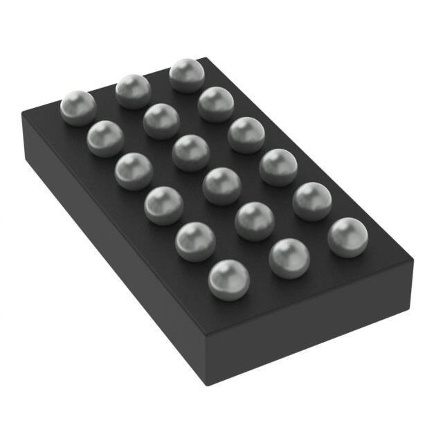
Available in a WLCSP-18(1.35mmX2.55mm)
Package
APPLICATIONS
Tablets
Notebooks
Terminal Displays
All MPS parts are lead-free, halogen-free, and adhere to the RoHS directive. For
MPS green status, please visit the MPS website under Quality Assurance.
“MPS” and “The Future of Analog IC Technology” are registered trademarks of
Monolithic Power Systems, Inc.
Full protection features include recoverable
over-current protection (OCP), over-voltage
protection (OVP), over-temperature protection
(OTP), and short and open protection of any
string on the LED.
The MP3366 is available in a WLCSP18(1.35mmx2.55mm) package.
MP3366 Rev. 1.0
4/11/2016
www.MonolithicPower.com
MPS Proprietary Information. Patent Protected. Unauthorized Photocopy and Duplication Prohibited.
© 2016 MPS. All Rights Reserved.
1
�MP3366 ― STEP-UP, 6-STRING, WHITE LED DRIVER
TYPICAL APPLICATION
L1
D1
VOUT
VIN
C2
C1
GND
R1
COMP
LED4
String 6
String 5
String 3
LED2
LED5
C3
OVP
LED1
LED6
AGND
ISET
R4
String 4
PGND
MP3366
LED3
PWM
String 2
PGND
EN
PWM
LX1
LX2
VIN
VCC
EN
String 1
R2
C4
R3
MP3366 Rev. 1.0
4/11/2016
www.MonolithicPower.com
MPS Proprietary Information. Patent Protected. Unauthorized Photocopy and Duplication Prohibited.
© 2016 MPS. All Rights Reserved.
2
�MP3366 ― STEP-UP, 6-STRING, WHITE LED DRIVER
ORDERING INFORMATION
Part Number*
Package
Top Marking
MP3366GC
WLCSP-18
(1.35mmx2.55mm)
See Below
* For Tape & Reel, add suffix –Z (e.g. MP3366GC–Z)
TOP MARKING
AMZ: Product code of MP3366GC
Y: Year code
WW: Week code
LLL: Lot number
PACKAGE REFERENCE
TOP VIEW
A
EN
AGND
PWM
B
VCC
VIN
LED6
C
COMP
ISET
LED5
D
OVP
LED2
LED4
E
LX1
PGND
LED3
F
LX2
PGND
LED1
1
2
3
WLCSP-18
(1.35mmx2.55mm)
MP3366 Rev. 1.0
4/11/2016
www.MonolithicPower.com
MPS Proprietary Information. Patent Protected. Unauthorized Photocopy and Duplication Prohibited.
© 2016 MPS. All Rights Reserved.
3
�MP3366 ― STEP-UP, 6-STRING, WHITE LED DRIVER
ABSOLUTE MAXIMUM RATINGS(1)
Thermal Resistance
VPWM, VEN, VIN .............................. -0.3V to +30V
VCC ............................................ -0.3V to +6.5V
VLX, VLED1 to VLED6 ........................... -1V to +50V
All other pins .................................. -0.3V to +6V
Junction temperature ............................... 150°C
Lead temperature .................................... 260°C
(2)
Continuous power dissipation (TA = 25°C)
WLCSP-18(1.35mmx2.55mm) ...................1.7W
WLCSP-18(1.35mmx2.55mm)..70…1…..°C/W
Recommended Operating Conditions
(3)
Supply voltage (VIN) ........................... 3V to 25V
Operating junction temp. .......... -40°C to +125°C
MP3366 Rev. 1.0
4/11/2016
(4)
θJA
θJC
NOTES:
1) Exceeding these ratings may damage the device.
2) The maximum allowable power dissipation is a function of the
maximum junction temperature TJ (MAX), the junction-toambient thermal resistance θJA, and the ambient temperature
TA. The maximum allowable continuous power dissipation at
any ambient temperature is calculated by PD (MAX) = (TJ
(MAX)-TA)/θJA. Exceeding the maximum allowable power
dissipation produces an excessive die temperature, causing
the regulator to go into thermal shutdown. Internal thermal
shutdown circuitry protects the device from permanent
damage.
3) The device is not guaranteed to function outside of its
operating conditions.
4) Measured on JESD51-7, 4-layer PCB.
www.MonolithicPower.com
MPS Proprietary Information. Patent Protected. Unauthorized Photocopy and Duplication Prohibited.
© 2016 MPS. All Rights Reserved.
4
�MP3366 ― STEP-UP, 6-STRING, WHITE LED DRIVER
ELECTRICAL CHARACTERISTICS
VIN = 3.7V, VEN = VIN, TA = 25°C, unless otherwise noted.
Parameters
Symbol
Condition
Operating input voltage
VIN
Supply current (quiescent)
IQ
No load
Supply current (shutdown)
IST
VEN = 0V
LDO output voltage
VCC
VCC UVLO threshold
VIN_UVLO
Min
3
6V < VIN < 25V,
0 < IVCC < 10mA
Rising edge
Units
25
V
mA
1
μA
4.5
5
5.5
V
2.42
2.57
2.72
V
80
EN on threshold
VEN_ON
VEN rising
EN off threshold
VEN_OFF
VEN falling
Step-Up Converter
SW on resistance
RDS_ON
IDS = 20mA
SW leakage current
ISW_LK
VSW = 45V
Switching frequency
FSW
Maximum duty cycle
DMAX
ISW_LIMIT
COMP transconductance
Max
1.6
VCC UVLO hysteresis
SW current limit
Typ
GCOMP
mV
1.5
V
0.18
0.8
V
0.3
Ω
1
μA
600
90
93
kHz
96
%
Duty = 90%
2.5
A
∆ICOMP = ±10μA
100
μA/V
Current Dimming
PWM input low threshold
VPWM_LO
VPWM falling
PWM input high threshold
PWM dimming output
frequency
PWM dimming input transfer
point
PWM dimming transfer point
hysteresis
VPWM_HI
VPWM rising
PWM leakage current
IPWM_LK
FPWMO
0.4
1.5
V
23.5k
VPWM = 5V
V
29.5k
Hz
25
%
0.2
%
10
VPWM = 0V
15
μA
1
μA
20.6
mA
1.5
%
45
mA
LED Current Regulation
LEDX average current
ILED
(5)
Current matching
Maximum LED current per
string
ISET regulation voltage
ILEDmax
LEDX regulation voltage
VLEDX
MP3366 Rev. 1.0
4/11/2016
RISET = 62kΩ
19.4
20
ILED = 20mA
ILED = 20mA
1.205
1.235
1.265
V
400
500
600
mV
www.MonolithicPower.com
MPS Proprietary Information. Patent Protected. Unauthorized Photocopy and Duplication Prohibited.
© 2016 MPS. All Rights Reserved.
5
�MP3366 ― STEP-UP, 6-STRING, WHITE LED DRIVER
ELECTRICAL CHARACTERISTICS (continued)
VIN = 3.7V, VEN = VIN, TA = 25°C, unless otherwise noted.
Parameters
Symbol
Condition
Min
Typ
Max
Units
Protection
Over-voltage protection
threshold
OVP UVLO threshold
VOVP_OV
Rising edge
1.13
1.2
1.29
V
VOVP_UV
Step-up converter fails
40
75
105
mV
LEDX over-voltage threshold
VLEDX_OV
VIN > 5.5V
5
5.5
6
V
LEDX UVLO threshold
VLEDX_UV
160
265
360
mV
Thermal shutdown threshold
TST
150
°C
20
°C
Thermal shutdown hysteresis
LEDX over-voltage fault timer
FS = 600kHz
2.4
3.2
4
ms
NOTE:
5) Matching is defined as the difference of the maximum to minimum current divided by 2 times average current.
MP3366 Rev. 1.0
4/11/2016
www.MonolithicPower.com
MPS Proprietary Information. Patent Protected. Unauthorized Photocopy and Duplication Prohibited.
© 2016 MPS. All Rights Reserved.
6
�MP3366 ― STEP-UP, 6-STRING, WHITE LED DRIVER
TYPICAL PERFORMANCE CHARACTERISTICS
VIN = 7V, VEN = 5V, 8 LEDs in series, 6 strings, 20mA/string, TA = 25°C, unless otherwise noted.
MP3366 Rev. 1.0
4/11/2016
www.MonolithicPower.com
MPS Proprietary Information. Patent Protected. Unauthorized Photocopy and Duplication Prohibited.
© 2016 MPS. All Rights Reserved.
7
�MP3366 ― STEP-UP, 6-STRING, WHITE LED DRIVER
TYPICAL PERFORMANCE CHARACTERISTICS (continued)
VIN = 7V, VEN = 5V, 8 LEDs in series, 6 strings, 20mA/string, TA = 25°C, unless otherwise noted.
MP3366 Rev. 1.0
4/11/2016
www.MonolithicPower.com
MPS Proprietary Information. Patent Protected. Unauthorized Photocopy and Duplication Prohibited.
© 2016 MPS. All Rights Reserved.
8
�MP3366 ― STEP-UP, 6-STRING, WHITE LED DRIVER
PIN FUNCTIONS
Package
Pin #
Name
Description
A1
A2
EN
AGND
Enable control input. EN is weakly pulled low internally.
Analog ground.
A3
PWM
B1
VCC
B2
VIN
B3
LED6
C1
COMP
C2
ISET
C3
LED5
D1
OVP
D2
LED2
D3
LED4
E1, F1
LX1/2
E2, F2
PGND
E3
LED3
F3
LED1
MP3366 Rev. 1.0
4/11/2016
PWM signal input. Apply a PWM signal on PWM for brightness control. It is recommended
to use the dimming signal with 100Hz to 20kHz. PWM is weakly pulled low internally.
Internal 5V linear regulator output. VCC provides a power supply for the internal MOSFET
switch gate driver and the internal control circuitry. Bypass VCC to GND with a ceramic
capacitor. If VIN is less than 5.5V, tie VIN and VCC together.
Power supply input. VIN supplies power to the IC. Drive VIN with a 3V-to-25V power
source. VIN must be bypassed locally.
LED string 6 current input. LED6 is the open-drain output of an internal dimming control
switch. Connect the LED string 6 cathode to LED6.
Step-up converter compensation. COMP is used to compensate for the regulation control
loop. Connect a capacitor or a series RC network from COMP to GND.
LED current setting. Tie a current setting resistor from ISET to ground to program the
current in each LED string.
LED string 5 current input. LED5 is the open-drain output of an internal dimming control
switch. Connect the LED string 5 cathode to LED5.
Over-voltage protection input. Connect a resistor divider from the output to OVP to
program the OVP threshold.
LED string 2 current input. LED2 is the open-drain output of an internal dimming control
switch. Connect the LED string 2 cathode to LED2.
LED string 4 current input. LED4 is the open-drain output of an internal dimming control
switch. Connect the LED string 4 cathode to LED4.
Step-up converter power switch output. LX1/2 is the drain of the internal MOSFET switch.
Connect the power inductor and output rectifier to LX1. LX1 and LX2 should be shorted
externally.
Step-up converter power ground.
LED string 3 current input. LED3 is the open-drain output of an internal dimming control
switch. Connect the LED string 3 cathode to LED3.
LED string 1 current input. LED1 is the open-drain output of an internal dimming control
switch. Connect the LED string 1 cathode to LED1.
www.MonolithicPower.com
MPS Proprietary Information. Patent Protected. Unauthorized Photocopy and Duplication Prohibited.
© 2016 MPS. All Rights Reserved.
9
�MP3366 ― STEP-UP, 6-STRING, WHITE LED DRIVER
BLOCK DIAGRAM
VIN
L
LED+
D
COUT
CIN
PGND
VIN
VCC
LX
Regulator
Control
Logic
AGND
EN
BG&Logic
Oscillator
OVP
5.5V
1.2V
LED Short
Protection
600mV
COMP
EA
Max Feedback
Min
Control
LED1
1.235V
ISET
LED2
LED3
Current Control
PWM
Digital Control
LED4
LED5
LED6
Figure 1: Functional Block Diagram
MP3366 Rev. 1.0
4/11/2016
www.MonolithicPower.com
MPS Proprietary Information. Patent Protected. Unauthorized Photocopy and Duplication Prohibited.
© 2016 MPS. All Rights Reserved.
10
�MP3366 ― STEP-UP, 6-STRING, WHITE LED DRIVER
OPERATION
The MP3366 employs a peak current as its
PWM mode architecture and has 6-channel
current sources to regulate the array of 6-string,
white LEDs.
Internal 5V Regulator
The MP3366 has an internal linear regulator
(VCC). When VIN is greater than 5.5V, this
regulator offers a 5V power supply for the
internal MOSFET switch-gate driver and the
internal control circuitry. The VCC voltage drops
to 0V when the chip shuts down. When VIN is
smaller than 5.5V, tie VCC and VIN together.
The MP3366 uses under-voltage lockout
(UVLO) and disables the chip until VCC
exceeds the UVLO threshold. The UVLO
hysteresis is approximately 80mV.
System Start-Up
When enabled, the MP3366 checks the
topology connection first. The chip monitors the
over-voltage protection (OVP) pin to determine
if the Schottky diode is connected or if the boost
output is shorted to GND. An OVP voltage less
than 75mV will fail to switch. The MP3366 also
checks for other safety limits, including UVLO
and over-temperature protection (OTP). If
detections of all protections pass, then the chip
begins boosting the step-up converter with an
internal soft start.
The enable signal should occur after the
establishment of the input voltage and PWM
dimming signal during the start-up sequence to
prevent a large inrush current.
Step-Up Converter
The converter operating frequency is fixed at
600kHz. At the beginning of each switching
cycle, the internal clock turns on the internal
MOSFET. In normal operation, the minimum
turn-on time is 100ns. A stabilizing ramp added
to the output of the current sense amplifier
prevents subharmonic oscillations for duty
cycles greater than 50%. The error amplifier
and ramp voltages are fed into the PWM
comparator. When the compared voltage
reaches the output voltage of the error amplifier
(VCOMP), the internal MOSFET turns off.
MP3366 Rev. 1.0
4/11/2016
The output voltage of the internal error amplifier
is an amplified signal of the difference between
the reference voltage and the feedback voltage.
The converter automatically chooses the lowest
active LEDX voltage to provide a high enough
bus voltage to power all of the LED arrays.
If the feedback voltage drops below the
reference, the output of the error amplifier
increases. More current flows through the
MOSFET, increasing the power delivered to the
output. This forms a closed loop that regulates
the output voltage.
Under light-load operations, especially in the
case of VOUT ≈ VIN, the converter runs in pulseskip mode, where the MOSFET turns on for a
minimum on time of approximately 100ns
before the converter discharges the power to
the output for the remaining period. The
external MOSFET remains off until the output
voltage needs to be boosted again.
Dimming Control
The MP3366 works in combined analog and
PWM dimming mode with 25% as its transfer
point. A PWM signal is applied to the PWM pin.
When the duty cycle of the PWM dimming
signal is greater than or equal to 25%, the IC
dims the LED current with analog mode, and
the LED current amplitude equals ISET*DDIM,
where ISET is the LED current set by a resistor
connected to ISET, and DDIM is the duty cycle of
the PWM dimming signal. Analog dimming
helps reduce LED power loss and prevents
audible noise.
When the duty cycle of the PWM dimming
signal is less than 25%, the IC dims the LED
current in PWM mode. The LED current
amplitude is fixed to 25%*ISET, while the LED
dimming duty is four times DDIM to make the
actual average LED current equal to ISET*DDIM.
The actual LED current dimming frequency is
transferred to the range of 23.5kHz~29.5kHz
from 100Hz~20kHz of the input PWM dimming
signal frequency. This way, the MP3366
improves the low LED current dimming ratio
and prevents audible noise.
www.MonolithicPower.com
MPS Proprietary Information. Patent Protected. Unauthorized Photocopy and Duplication Prohibited.
© 2016 MPS. All Rights Reserved.
11
�MP3366 ― STEP-UP, 6-STRING, WHITE LED DRIVER
Output Over-Voltage Protection (OVP) and
Short Protection
In some unexpected cases, to prevent the IC
from continuously charging the output voltage,
the MP3366 uses an over-voltage protection
(OVP) function to protect the components from
being damaged by the output voltage. If the
OVP high protection threshold point (1.2V) is
reached, the chip stops switching and the
output voltage drops. The switching resumes if
the OVP point drops below the recovery
threshold.
The MP3366 can also achieve an output short
to GND or diode open protection by detecting
the OVP voltage. The IC works in normal
switching operation only when the OVP voltage
is higher than 75mV.
Open-String Protection
Open-string protection is achieved by detecting
both the OVP pin and the LED (1 to 6) pins. If
one or more strings (but not all strings) are
open, the respective LEDX pins are pulled to
ground and the IC continues charging the
output voltage until OVP reaches the 1.2V
protection threshold. The chip stops switching
and marks off the open strings that have an
LEDX pin voltage lower than 265mV. Once
marked, the remaining LED strings force the
output voltage back into its correct regulation.
The string with the largest voltage drop
determines the output regulation. The markedoff strings can also resume normal operation
after they are connected back to the system.
Short-String Protection
The MP3366 monitors the LEDX voltage to
determine if a short string occurs. If one or
more strings are short, the respective LEDX
pins are pulled up to the boost output and
tolerate high voltage stress. If the LEDX voltage
is higher than 5.5V, the short-string condition is
detected on the respective string. When the
short-string fault (LEDX over-voltage fault)
continues for more than 3.2ms, the
corresponding string current regulator is
disabled and disconnects from the output
voltage loop regulation. The LED string
resumes normal current regulation when the
short condition is removed.
Thermal Shutdown
To prevent the IC from operating at exceedingly
high temperatures, thermal shutdown is
implemented by detecting the silicon die
temperature. When the die temperature
exceeds the upper threshold (TST), the IC shuts
down and resumes normal operation when the
die temperature drops below its lower threshold.
Typically, the hysteresis value is 20°C.
If all six strings are open (LED bar is open), the
IC continues charging the output voltage until
the OVP voltage reaches the 1.2V threshold,
and the LED current regulator is marked off.
The IC resumes normal current regulation until
VIN or EN is reset.
MP3366 Rev. 1.0
4/11/2016
www.MonolithicPower.com
MPS Proprietary Information. Patent Protected. Unauthorized Photocopy and Duplication Prohibited.
© 2016 MPS. All Rights Reserved.
12
�MP3366 ― STEP-UP, 6-STRING, WHITE LED DRIVER
APPLICATION INFORMATION
Setting the LED Current
The current of each string is identical and set
through the current setting resistor on ISET,
which can be determined with Equation (1):
1.24(V)
(1)
ISET 1000
RSET (k)
When RSET = 62kΩ, set the LED current to 20mA.
ISET cannot be open.
Selecting the Input Capacitor
The input capacitor reduces the surge current
drawn from the input supply and the switching
noise from the device. The input capacitor
impedance at the switching frequency should be
less than the input source impedance to prevent
the high-frequency switching current from
passing through to the input. Ceramic capacitors
with X5R or X7R dielectrics are recommended
for their low ESR and small temperature
coefficients. For most applications, a 4.7μF
ceramic capacitor is sufficient.
Selecting the Inductor
The MP3366 requires an inductor to supply a
higher output voltage while being driven by the
input voltage. A larger value inductor results in
less ripple current, a lower peak inductor current,
and less stress on the internal N-channel
MOSFET. However, a larger value inductor also
has a larger physical size, higher series
resistance, and lower saturation current.
Choose an inductor that does not saturate under
worst-case load conditions. Select the minimum
inductor value to ensure that the boost converter
works in continuous conduction mode with high
efficiency and good EMI performance.
Calculate the required inductance value using
Equation (2) and Equation (3):
L
η VOUT D (1 D)2
2 fSW ILOAD
D 1
VIN
VOUT
(2)
(3)
Where VIN and VOUT are the input and output
voltages, fSW is the switching frequency, ILOAD is
the LED load current, and η is the efficiency.
MP3366 Rev. 1.0
4/11/2016
With a given inductor value, the inductor DC
current rating is at least 40% higher than the
maximum input peak inductor current for most
applications. The inductor’s DC resistance should
be as small as possible to achieve higher
efficiency.
Selecting the Output Capacitor
The output capacitor keeps the output voltage
ripple small and ensures feedback loop stability.
The output capacitor impedance must be low at
the switching frequency. Ceramic capacitors with
X7R dielectrics are recommended for their low
ESR characteristics. For most applications, a
2.2μF ceramic capacitor is sufficient.
Setting the Over-Voltage Protection (OVP)
The open string protection is achieved through
the detection of the voltage on OVP. In some
unexpected cases, the part continues boosting
the output voltage higher and higher. If the output
voltage reaches the programmed OVP threshold,
the protection is triggered.
To ensure that the chip functions properly, select
the resistor values for the OVP resistor divider to
provide an appropriate set voltage. The
recommended OVP point is about 1.1 to 1.2
times higher than the output voltage for normal
operation. The OVP voltage can be calculated
with Equation (4):
VOVP 1.2(V) (1
RHIGH
)
RLOW
(4)
PCB Layout Guidelines
Efficient PBC layout is critical for stable
operation. Proper layout of the high frequency
switching path can prevent noise and
electromagnetic interference. For best results,
follow the guidelines below.
1. Keep the loop of LX to PGND (U1), output
diode (D1), and output capacitor as short as
possible, since the loop is flowing with high
frequency pulse current.
2. In order to reduce the noise affection, it is
recommend
to
separate
the
power
ground(PGND) and analog ground(AGND),
then connect PGND and AGND together.
www.MonolithicPower.com
MPS Proprietary Information. Patent Protected. Unauthorized Photocopy and Duplication Prohibited.
© 2016 MPS. All Rights Reserved.
13
�MP3366 ― STEP-UP, 6-STRING, WHITE LED DRIVER
PRELIMINARY SPECIFICATIONS SUBJECT TO CHANGE
TYPICAL APPLICATION CIRCUITS
Figure 2: VIN > 5.5V, 6-String, 20mA/String Application
Figure 3: VIN < 5.5V, 6-String, 20mA/String Application
NOTE: Tie VIN and VCC together. Some components are reasonably adjustable based on real cases.
MP3366 Rev. 1.0
4/11/2016
www.MonolithicPower.com
MPS Proprietary Information. Patent Protected. Unauthorized Photocopy and Duplication Prohibited.
© 2016 MPS. All Rights Reserved.
14
�MP3366 ― STEP-UP, 6-STRING, WHITE LED DRIVER
PRELIMINARY SPECIFICATIONS SUBJECT TO CHANGE
PACKAGE INFORMATION
WLCSP-18(1.35mmx2.55mm)
PIN 1 ID
PIN 1 ID
MARKING
PIN 1 ID
INDEX AREA
BOTTOM VIEW
TOP VIEW
SIDE VIEW
NOTE:
1) ALL DIMENSIONS ARE IN MILLIMETERS.
2) BALL COPLANARITY SHALL BE 0.05
MILLIMETER MAX.
3) JEDEC REFERENCE IS MO-211.
4) DRAWING IS NOT TO SCALE.
RECOMMENDED LAND PATTERN
NOTICE: The information in this document is subject to change without notice. Please contact MPS for current specifications.
Users should warrant and guarantee that third party Intellectual Property rights are not infringed upon when integrating MPS
products into any application. MPS will not assume any legal responsibility for any said applications.
MP3366 Rev. 1.0
4/11/2016
www.MonolithicPower.com
MPS Proprietary Information. Patent Protected. Unauthorized Photocopy and Duplication Prohibited.
© 2016 MPS. All Rights Reserved.
15
�


 工商网监
湘ICP备2023018690号
工商网监
湘ICP备2023018690号
