MP6523
Triple Half-Bridge Motor Driver
with Serial Input Control
DESCRIPTION
FEATURES
The MP6523 is a triple, half-bridge, DMOS,
output driver with integrated power MOSFETs
that can drive up to three different loads.
Up to 0.9A Output Current
RDS(ON) (HS + LS) Typically 1.1Ω at 25°C,
Maximum 2Ω at 150°C
Very Low Quiescent Current IVS < 6μA in
Standby Mode Versus Total Temperature
Range
Outputs Short-Circuit Protection
Over-Temperature Protection and PreWarning
Under-Voltage Protection (UVP)
Serial Data Interface
Various Diagnostic Functions: Shorted
Output, Open-Load, Over-Temperature, and
Under-Voltage
Fault Output Flag
Daisy Chaining Possible
Serial Interface Clock Frequency up to
3MHz, 3.3V and 5V Compatible
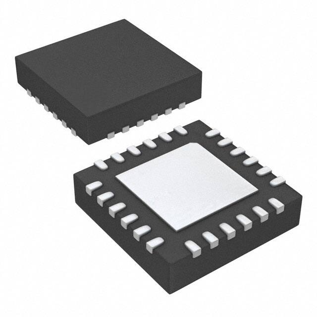
Available in a QFN-24 (4mmx4mm)
Package
The three half-bridges can be controlled
separately from a standard serial data interface
and has various diagnostic functions. The
MP6523 has very low quiescent current in
standby mode, making it suitable for a wide
range of applications.
Full protection features include short-circuit
protection (SCP), under-voltage protection
(UVP), and thermal shutdown.
The MP6523 requires a minimal number of
readily available, standard, external components
and is available in a QFN-24 (4mmx4mm)
package.
APPLICATIONS
Drives Various Loads in Automotive and
Industrial Applications
DC Motors
All MPS parts are lead-free, halogen-free, and adhere to the RoHS directive. For
MPS green status, please visit the MPS website under Quality Assurance. “MPS”
and “The Future of Analog IC Technology” are registered trademarks of Monolithic
Power Systems, Inc.
TYPICAL APPLICATION
VS
DI
MCU
OUT1
CLK
DO
EN
FAULT
Vbatt
VS
CS
M
MP6523
OUT2
M
VCC 5V
OUT3
VCC
AGND
MP6523 Rev. 1.1
7/28/2020
PGND
www.MonolithicPower.com
MPS Proprietary Information. Patent Protected. Unauthorized Photocopy and Duplication Prohibited.
© 2020 MPS. All Rights Reserved.
1
�MP6523 – TRIPLE HALF-BRIDGE MOTOR DRIVER WITH SERIAL INPUT CONTROL
ORDERING INFORMATION
Part Number*
Package
Top Marking
MP6523GR
QFN-24 (4mmx4mm)
See Below
*For Tape & Reel, add suffix –Z (e.g. MP6523GR–Z)
TOP MARKING
MPS: MPS prefix
Y: Year code
WW: Week code
MP6523: Product code of MP6523GR
LLLLLL: Lot number
PACKAGE REFERENCE
TOP VIEW
QFN-24 (4mmx4mm)
MP6523 Rev. 1.1
7/28/2020
www.MonolithicPower.com
MPS Proprietary Information. Patent Protected. Unauthorized Photocopy and Duplication Prohibited.
© 2020 MPS. All Rights Reserved.
2
�MP6523 – TRIPLE HALF-BRIDGE MOTOR DRIVER WITH SERIAL INPUT CONTROL
PIN FUNCTIONS
Pin #
Name
1
2, 3, 4, 5
OUT2
VS
Description
Half-bridge output 2.
Power supply.
6, 11, 23
7, 9, 10, 21, 22, 24
8
NC
PGND
OUT1
12
EN
13
14
DO
VCC
15
FAULT
16
17
AGND
CS
No connection.
Power ground.
Half-bridge output 1.
Enable. Drive EN low for standby mode. Drive EN high for normal
operation.
Serial data output.
Logic supply voltage.
Fault output. A low output at FAULT indicates that the IC has detected an
over-temperature or over-current condition. This output is open-drain.
Analog ground.
Chip select input.
18
19
20
CLK
DI
OUT3
Serial clock input.
Serial data input.
Half-bridge output 3.
ABSOLUTE MAXIMUM RATINGS (1)
Thermal Resistance (4)
Supply voltage (VVS) ....................................40V
VOUTx ...................................... -0.3 to VVS + 0.3V
Logic supply voltage (VVCC) ......... -0.3V to +6.5V
Logic input voltage ............... -0.3 to VVCC + 0.3V
Logic output voltage............. -0.3 to VVCC + 0.3V
Voltage at all other pins .............. -0.3V to +6.5V
Continuous power dissipation (TA = +25°C) (2)
QFN-24 (4mmx4mm) ....................................3W
Junction temperature ............................... 150°C
Lead temperature .................................... 260°C
Storage temperature .................. -60°C to 150°C
QFN-24 (4mmx4mm) ............ 42 ........ 9 .... °C/W
Recommended Operating Conditions (3)
θJA
θJC
NOTES:
1) Exceeding these ratings may damage the device.
2) The maximum allowable power dissipation is a function of the
maximum junction temperature TJ (MAX), the junction-toambient thermal resistance θJA, and the ambient temperature
TA. The maximum allowable continuous power dissipation at
any ambient temperature is calculated by PD (MAX) = (TJ
(MAX)-TA)/θJA. Exceeding the maximum allowable power
dissipation produces an excessive die temperature, causing
the regulator to go into thermal shutdown. Internal thermal
shutdown circuitry protects the device from permanent
damage.
3) The device is not guaranteed to function outside of its operating
conditions.
4) Measured on JESD51-7, 4-layer PCB.
Supply voltage (VVS) .......................... 7V to 28V
Logic supply voltage (VVCC) ........ 3.15V to 5.25V
Operating junction temp. (TJ) ... -40°C to +150°C
MP6523 Rev. 1.1
7/28/2020
www.MonolithicPower.com
MPS Proprietary Information. Patent Protected. Unauthorized Photocopy and Duplication Prohibited.
© 2020 MPS. All Rights Reserved.
3
�MP6523 – TRIPLE HALF-BRIDGE MOTOR DRIVER WITH SERIAL INPUT CONTROL
ELECTRICAL CHARACTERISTICS
7V < VVS < 28V, VVCC = 5V, TA = -40°C to +125°C, unless otherwise noted.
Parameters
Symbol
Operating supply current (VS)
IVS
Condition
Min
VVS < 28V normal operation,
all output stages off
VVS < 28V normal operation,
all output low stages on, no load
VVS < 28V normal operation,
all output high stages on, no load
4.75V < VVCC < 5.25V, normal
operation
VVS = 28V, VVCC = 0V or VVCC =
5V, EN = low, or VVCC = 5V, bit
SE = low, output pins to VS and
GND
Typ
Max
Units
2.2
6
2.65
6
2.7
6
65
90
μA
1.5
6
μA
23
35
μA
3
mA
mA
Operating supply current (VCC)
IVCC
Quiescent current (VS)
IVS
Quiescent current (VCC)
IVCC
4.75V < VVCC < 5.25V, EN or bit
SE = low
Discharge current (VS)
IVS
VVS = 40V, EN = low
Internal oscillator frequency
fOSC
85
120
166
kHz
Power-on reset threshold
VVCC
2.3
2.6
3.0
V
30
100
190
μs
6.5
V
Power-on reset delay
After switching on VVCC
Under-voltage lockout threshold
rising
Under-voltage lockout threshold
hysteresis
Under-voltage lockout delay time
Output Specification
5.5
0.6
7
HS + LS switch-on resistance
RDS(ON)
Inductive shutdown energy (6)
Over-current limit
IOCP
Over-current shutdown delay time
Open-load detection current
Output switch-on/-off delay
OUTx rising time
OUTx falling time
Dead time
MP6523 Rev. 1.1
7/28/2020
TJ = -40°C to +125°C
TJ = +150°C (6)
Bit14 (SCT) = low, VVS = 13V
Bit14 (SCT) = high, VVS = 13V
Bit13 (OLD) = low, output off
VVS = 13V, RLOAD = 50Ω
VVS = 13V, 10% to 90% VOUT,
RLOAD = 50Ω
VVS = 13V, 10% to 90% VOUT,
RLOAD = 50Ω
VVS = 13V, RLOAD = 50Ω
V
14
23
ms
1.1
1.7
2
15
1.8
0.3
Ω
Ω
mJ
A
1
0.1
1.3
0.21
0.28
1.4
0.53
1.9
0.72
2.4
60
mA
μs
2
20
50
μs
2
20
45
μs
2
www.MonolithicPower.com
MPS Proprietary Information. Patent Protected. Unauthorized Photocopy and Duplication Prohibited.
© 2020 MPS. All Rights Reserved.
ms
μs
4
�MP6523 – TRIPLE HALF-BRIDGE MOTOR DRIVER WITH SERIAL INPUT CONTROL
ELECTRICAL CHARACTERISTICS (continued)
7V < VVS < 28V, VVCC = 5V, TA = -40°C to +125°C, unless otherwise noted.
Parameters
Symbol
Condition
Min
Typ
Max
Units
0.8
80
V
V
μA
170
°C
200
°C
°C
°C
EN Input
EN low-level threshold
EN high-level threshold
Pull-down current of EN input
Thermal Shutdown and Pre-Warning (6)
Thermal pre-warning threshold
Thermal pre-warning hysteresis
Thermal shutdown threshold
Thermal shutdown hysteresis
Ratio thermal shutdown/thermal
pre-warning
MP6523 Rev. 1.1
7/28/2020
VEN = VVCC
3
10
1.7
120
145
150
15
175
15
1.05
1.2
www.MonolithicPower.com
MPS Proprietary Information. Patent Protected. Unauthorized Photocopy and Duplication Prohibited.
© 2020 MPS. All Rights Reserved.
5
�MP6523 – TRIPLE HALF-BRIDGE MOTOR DRIVER WITH SERIAL INPUT CONTROL
SERIAL INTERFACE TIMING ELECTRICAL CHARACTERISTICS (6)
7V < VVS < 28V, VVCC = 5V, TA = -40°C to +125°C, unless otherwise noted.
Parameters
Symbol Condition
Min
Typ
Max
Units
0.3 x
VVCC
V
Logic Inputs (DI, CLK, CS)
Input low-level threshold
VDI, VCLK = VVCC
VCS = 0V
0.7 x
VVCC
2
2
0V < VDO < VVCC, VCS = VVCC
VVCC 0.7V
-10
Input high-level threshold
Pull-down current of DI, CLK
Pull-up current of CS
Logic Output (DO)
Output low level
Output high level
Leakage current (tri-state)
Timing Characteristics
T1
T2
50
50
μA
μA
0.5
V
V
10
μA
200
200
100
200
150
150
ns
ns
ns
ns
ns
ns
ms
ms
ns
ns
ns
ns
ns
ns
ns
DO enable after CS falling edge
DO disable after CS rising edge
DO falling/rising time
DO valid time
CS set-up time (high to low)
CS set-up time (low to high)
CDO = 100pF
CDO = 100pF
CDO = 100pF
CDO = 100pF
T10
T4
T8
CS high time
T9
CLK high time
CLK low time
CLK period time
CLK set-up time (high to low)
T5
T6
T7
0.75
0.3
150
150
333
150
CLK set-up time (low to high)
DI set-up time
DI hold time
T3
T11
T12
150
26
26
Bit14 (SCT) = high
Bit14 (SCT) = low
V
NOTES:
5) Guaranteed by characterization, not tested in production.
6) Not subject to production test, specified by design.
MP6523 Rev. 1.1
7/28/2020
www.MonolithicPower.com
MPS Proprietary Information. Patent Protected. Unauthorized Photocopy and Duplication Prohibited.
© 2020 MPS. All Rights Reserved.
6
�MP6523 – TRIPLE HALF-BRIDGE MOTOR DRIVER WITH SERIAL INPUT CONTROL
SERIAL INTERFACE TIMING DIAGRAMS
1
2
CS
DO
9
CS
4
7
CLK
5
3
8
6
DI
11
CLK
10
12
DO
Inputs DI, CLK, CS: High Level = 0.7 x Vcc, Low Level = 0.3 x Vcc
Output DO: High Level = 0.8 x Vcc, Low Level = 0.2 x Vcc
MP6523 Rev. 1.1
7/28/2020
www.MonolithicPower.com
MPS Proprietary Information. Patent Protected. Unauthorized Photocopy and Duplication Prohibited.
© 2020 MPS. All Rights Reserved.
7
�MP6523 – TRIPLE HALF-BRIDGE MOTOR DRIVER WITH SERIAL INPUT CONTROL
TYPICAL PERFORMANCE CHARACTERISTICS
VVS = 13V, VVCC = 5V, TA = 25°C, unless otherwise noted.
MP6523 Rev. 1.1
7/28/2020
www.MonolithicPower.com
MPS Proprietary Information. Patent Protected. Unauthorized Photocopy and Duplication Prohibited.
© 2020 MPS. All Rights Reserved.
8
�MP6523 – TRIPLE HALF-BRIDGE MOTOR DRIVER WITH SERIAL INPUT CONTROL
TYPICAL PERFORMANCE CHARACTERISTICS (continued)
VVS = 13V, VVCC = 5V, TA = 25°C, unless otherwise noted.
MP6523 Rev. 1.1
7/28/2020
www.MonolithicPower.com
MPS Proprietary Information. Patent Protected. Unauthorized Photocopy and Duplication Prohibited.
© 2020 MPS. All Rights Reserved.
9
�MP6523 – TRIPLE HALF-BRIDGE MOTOR DRIVER WITH SERIAL INPUT CONTROL
BLOCK DIAGRAM
Serial interface
Input register Output register
CS
DI
CLK
SRR
TP
n. u.
n. u.
n. u.
n. u.
LS1
SLS1
HS1
SHS1
n. u.
n. u.
n. u.
n. u.
LS2
SLS2
HS2
SHS2
n. u.
n. u.
n. u.
n. u.
LS3
SLS3
GH1
HS Gate
Driver
HS3
SHS3
OLD
SCD
SCT
EN
SE
PSF
GH3
Control Logic
DO
EN
GH2
GL1
LS Gate
Driver
GL2
GL3
Charge
Pump
VS
GH1
GH2
GH3
Power on reset
VCC
OUT1
FAULT
OUT2
Fault
Handling
AGND
OUT3
GL1
UVLO
Comparator
UVLO_REF
Over load
and short
circuit
protection
GL2
GL3
TSD
PGND
VS
Figure 1: Functional Block Diagram
MP6523 Rev. 1.1
7/28/2020
www.MonolithicPower.com
MPS Proprietary Information. Patent Protected. Unauthorized Photocopy and Duplication Prohibited.
© 2020 MPS. All Rights Reserved.
10
�MP6523 – TRIPLE HALF-BRIDGE MOTOR DRIVER WITH SERIAL INPUT CONTROL
OPERATION
The MP6523 is a three, half-bridge, motor driver
that can drive up to three different loads with
separate controls for high-side or low-side
MOSFETs from a standard serial data interface.
The output data at DO is enabled on the falling
edge of CS. The output data changes state with
the rising edge of CLK and remains stable until
the next rising edge of CLK appears. When CS
is high, DO is in a tri-state condition. The LSB
(bit0, TP) is transferred first.
Serial Interface
Data transfer starts with the falling edge of the
CS signal (see Figure 2). Execution of new input
data is enabled on the rising edge of the CS
signal. Data must appear at DI synchronized to
CLK and is accepted on the falling edge of the
CLK signal. The LSB (bit0, SRR) must be
transferred first.
CS
DI
SRR
0
n.u.
1
n.u.
2
LS1
HS1
3
4
SLS1
SHS1
n.u.
5
n.u.
6
LS2
HS2
7
8
SLS2
SHS2
n.u.
9
n.u.
10
LS3
11
HS3
12
OLD
13
SCT
14
SE
15
CLK
DO
DO
TP
n.u.
n.u.
n.u.
n.u.
n.u.
n.u.
SLS3
SHS3
SCD
EN
PSF
Figure 2: Data Transfer
Table 1: Input Data Protocol
Bit
Input Register
0
SRR
1
2
3
4
5
6
7
8
9
10
11
12
13
n. u.
n. u.
LS1
HS1
n. u.
n. u.
LS2
HS2
n. u.
n. u.
LS3
HS3
OLD
14
SCT
15
SE
MP6523 Rev. 1.1
7/28/2020
Function
Status register reset (high = reset; the bits PSF, SCD and over-temperature
shutdown in the output data register are set to low).
Not used.
Not used.
Controls output LS1 (high = switch output LS1 on).
Controls output HS1 (high = switch output HS1 on).
Not used.
Not used.
Controls output LS2 (high = switch output LS2 on).
Controls output HS2 (high = switch output HS2 on).
Not used.
Not used.
Controls output LS3 (high = switch output LS3 on).
Controls output HS3 (high = switch output HS3 on).
Open-load detection (low = on).
Programmable time delay for short circuit (shutdown delay high/low =
12ms/1.5ms).
Software enable. Low = standby, high = normal operation (data transfer is not
affected by standby function because the digital part is still powered).
www.MonolithicPower.com
MPS Proprietary Information. Patent Protected. Unauthorized Photocopy and Duplication Prohibited.
© 2020 MPS. All Rights Reserved.
11
�MP6523 – TRIPLE HALF-BRIDGE MOTOR DRIVER WITH SERIAL INPUT CONTROL
Table 2: Output Data Protocol
Bit
Input Register
0
TP
1
2
n. u.
n. u.
3
Status LS1
4
Status HS1
5
6
7
8
9
10
11
12
n. u.
n. u.
Status LS2
Status HS2
n. u.
n. u.
Status LS3
Status HS3
13
SCD
14
EN
15
PSF
Function
Temperature pre-warning: high = warning (over-temperature shutdown see
remark below).
Not used.
Not used.
Normal operation: high = output is on, low = output is off. Open-load detection:
high = open load, low = no open load (correct load condition is detected if the
corresponding output is switched off).
Normal operation: high = output is on, low = output is off. Open-load detection:
high = open load, low = no open load (correct load condition is detected if the
corresponding output is switched off).
Not used.
Not used.
See LS1.
See HS1.
Not used.
Not used.
See LS1.
See HS1.
Short circuit detected. Set SCD high when at least one output is switched off by a
short-circuit condition.
Enable. EN is controlled by software (bit SE in input register) and hardware Enable
(EN). Low = standby, high = normal operation.
Power supply fail. Under-voltage at VS detected.
NOTE: Bit0 to 15 = high: over-temperature shutdown.
Table 3: Status of the Input Register after Power-On Reset
Bit15
(SE)
H
Bit14 Bit13
(SCT) (OLD)
H
MP6523 Rev. 1.1
7/28/2020
H
Bit12
(HS3)
Bit11
(LS3)
Bit10
Bit9
L
L
x
x
Bit8
Bit7
(HS2) (LS2)
L
L
Bit6
Bit5
x
x
Bit4
Bit3
(HS1) (LS1)
L
L
Bit2
Bit1
Bit0
(SRR)
x
x
L
www.MonolithicPower.com
MPS Proprietary Information. Patent Protected. Unauthorized Photocopy and Duplication Prohibited.
© 2020 MPS. All Rights Reserved.
12
�MP6523 – TRIPLE HALF-BRIDGE MOTOR DRIVER WITH SERIAL INPUT CONTROL
Enable Control (EN)
There are two ways to enable or disable the
MP6523:
Controlled by software: set bit SE in the input
register. Low = standby, high = normal
operation.
Hardware enable (EN): low = standby, high =
normal operation.
In both cases, if the device is disabled, then all
output stages are turned off, but the serial
interface remains active. The output stages can
be activated again by setting the bit SE high
(when EN = high) or by switching EN back to
high (when SE = high).
Open-Load Detection
When the open-load detection bit (OLD) is set to
low, open-load detection is enabled. In this mode,
a pull-down current for each low-side switch is
turned on. When an open load has been
detected, the corresponding output bit (LSx or
HSx) in the output data register is set to high.
Once the open-load is removed, the
corresponding DO bit is cleared, indicating the
end of the open-load event.
Testing the open load of an H-bridge
configuration is a two-step process. First, switch
off all high-side (HSx/HSy) and low-side
(LSx/LSy) drivers. The voltage at both clamps in
this condition is pulled down. Next, with both lowside drivers off, switch on one high-side driver
(HSx or HSy). Since the DC motor has a
relatively low internal resistance, the voltage of
the inactive high-side output should be at the
same level as the activated high-side output. In
the case of an open-load, the inactive high-side
output register reports a 0 if the active high-side
output is 1. Conversely, if the load is connected,
the inactive high-side output reports a 1.
Discharge Circuit
Many typical applications use an inverse-polarity
protection diode (see D1 in Figure 3). However,
this method involves a certain danger. During
inhibit mode, the IC consumes only an extremely
low current (IVS), such as 20μA maximum. Any
peaks on the supply voltage charge the blocking
capacitor gradually. D1 prevents the capacitor
from discharging via the power supply. Due to
the extremely small quiescent current,
MP6523 Rev. 1.1
7/28/2020
discharging via the IC can also be neglected.
This means that during long periods in inhibit
mode, the IC's supply voltage could increase
continuously until the maximum supply voltage
limit of 40V is exceeded, damaging the IC. The
device features a discharger circuit that prevents
such unwanted effects. If VS exceeds a
threshold value of approximately 37V, the
blocking capacitor is discharged via an
integrated resistor until VS falls below the
threshold again.
MP6523
D1
C1
Vbatt
Vpk
Figure 3: Functional Principle of the Discharger
Circuit
Over-Current Protection (OCP)
The MP6523 has internal overload and shortcircuit protection. The currents in both the highside and low-side MOSFETs are measured and
if the current exceeds the current limit, an
internal timer is started. When a permanent overcurrent shutdown delay time programmed by the
short-circuit timer bit (SCT) is reached, the shortcircuit detection bit (SCD) is set, and the shorted
output is disabled. By writing a high to the SRR
bit in the input register, the SCD bit is reset, and
the disabled outputs are enabled.
Thermal Shutdown and Pre-Warning
Thermal monitoring is also integrated into the
MP6523. If the junction temperature rises above
the thermal pre-warning threshold, the
temperature pre-warning bit (TP) in the output
register is set. When the temperature falls below
the thermal pre-warning threshold, the bit TP is
reset. The bit TP can be read without transferring
a complete 16-bit data word. When CS = high to
low, the state of TP appears at DO. After the
microcontroller has read this information, CS is
set high and the data transfer is interrupted
without affecting the state of the input and output
registers.
www.MonolithicPower.com
MPS Proprietary Information. Patent Protected. Unauthorized Photocopy and Duplication Prohibited.
© 2020 MPS. All Rights Reserved.
13
�MP6523 – TRIPLE HALF-BRIDGE MOTOR DRIVER WITH SERIAL INPUT CONTROL
If the junction temperature rises above the
thermal shutdown threshold, all switches turn off,
and all bits in the output register are set high.
Operation resumes immediately when the
junction temperature has fallen below the
thermal shutdown threshold and when a high
has been written to the SRR bit in the input
register.
The thermal pre-warning
threshold have hysteresis.
and
shutdown
Note that bit0 to 15 = high indicates an overtemperature shutdown.
Power-Supply Fail
If at any time the voltage on VS falls below the
under-voltage lockout (UVLO) threshold voltage,
an internal timer is started. The power supply fail
MP6523 Rev. 1.1
7/28/2020
bit (PSF) in the output register is set, and all
outputs are disabled when a permanent UVLO
delay time is reached.
Operation resumes immediately when VS rises
above the UVLO threshold. The PSF bit remains
high until it is reset by the SRR bit in the input
register.
Fault Output
The MP6523 includes an open-drain, active-low
fault indicator output (FAULT). A fault is
indicated if the current limit is tripped or thermal
shutdown is tripped. A fault on any channel
causes FAULT to be pulled low. The FAULT
value is maintained until the fault condition is
removed and normal operation resumes. Do not
apply more than 6V to FAULT.
www.MonolithicPower.com
MPS Proprietary Information. Patent Protected. Unauthorized Photocopy and Duplication Prohibited.
© 2020 MPS. All Rights Reserved.
14
�MP6523 – TRIPLE HALF-BRIDGE MOTOR DRIVER WITH SERIAL INPUT CONTROL
PACKAGE INFORMATION
QFN-24 (4mmx4mm)
3.90
4.10
2.50
2.80
19
PIN 1 ID
MARKING
18
3.90
4.10
PIN 1 ID
INDEX AREA
PIN 1 ID
SEE DETAIL A
24
1
0.50
BSC
2.50
2.80
0.18
0.30
6
13
0.35
0.45
TOP VIEW
12
7
BOTTOM VIEW
PIN 1 ID OPTION A
0.30x45º TYP.
PIN 1 ID OPTION B
R0.25 TYP.
0.80
1.00
0.20 REF
0.00
0.05
DETAIL A
SIDE VIEW
3.90
2.70
0.70
0.25
NOTE:
1) ALL DIMENSIONS ARE IN MILLIMETERS.
2) EXPOSED PADDLE SIZE DOES NOT INCLUDE MOLD FLASH.
3) LEAD COPLANARITY SHALL BE 0.10 MILLIMETER MAX.
4) DRAWING CONFIRMS TO JEDEC MO-220, VARIATION VGGD.
5) DRAWING IS NOT TO SCALE.
0.50
RECOMMENDED LAND PATTERN
MP6523 Rev. 1.1
7/28/2020
www.MonolithicPower.com
MPS Proprietary Information. Patent Protected. Unauthorized Photocopy and Duplication Prohibited.
© 2020 MPS. All Rights Reserved.
15
�MP6523 – TRIPLE HALF-BRIDGE MOTOR DRIVER WITH SERIAL INPUT CONTROL
Revision History
Revision #
Revision
Date
Description
Add “3.3V compatible” in Features;
r1.1
7/27/2020
Change recommended operating min. spec of VCC
from 4.75V to 3.15V.
Pages
Updated
1
3
NOTICE: The information in this document is subject to change without notice. Users should warrant and guarantee that third
party Intellectual Property rights are not infringed upon when integrating MPS products into any application. MPS will not assume
any legal responsibility for any said applications.
MP6523 Rev. 1.1
7/28/2020
www.MonolithicPower.com
MPS Proprietary Information. Patent Protected. Unauthorized Photocopy and Duplication Prohibited.
© 2020 MPS. All Rights Reserved.
16
�


 工商网监
湘ICP备2023018690号
工商网监
湘ICP备2023018690号
