MPQ20051
Low Noise, High PSRR, 1A
Linear Regulator
AEC-Q100 Qualified
The Future of Analog IC Technology
DESCRIPTION
FEATURES
The MPQ20051 is a low-dropout linear regulator
that supplies up to 1A current with a 140mV
dropout voltage. The externally-adjustable output
voltage has a range of 0.8V to 5V from an input
voltage of 2.5V to 5.5V.
An internal PMOS pass element allows for a low
130μA ground current, making the MPQ20051
suitable for battery-powered devices. Other
features include low-power shutdown, and shortcircuit and thermal protection.
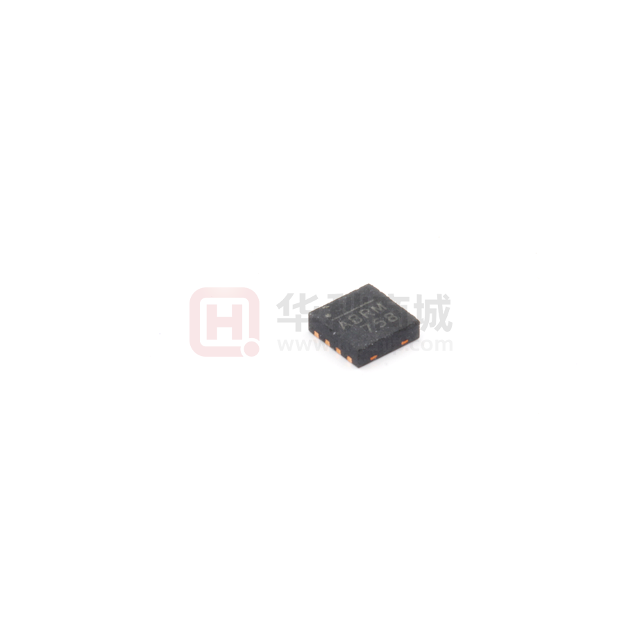
The MPQ20051 is available in 3mm x 3mm 8-pin
QFN package.
Guaranteed Industrial/Automotive Temp
Range Limits
Up to 1A Output Current
Low 140mV Dropout at 1A
Low 130μA Ground Current
Output Voltage Available from 0.8V to 5V
Low Noise: 13μVRMS typical (10Hz to 100kHz)
63dB PSRR @1kHz
Stable with Ceramic Capacitor
Excellent Load/Line Transient Response
Current Limiting and Thermal Protection
Available in 3mm x 3mm 8-pin QFN Package
Available in AEC-Q100 Qualified Grade 1
APPLICATIONS
Automotive/Industrial Power System
Notebook Computers
Cordless Telephones
Cellular Phones
Wireless Communication Equipments
All MPS parts are lead-free and adhere to the RoHS directive. For MPS green
status, please visit MPS website under Quality Assurance. “MPS” and “The
Future of Analog IC Technology” are Registered Trademarks of Monolithic
Power Systems, Inc.
TYPICAL APPLICATION
V IN
VIN
VOUT
R1
MPQ20051
CIN
COUT
FB
2.2 F
4.7 F
R2
V EN
EN
GND
R1
OUT
MPQ20051 Rev. 1.02
www.MonolithicPower.com
10/9/2019
MPS Proprietary Information. Patent Protected. Unauthorized Photocopy and Duplication Prohibited.
© 2019 MPS. All Rights Reserved.
1
�MPQ20051 – LOW NOISE HIGH PSRR 1A LINEAR REGULATOR, AEC-Q100 QUALIFIED
ORDERING INFORMATION
Part Number
MPQ20051DQ-AEC1*
MPQ20051DQ**
Package
QFN-8(3mmx3mm)
QFN-8(3mmx3mm)
Top Marking
MSL Rating
See Below
Level1
* For Tape & Reel, add suffix -Z (e.g. MPQ20051DQ-AEC1-Z)
For RoHS compliant packaging, add suffix –LF (e.g. MPQ20051DQ-AEC1-LF-Z).
** For Tape & Reel, add suffix -Z (e.g. MPQ20051DQ-Z)
For RoHS compliant packaging, add suffix –LF (e.g. MPQ20051DQ-LF-Z).
TOP MARKING
ABR: product code
Y: year code
LLL: lot number
PACKAGE REFERENCE
TOP VIEW
OUT 1
8 IN
OUT 2
7 IN
FB 3
6 NC
GND 4
5 EN
EXPOSED PAD
ON BACKSIDE
CONNECT TO GND
QFN8 (3 x 3mm)
MPQ20051 Rev. 1.02
www.MonolithicPower.com
10/9/2019
MPS Proprietary Information. Patent Protected. Unauthorized Photocopy and Duplication Prohibited.
© 2019 MPS. All Rights Reserved.
2
�MPQ20051 – LOW NOISE HIGH PSRR 1A LINEAR REGULATOR, AEC-Q100 QUALIFIED
ABSOLUTE MAXIMUM RATINGS (1)
Thermal Resistance (5)
VIN, EN, FB to GND ....................... -0.3V to +6V
OUT to GND........................ -0.5V to (VIN + 0.5V)
Continuous Power Dissipation ...... (TA=25°C) (2)
QFN8 (3x3mm) ................................................2.0W
Junction Temperature ............................... 150C
Storage Temperature Range ...... -65°C to 150°C
Lead Temperature (Soldering, 10sec)........... 260°C
QFN-8 (3mmx3mm) ................ 50 ...... 12... °C/W
ESD SUSCEPTIBILITY(3)
HBM (Human Body Mode)........................... 2kV
CDM (Changed Device Mode) .................. 750V
Recommended Operating Conditions (4)
Supply Input Voltage ....................... 2.5V to 5.5V
Enable Input Voltage ......................... 0V to 5.5V
Operating Junction Temp. (TJ). -40°C to +125°C
θJA
θJC
Notes:
1) Exceeding these ratings may damage the device.
2) The maximum allowable power dissipation is a function of the
maximum junction temperature TJ (MAX), the junction-toambient thermal resistance θJA, and the ambient temperature
TA. The maximum allowable continuous power dissipation at
any ambient temperature is calculated by PD (MAX) = (TJ
(MAX)-TA)/θJA. Exceeding the maximum allowable power
dissipation will cause excessive die temperature, and the
regulator will go into thermal shutdown. Internal thermal
shutdown circuitry protects the device from permanent
damage.
3) Devices
are
ESD
sensitive.
Handling
precaution
recommended.
4) The device is not guaranteed to function outside of its
operating conditions.
5) Measured on JESD51-7, 4-layer PCB.
MPQ20051 Rev. 1.02
www.MonolithicPower.com
10/9/2019
MPS Proprietary Information. Patent Protected. Unauthorized Photocopy and Duplication Prohibited.
© 2019 MPS. All Rights Reserved.
3
�MPQ20051 – LOW NOISE HIGH PSRR 1A LINEAR REGULATOR, AEC-Q100 QUALIFIED
ELECTRICAL CHARACTERISTICS
VIN=VOUT+0.5V or VIN=2.5V, EN=VIN, TJ=-40ºC to +125ºC Typical values are at TJ=25°C, unless
otherwise specified
Parameter
Input Voltage
Input Under Voltage Lockout
Hysteresis of UVLO
Condition
FB Voltage
VOUT=0.8V, IOUT=1mA
Min
2.5
1.95
VIN rising
IOUT=1mA, TJ=25°C
IOUT=1mA, -40≤TJ≤125°C
Continuous, VIN≥2.5V, VOUT=2.5V
VOUT=0, VIN≥2.5V
VOUT=2.5V, VOUT within 4% of normal
output voltage VIN=5.5V
IOUT=0.1mA, VOUT=2.5V
IOUT=1A, VOUT=2.5V
IOUT=1A, VOUT=2.5V
IOUT=750mA, VOUT=2.5V
IOUT=500mA, VOUT=2.5V
VOUT=2.5V, VIN from VOUT+0.5V to
5.5V, IOUT=100mA,
IOUT from 100mA to 1A, VOUT=2.5V
VOUT=1.1V
IOUT=100mA, f ranges
VOUT=3.3V
from 10Hz to 100kHz
VOUT=5V
f=100Hz
f=1kHz
VIN = 2.5V, VOUT = 1.1V,
IOUT = 1A
f=10kHz
f=1MHz
TJ=25°C
VIN=+5.5V
-40 ≤TJ
≤125°C
VIN=VEN=+5.5V
VIN=+5.5V, VFB=6V
VOUT(NOM)=2.5V, COUT=4.7μF,
VOUT=10% to 90%VOUT(NOM)
EN Logic High
EN Logic Low
Typical thermal hysteresis =20°C
Output Voltage Accuracy
Maximum Output Current
Short-Circuit Current Limit
In-Regulation Current Limit
Ground Current
Dropout Voltage(6)
Line Regulation(7)
Load Regulation (8)
Output Voltage Noise (9)
PSRR (9)
Shutdown Supply Current
EN Pin Current , Enabled
Feedback Pin Current
Startup Time
EN PIN Threshold
Thermal Shutdown Temperature
TJ=25°C
-40 ≤TJ
≤125°C
(9)
Typ
Max
5.5
2.3
0.784
160
0.8
0.816
0.776
0.8
0.824
2
3
Units
V
V
mV
V
-2
-3
1
1.2
1.6
2.3
A
A
1.4
2.2
3.0
A
130
400
140
105
70
200
700
280
210
140
-0.15
-0.5
13
35
55
65
63
63
33
0.1
%
μA
mV
0.15
%/V
0.5
%
μVRMS
dB
0.3
30
μA
0.1
0.1
0.3
0.3
μA
μA
45
100
μs
1.5
0.4
150
V
°C
Notes:
6) Dropout Voltage is defined as the input to output differential when the output voltage drops 100mV below its nominal value.
VOUT V
7) Line Regulation=
IN(MAX )
VOUT V
IN(MIN)
V
VIN(MIN) VOUT(NOM)
INMAX
8) Load Regulation=
VOUT I
OUT (MAX )
VOUT I
VOUT NOM
OUT (MIN)
(% / V)
(%)
9) Design guarantee, not production test.
MPQ20051 Rev. 1.02
www.MonolithicPower.com
10/9/2019
MPS Proprietary Information. Patent Protected. Unauthorized Photocopy and Duplication Prohibited.
© 2019 MPS. All Rights Reserved.
4
�MPQ20051 – LOW NOISE HIGH PSRR 1A LINEAR REGULATOR, AEC-Q100 QUALIFIED
TYPICAL PERFORMANCE CHARACTERISTICS
VIN = 2.5V, VOUT = 1.1V, CIN=2.2µF, COUT=4.7µF, TA = 25°C, unless otherwise noted.
MPQ20051 Rev. 1.02
www.MonolithicPower.com
10/9/2019
MPS Proprietary Information. Patent Protected. Unauthorized Photocopy and Duplication Prohibited.
© 2019 MPS. All Rights Reserved.
5
�MPQ20051 – LOW NOISE HIGH PSRR 1A LINEAR REGULATOR, AEC-Q100 QUALIFIED
TYPICAL PERFORMANCE CHARACTERISTICS (continued)
VIN = 2.5V, VOUT = 1.1V, CIN=2.2µF, COUT=4.7µF, TA = 25°C, unless otherwise noted.
MPQ20051 Rev. 1.02
www.MonolithicPower.com
10/9/2019
MPS Proprietary Information. Patent Protected. Unauthorized Photocopy and Duplication Prohibited.
© 2019 MPS. All Rights Reserved.
6
�MPQ20051 – LOW NOISE HIGH PSRR 1A LINEAR REGULATOR, AEC-Q100 QUALIFIED
TYPICAL PERFORMANCE CHARACTERISTICS (continued)
VIN = 2.5V, VOUT = 1.1V, CIN=2.2µF, COUT=4.7µF, TA = 25°C, unless otherwise noted.
VOUT
500mV/div.
VOUT
500mV/div.
VOUT
500mV/div.
VIN
1V/div.
VIN
1V/div.
VEN
1V/div.
IOUT
1A/div.
IOUT
1A/div.
IOUT
1A/div.
VOUT
500mV/div.
VOUT
10mV/div.
VOUT
1V/div.
VIN
2V/div.
VEN
1V/div.
IOUT
1A/div.
VIN
2V/div.
VIN
2V/div.
IOUT
1A/div.
VOUT
10mV/div.
IIN
2A/div.
VOUT
500mV/div.
VOUT
1V/div.
IIN
2A/div.
IOUT
500mA/div.
VIN
1V/div.
MPQ20051 Rev. 1.02
www.MonolithicPower.com
10/9/2019
MPS Proprietary Information. Patent Protected. Unauthorized Photocopy and Duplication Prohibited.
© 2019 MPS. All Rights Reserved.
7
�MPQ20051 – LOW NOISE HIGH PSRR 1A LINEAR REGULATOR, AEC-Q100 QUALIFIED
PIN FUNCTIONS
Pin #
Name
Pin Function
1, 2
VOUT
Regulator output. Bypass with a standard 4.7μF ceramic capacitor to GND. Connect all
the pins together externally.
3
FB
Feedback Input. Connect FB to the center point of the external resistor divider. The
feedback threshold voltage is 0.8V.
4
GND
Ground. Connect exposed pad to GND plane for optimal thermal performance.
Exposed pad
5
EN
Regulator Enable Control Input. Drive EN above 1.5V to turn on the MPQ20051. Drive
EN below 0.4V to turn it off. Do not float the EN pin.
6
NC
No Connection. Leave this NC pin open.
7, 8
VIN
Regulator Input. Supply voltage ranges from 2.5V to 5.5V. Bypass with 2.2μF capacitor.
These pins must be externally connected for proper operation even if they are internally
connected.
MPQ20051 Rev. 1.02
www.MonolithicPower.com
10/9/2019
MPS Proprietary Information. Patent Protected. Unauthorized Photocopy and Duplication Prohibited.
© 2019 MPS. All Rights Reserved.
8
�MPQ20051 – LOW NOISE HIGH PSRR 1A LINEAR REGULATOR, AEC-Q100 QUALIFIED
FUNCTIONAL BLOCK DIAGRAM
VIN
UVLO
Vreference
EA
VOUT
EN
GND
FB
Figure 1—Functional Block Diagram
MPQ20051 Rev. 1.02
www.MonolithicPower.com
10/9/2019
MPS Proprietary Information. Patent Protected. Unauthorized Photocopy and Duplication Prohibited.
© 2019 MPS. All Rights Reserved.
9
�MPQ20051 – LOW NOISE HIGH PSRR 1A LINEAR REGULATOR, AEC-Q100 QUALIFIED
OPERATION
The MPQ20051 is a low-dropout linear regulator
that can supply up to 1A current, which makes it
suitable for very low voltage, low quiescent, low
noise, and high PSRR applications such as
wireless LAN transceivers, notebook computers,
smartphones, and other low-power electronics.
The MPQ20051 uses an internal PMOS as the
pass element and includes both thermal
shutdown and an internal current-limiting circuit.
Dropout Voltage
Dropout voltage is the minimum input to output
differential voltage required for the regulator to
maintain an output voltage within 100mV of its
nominal value. Because the PMOS pass element
behaves as a low-value resistor, the dropout
voltage of MPQ20051 is only 140mV.
Shutdown
The MPQ20051 can be switched ON or OFF by a
logic input at the EN pin: Logic high turns the
regulator on and logic low turns it off. Tie the EN
pin to VIN if the application does not require the
shutdown feature. Do not float the EN pin.
Current Limit
The MPQ20051 includes a current limit structure
that monitors and controls the PMOS gate
voltage to limit the guaranteed maximum output
current to 1.6A.
Thermal Protection
Thermal protection turns off the PMOS when the
junction temperature exceeds 150°C, allowing
the IC to cool. When the IC’s junction
temperature drops by 20°C, the PMOS will turn
on again. Thermal protection limits total power
dissipation in the MPQ20051. For reliable
operation, limit the junction temperature to a
maximum of 125°C.
Load-Transient Considerations
The output response of the load-transient
consists of a transient response and DC shift—
the MPQ20051’s excellent load regulation
effectively limits the DC shift. The output voltage
transient depends on the output capacitor’s value
and ESR. Increasing the capacitance and
decreasing the ESR will improve the transient
response.
MPQ20051 Rev. 1.02
www.MonolithicPower.com
10/9/2019
MPS Proprietary Information. Patent Protected. Unauthorized Photocopy and Duplication Prohibited.
© 2019 MPS. All Rights Reserved.
10
�MPQ20051 – LOW NOISE HIGH PSRR 1A LINEAR REGULATOR, AEC-Q100 QUALIFIED
APPLICATION INFORMATION
Setting the Output Voltage
The MPQ20051 has an externally-set output
voltage with a range of 0.8V to 5V given a 2.5V
to 5.5V input. Set the output voltage using a
resistive voltage divider from the output voltage
to the FB pin. The result of the voltage divider at
the FB pin is:
VFB VOUT
R2
R1 R2
Where VFB is the feedback threshold voltage (VFB
= 0.8V), and VOUT is the output voltage. Thus the
output voltage is:
VOUT 0.8
R1 R2
R2
R2 can go as high as 100kΩ, but typical
applications use 10kΩ. After selecting R2, R1 is
determined by:
V
VFB
R1 R2 OUT
VFB
For example, for a 1.1V output voltage, R2 is
10kΩ, and R1 is 3.75kΩ. You can select a
standard 3.75kΩ (±1%) resistor for R1.
Power Dissipation
The power dissipation for any package depends
on the thermal resistance of the case and circuit
board, the temperature differential between the
junction and ambient air, and the rate of air flow.
The power dissipation across the device can be
represented by the equation:
P VIN VOUT IOUT
The allowable power dissipation can
calculated using the following equation:
output capacitors will improve load transient
response and reduce noise at the cost of
increased size.
PCB Layout Guide
PCB layout is very important to achieve good
regulation, ripple rejection, transient response
and thermal performance. It is highly
recommended to duplicate EVB layout for
optimum performance. If change is necessary,
please follow these guidelines and take Figure 2
for reference.
1) Input and output bypass ceramic capacitors
are suggested to be put close to the IN Pin and
OUT Pin respectively.
2) Ensure all feedback connections are short and
direct. Place the feedback resistors and
compensation components as close to the chip
as possible.
3) Connect IN, OUT and especially GND
respectively to a large copper area to cool the
chip to improve thermal performance and longterm reliability.
IN
OUT
GND
be
Top Layer
P(MAX) TJunction TAmbient / JA
Where (TJunction − TAmbient) is the temperature
differential between the junction and the
surrounding environment, θJA is the thermal
resistance from the junction to the ambient
environment. Connecting the exposed GND pad
to a large ground pad or plane helps to channel
away heat.
Output Capacitor Selection
The MPQ20051 is specifically designed to work
with a standard ceramic output capacitor to save
space and improve performance. Use a 4.7µF
ceramic capacitor for most applications. Larger
Bottom Layer
Figure 2: PCB Layout
MPQ20051 Rev. 1.02
www.MonolithicPower.com
10/9/2019
MPS Proprietary Information. Patent Protected. Unauthorized Photocopy and Duplication Prohibited.
© 2019 MPS. All Rights Reserved.
11
�MPQ20051 – LOW NOISE HIGH PSRR 1A LINEAR REGULATOR, AEC-Q100 QUALIFIED
External Reverse Voltage Protection
In some situations, e.g. a backup battery is
connected as MPQ20051 load, the output
voltage may be held up while the input is either
pulled to ground to some intermediated voltage
or is floating. Thus, the output voltage is higher
than input voltage. Since MPQ20051 internal
PMOS pass element has a body diode, a current
will conduct from the output to input and is not
internally limited. It’s possible that the IC will be
damaged by this unlimited reverse current. To
avoid this, it’s recommended to place an external
diode at input like below.
Design Example
The detailed application schematic is shown in
Figure 3. The typical performance and circuit
waveforms have been shown in the Typical
Performance Characteristics section. For more
device applications, please refer to the related
Evaluation Board Datasheets.
TYPICAL APPLICATION CIRCUITS
Figure 3: 1.2V Output Typical Application Schematic
MPQ20051 Rev. 1.02
www.MonolithicPower.com
10/9/2019
MPS Proprietary Information. Patent Protected. Unauthorized Photocopy and Duplication Prohibited.
© 2019 MPS. All Rights Reserved.
12
�MPQ20051 – LOW NOISE HIGH PSRR 1A LINEAR REGULATOR, AEC-Q100 QUALIFIED
PACKAGE INFORMATION
QFN-8 (3mm×3mm)
2.90
3.10
0.30
0.50
PIN 1 ID
MARKING
0.20
0.30
2.90
3.10
PIN 1 ID
INDEX AREA
1.45
1.75
PIN 1 ID
SEE DETAIL A
8
1
2.25
2.55
0.65
BSC
4
5
TOP VIEW
BOTTOM VIEW
PIN 1 ID OPTION A
0.30x45º TYP.
PIN 1 ID OPTION B
R0.20 TYP.
0.80
1.00
0.20 REF
0.00
0.05
SIDE VIEW
DETAIL A
NOTE:
2.90
0.70
1) ALL DIMENSIONS ARE IN MILLIMETERS.
2) EXPOSED PADDLE SIZE DOES NOT INCLUDE MOLD FLASH.
3) LEAD COPLANARITY SHALL BE 0.10 MILLIMETER MAX.
4) JEDEC REFERENCE IS MO-229, VARIATION VEEC-2.
5) DRAWING IS NOT TO SCALE.
1.70
0.25
2.50
0.65
RECOMMENDED LAND PATTERN
MPQ20051 Rev. 1.02
www.MonolithicPower.com
10/9/2019
MPS Proprietary Information. Patent Protected. Unauthorized Photocopy and Duplication Prohibited.
© 2019 MPS. All Rights Reserved.
13
�MPQ20051 – LOW NOISE HIGH PSRR 1A LINEAR REGULATOR, AEC-Q100 QUALIFIED
CARRIER INFORMATION
Part Number
MPQ20051DQ
Package
Description
QFN 3x3
Quantity/Reel
Quantity/Tube
5000
N/A
Reel
Diameter
13 in.
Carrier Tape
Width
12mm
Carrier Tape
Pitch
8mm
NOTICE: The information in this document is subject to change without notice. Users should warrant and guarantee that third
party Intellectual Property rights are not infringed upon when integrating MPS products into any application. MPS will not
assume any legal responsibility for any said applications.
MPQ20051 Rev.1.02
www.MonolithicPower.com
10/9/2019
MPS Proprietary Information. Patent Protected. Unauthorized Photocopy and Duplication Prohibited.
© 2019 MPS. All Rights Reserved.
14
�


 工商网监
湘ICP备2023018690号
工商网监
湘ICP备2023018690号

