MPQ4569-AEC1
75V, 0.3A Synchronous
Step-Down Converter
AEC-Q100 Qualified
FEATURES
DESCRIPTION
The MPQ4569 is a step-down switching
regulator with integrated high-side/low-side,
high-voltage power MOSFETs. It provides a
highly efficient output of up to 0.3A.
The wide 4.5V to 75V input range
accommodates a variety of step-down
applications in automotive environment. A 5μA
shutdown mode quiescent current in full
temperature range is good for battery-powered
applications.
It allows for high power conversion efficiency
over a wide load range by scaling down the
switching frequency under light-load condition
to reduce the switching and gate driver losses.
20μA Quiescent Current (Active mode)
Wide 4.5V to 75V Operating Input Range
1.2Ω/0.45Ω Internal Power MOSFETs
Programmable Soft-Start
FB-Tolerance: 1% at Room Temperature;
2% at Full Temperature.
Adjustable Output Voltage
1V Reference Voltage Output for QFN
Package
Low Shutdown Mode Current: 5μA
Available in QFN-10 (3mmx3mm) and
SOIC-8 EP Packages
Available in AEC-Q100 Grade 1
APPLICATIONS
The switching frequency during start-up and
short circuit also can be scaled down to prevent
inductor current runaway. Thermal shutdown
provides reliable, fault-tolerant operation.
Automotive Systems
Industrial Power Systems
Distributed Power Systems
Battery Powered Systems
All MPS parts are lead-free and adhere to the RoHS directive. For MPS green
status, please visit MPS website under Products, Quality Assurance page.
The MPQ4569 is available in QFN-10
(3mmx3mm) and SOIC-8 EP packages.
“MPS” and “The Future of Analog IC Technology” are registered trademarks of
Monolithic Power Systems, Inc.
TYPICAL APPLICATION
2
7
VIN
C1
10uF
100V
SW
GND
5
SS
FB
6
C3
0.1uF
C1
10uF
100V
EN
3
VREF
4
BST
VIN
R1 1.2M
C4
39pF
R2
523K
U1
2
BIAS
4
9
GND
VOUT
GND
BIAS
EN
C5
10nF
4.5V-75V
3.3V/300mA
C2
47uF
10V
1
3
VIN
L1
33uH
8
MPQ4569GN
GND
EN
C3
0.1uF
BST
U1
4.5V-75V
VIN
SW
L1
33uH
VOUT
C2
47uF
10V
MPQ4569GQ
EN
GND
BIAS
VREF
FB
8
BIAS
R1 1.2M
5
C4
39pF
SS
POK
7
POK
1
6
GND
R2
523K
C5
10nF
3.3V/300mA
10
MPQ4569 Rev. 1.02
www.MonolithicPower.com
5/25/2016
MPS Proprietary Information. Patent Protected. Unauthorized Photocopy and Duplication Prohibited.
© 2016 MPS. All Rights Reserved.
1
�MPQ4569―75V, 0.3A, SYNCHRONOUS STEP-DOWN CONVERTER
ORDERING INFORMATION
Part Number*
Package
Top Marking
QFN-10 (3mmx3mm)
See Below
SOIC-8 EP
See Below
MPQ4569GQ
MPQ4569GQ-AEC1
MPQ4569GN
MPQ4569GN-AEC1
* For Tape & Reel, add suffix –Z (e.g. MPQ4569GQ–Z)
TOP MARKING (QFN-10 (3mmx3mm))
AEX: product code of MPQ4569GQ;
Y: year code;
LLL: lot number;
TOP MARKING (SOIC-8 EP)
MP4569: part number:
LLLLLLLL: lot number;
MPS: MPS prefix:
Y: year code;
WW: week code:
MPQ4569 Rev. 1.02
www.MonolithicPower.com
5/25/2016
MPS Proprietary Information. Patent Protected. Unauthorized Photocopy and Duplication Prohibited.
© 2016 MPS. All Rights Reserved.
2
�MPQ4569―75V, 0.3A, SYNCHRONOUS STEP-DOWN CONVERTER
PACKAGE REFERENCE
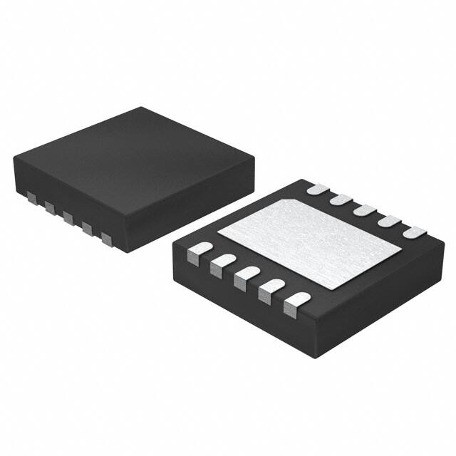
QFN-10 (3mmx3mm)
SOIC-8 EP
ABSOLUTE MAXIMUM RATINGS (1)
Thermal Resistance
Supply Voltage (VIN) ………… ..... -0.3V to +80V
Switch Voltage (VSW) …… …….-0.3V to VIN + 1V
BST to SW…………………………-0.3V to +6.0V
All Other Pins……………… . ……-0.3V to +6.0V
EN Sink Current ………………..........……150μA
(2)
Continuous Power Dissipation (TA = +25°C)
QFN-10 (3mmx3mm)…………………….......2.5W
SOIC-8 EP ……..…………………..…………2.6W
Junction Temperature………… .. …………150C
Lead Temperature ………… ...... …………260C
Storage Temperature…………. -65°C to +150C
QFN-10 (3mmx3mm) …………50……12…C/W
SOIC-8 EP ……..………………48……12…C/W
Recommended Operating Conditions
(3)
Supply Voltage VIN ………… ........... 4.5V to 75V
Output Voltage VOUT
.. …………1V to 0.9xVIN
Operating Junction Temp. (TJ). -40°C to +125°C
(4)
θJA
θJC
Notes:
1) Exceeding these ratings may damage the device.
2) The maximum allowable power dissipation is a function of the
maximum junction temperature TJ (MAX), the junction-toambient thermal resistance θJA, and the ambient temperature
TA. The maximum allowable continuous power dissipation at
any ambient temperature is calculated by PD (MAX) = (TJ
(MAX)-TA)/θJA. Exceeding the maximum allowable power
dissipation will cause excessive die temperature, and the
regulator will go into thermal shutdown. Internal thermal
shutdown circuitry protects the device from permanent
damage.
3) The device is not guaranteed to function outside of its
operating conditions.
4) Measured on JESD51-7, 4-layer PCB.
MPQ4569 Rev. 1.02
www.MonolithicPower.com
5/25/2016
MPS Proprietary Information. Patent Protected. Unauthorized Photocopy and Duplication Prohibited.
© 2016 MPS. All Rights Reserved.
3
�MPQ4569―75V, 0.3A, SYNCHRONOUS STEP-DOWN CONVERTER
ELECTRICAL CHARACTERISTICS
VIN = 24V, VEN = 2V, TJ = - 40C to +125C, unless otherwise noted. Typical values are at
TJ=+25°C.
Parameter
Condition
Supply Quiescent Current
Shutdown Supply Current
VIN UVLO Rising Threshold
No load, VFB=1.2V
VEN < 0.3V
VIN UVLO Falling Threshold
VIN UVLO Hysteresis
Feedback Voltage
Feedback Current
(5)
VREF Pin Voltage
Upper Switch On Resistance
Lower Switch On Resistance
Lower Switch Leakage
Min
Typ
Max
Units
3.9
20
2.2
4.2
30
5
4.4
μA
μA
V
3.75
0.45
1
3.95
1.01
1.02
50
1.035
V
V
V
V
nA
V
0.45
1.5
2.5
0.625
0.9
1
Ω
Ω
Ω
Ω
μA
720
810
mA
3.45
VIN=4.5V to 75V, TJ=25 °C
VIN=4.5V to 75V,
VFB=1.2V
VIN=4.5V to 75V, IREF=100μA
0.99
0.98
-50
0.965
VBST-VSW =5V, TJ=25 °C
VBST-VSW =5V,
VBIAS=5V, TJ=25 °C
VBIAS=5V
VEN = 0V, VSW = 75V
0.9
0.7
0.275
0.2
Peak Current Limit
630
(6)
Minimum Switch On Time
Enable Rising Threshold
Enable Falling Threshold
Enable Threshold Hysteresis
Enable Current
Soft Start Current
(5)
POK Upper Trip Threshold
(5)
POK Lower Trip Threshold
(5)
POK Threshold Hysteresis
(5)
POK Deglitch Timer
(5)
POK Output Voltage Low
FB OVP Rising Threshold
1.25
1.152
VEN=2.4V
4
FB respect to the nominal value
FB respect to the nominal value
FB respect to the nominal value
1.2
120
1.55
1.2
0.35
0.8
5.5
1.85
1.248
90
85
5
40
ISINK = 1mA
FB OVP Hysteresis
Thermal Shutdown
86
81
2
1
(6)
Thermal Shutdown
(6)
Hysteresis
1.05
7
94
89
0.4
1.1
ns
V
V
V
μA
μA
%
%
%
μs
V
V
50
mV
175
C
20
C
Notes:
5) QFN package only.
6) Derived from bench characterization. Not tested in production.
MPQ4569 Rev. 1.02
www.MonolithicPower.com
5/25/2016
MPS Proprietary Information. Patent Protected. Unauthorized Photocopy and Duplication Prohibited.
© 2016 MPS. All Rights Reserved.
4
�MPQ4569―75V, 0.3A, SYNCHRONOUS STEP-DOWN CONVERTER
PIN FUNCTIONS
Pin #
QFN-10
(3mmx3mm)
Pin #
SOIC-8
EP
Name
Description
1
1
GND
Ground. Connected the output capacitor as close as possible to avoid
high-current switch paths.
2
2
IN
Input Supply. Requires a decoupling capacitor to ground to reduce
switching spikes.
3
3
EN
Enable Input. Pull this pin below the low threshold to shut the chip down.
Pull it above the high threshold enables the chip. Float this pin to shut the
chip down.
4
No
Bonding
VREF
5
4
FB
6
5
SS
7
No
Bonding
POK
8
6
BIAS
9
7
BST
10
8
SW
Reference Voltage Output, for QFN-10 (3mmx3mm) package only.
Feedback Connected to the tap of an external resistive divider between
the output and GND. Sets the regulation voltage when compared to the
internal 1V reference.
Soft-Start Control Input. Connect a capacitor from SS to GND to set the
soft-start period.
Open Drain Power Good Output. “HIGH” output indicates VOUT is higher
than 90% of reference. POK is pulled down in shutdown, for QFN-10
(3mmx3mm) package only
Controller Bias Input. Supplies current to the internal circuit when
VBIAS>2.9V.
Bootstrap. Positive power supply for the internal floating high-side
MOSFET driver. Connect a bypass capacitor between this pin and SW
pin.
Switch Node.
MPQ4569 Rev. 1.02
www.MonolithicPower.com
5/25/2016
MPS Proprietary Information. Patent Protected. Unauthorized Photocopy and Duplication Prohibited.
© 2016 MPS. All Rights Reserved.
5
�MPQ4569―75V, 0.3A, SYNCHRONOUS STEP-DOWN CONVERTER
TYPICAL CHARACTERISTICS
VIN=12V, unless otherwise noted.
MPQ4569 Rev. 1.02
www.MonolithicPower.com
5/25/2016
MPS Proprietary Information. Patent Protected. Unauthorized Photocopy and Duplication Prohibited.
© 2016 MPS. All Rights Reserved.
6
�MPQ4569―75V, 0.3A, SYNCHRONOUS STEP-DOWN CONVERTER
TYPICAL PERFORMANCE CHARACTERISTICS
VIN = 12V, VOUT = 3.3V, L = 33µH, COUT=2x22μF, TA = +25°C, unless otherwise noted.
MPQ4569 Rev. 1.02
www.MonolithicPower.com
5/25/2016
MPS Proprietary Information. Patent Protected. Unauthorized Photocopy and Duplication Prohibited.
© 2016 MPS. All Rights Reserved.
7
�MPQ4569―75V, 0.3A, SYNCHRONOUS STEP-DOWN CONVERTER
TYPICAL PERFORMANCE CHARACTERISTICS (continued)
VIN = 12V, VOUT = 3.3V, L = 33µH, COUT=2x22μF, TA = +25°C, unless otherwise noted.
MPQ4569 Rev. 1.02
www.MonolithicPower.com
5/25/2016
MPS Proprietary Information. Patent Protected. Unauthorized Photocopy and Duplication Prohibited.
© 2016 MPS. All Rights Reserved.
8
�MPQ4569―75V, 0.3A, SYNCHRONOUS STEP-DOWN CONVERTER
FUNCTIONAL BLOCK DIAGRAM
VIN
BIAS
BST
REGULATOR
REF
VREF
EN
ICOMP
EN Control
+
3M
ILIMIT
POK
POK
+
+
SS
-
S
RS
R
COMP
SS
-
SW
ZCD
FB
GND
Figure 1 - Functional Block Diagram
MPQ4569 Rev. 1.02
www.MonolithicPower.com
5/25/2016
MPS Proprietary Information. Patent Protected. Unauthorized Photocopy and Duplication Prohibited.
© 2016 MPS. All Rights Reserved.
9
�MPQ4569―75V, 0.3A, SYNCHRONOUS STEP-DOWN CONVERTER
OPERATION
The MPQ4569 is a 75V, 0.3A, synchronous,
step-down switching regulator with integrated
high-side and low-side high-voltage power
MOSFETs (HS_FET and LS_FET, respectively).
It provides a highly-efficient, 0.3A output. It
features a wide input voltage range, external softstart control, and precision current limit. Its very
low operational quiescent current makes it
suitable for battery-powered applications.
Control Scheme
The ILIM comparator, FB comparator and zero
current detector (ZCD) block control the PWM. If
VFB is below the 1V reference and the inductor
current drops to zero, HS_FET turns on and the
ILIM comparator starts to sense the HS_FET
current: When the HS_FET current reaches the
limit, the HS_FET turns off and LS_FET turns on
together with the ZCD block. Meanwhile, the ILIM
comparator is turned off to reduce the quiescent
current. The LS_FET turns off together with ZCD
block after the inductor current drops to zero. If
VFB is less than the 1V reference at this time, the
HS_FET turns on at once and commences
another cycle. If VFB is still higher than 1V
reference, HS_FET would not turn on till VFB
drops below 1V.
VFB
VREF
VSW
IL
Ipeak
Io
Io increase
Internal Regulator and BIAS
The 2.6V internal regulator powers most of the
internal circuitry. This regulator takes VIN and
operates in the full VIN range. When VIN is greater
than 3.0V, the output of the regulator is in full
regulation. Lower values of VIN result in lower
output voltages. When VBIAS>2.9V, the bias
supply overrides the input voltage and supplies
power to the internal regulator. When VBIAS>4.5V,
it can power LS_FET driver furthermore. Using
BIAS to power internal regulator can improve the
efficiency. It is recommended to connect BIAS to
the regulated output voltage when it is in the
range of 2.9V to 5.5V. When output voltage is out
of above range, an external supply that is >2.9V
or even better >4.5V can be used to power BIAS.
Enable Control
The MPQ4569 has a dedicated enable-control
pin, EN: when VIN goes high, the EN pin enables
and disables the chip. This is HIGH logic. Its
trailing threshold is a consistent 1.2V. Its rising
threshold is about 350mV higher. When floating,
EN pin is internally pulled down to GND to
disable the chip.
When EN = 0V, the chip goes into the lowest
shutdown-current mode. When EN is higher than
zero but lower than its rising threshold, the chip
remains in shutdown mode with a slightly larger
shutdown current.
Internally a zener diode is connected from EN pin
to GND pin. The typical clamping voltage of the
zener diode is 6.5V. So VIN can be connected to
EN through a high ohm resistor if the system
doesn't have another logic input acting as enable
signal. The resistor needs to be designed to limit
the EN pin sink current less than 150μA. Just
note that there is an internal 3M resistor from EN
to GND, so the external pull up resistor should be
smaller than
[VIN (MIN) - 1.55V] 3M
to make sure
1.55V
the part can EN on at the lowest operation VIN.
Figure2 - Control Scheme
MPQ4569 Rev. 1.02
www.MonolithicPower.com
5/25/2016
MPS Proprietary Information. Patent Protected. Unauthorized Photocopy and Duplication Prohibited.
© 2016 MPS. All Rights Reserved.
10
�MPQ4569―75V, 0.3A, SYNCHRONOUS STEP-DOWN CONVERTER
Under-Voltage Lockout
VIN under voltage lockout (UVLO) protects the
chip from operating below the operational supply
voltage range. The UVLO-rising threshold is
about 4.2V while its trailing threshold is about
3.75V.
Soft-start
Reference-type soft-start prevents the converter
output voltage from overshooting during startup.
When the chip starts, the internal circuitry
generates a constant current to charge external
SS capacitor. The soft-start (SS) voltage slowly
ramps up from 0V at a slow pace set by the softstart time. When VSS is less than the VREF, VSS
overrides VREF so the FB comparator uses VSS
instead of VREF as the reference. When VSS is
higher than VREF, VREF resumes control.
VSS is also associated with VFB. Though VSS can
be much smaller than VFB, it can only barely
exceed VFB. If somehow VFB drops, VSS tracks
VFB. This function prevents output voltage
overshoot in short-circuit recovery -- when the
short circuit is removed, the SS ramps up as if it
is a fresh soft-start process.
Thermal Shutdown
Thermal shutdown prevents the chip from
thermally running away. When the silicon die
temperature exceeds its upper threshold, the
thermal shutdown feature shuts down the whole
chip. When the temperature falls below its lower
threshold, the chip resumes function.
Floating Driver and Bootstrap Charging
The external bootstrap capacitor powers the
floating HS_FET driver. This floating driver has
its own UVLO protection, with a rising threshold
of about 2.4V with a hysteresis of about 300mV.
During this UVLO, the SS voltage resets to zero.
When the UVLO is disabled, the regulator follows
the soft-start process.
The dedicated internal bootstrap regulator
charges and regulates the bootstrap capacitor to
about 5V. When the voltage difference between
BST and SW falls below its working parameters,
a PMOS pass transistor connected from VIN to
BST turns on to charge the bootstrap capacitor.
The current path is from VIN to BST and then to
SW. The external circuit must have enough
voltage headroom to accommodate charging.
As long as VIN is sufficiently higher than SW, the
bootstrap capacitor can charge. When the
HS_FET is ON, VIN is about equal to SW so the
bootstrap capacitor cannot charge. The best
charging period occurs when the LS_FET is on
so that VIN - VSW is at its largest. When there is
no current in the inductor, VSW equals VOUT so the
difference between VIN and VOUT can charge the
bootstrap capacitor.
If the internal circuit does not have sufficient
voltage and time to charge the bootstrap
capacitor, extra external circuitry can be used to
ensure the bootstrap voltage in normal operation
region.
Startup and Shutdown
If both VIN and VEN are higher than their
appropriate thresholds, the chip starts operating.
The reference block starts first, generating stable
reference voltage and currents, and then enables
the internal regulator. The regulator provides
stable supply for the rest device.
While the internal supply rail is high, an internal
timer holds the power MOSFET off for about
50µsec to blank startup glitches. When the softstart block is enabled, it first holds its SS output
low and then slowly ramps up.
Three events shut down the chip: VEN low, VIN
low, and junction temperature triggers the
thermal shutdown threshold. For shutdown, the
signaling path is blocked first to avoid any fault
triggering. Internal supply rail is pulled down then.
The floating driver is not subject to this shutdown
command, but its charging path is disabled.
Power OK (POK)
POK is an open drain power good output. “HIGH”
output indicates VOUT is higher than 90% of its
nominal value. POK is pulled down in shutdown
mode.
Reference Voltage Output (VREF)
VREF pin output 1V reference voltage. It has up
to 500uA source current capability.
MPQ4569 Rev. 1.02
www.MonolithicPower.com
5/25/2016
MPS Proprietary Information. Patent Protected. Unauthorized Photocopy and Duplication Prohibited.
© 2016 MPS. All Rights Reserved.
11
�MPQ4569―75V, 0.3A, SYNCHRONOUS STEP-DOWN CONVERTER
APPLICATION INFORMATION
To get the desired output voltage, divider resistor
Selecting the Inductor
VOUT
As the Ipeak is fixed, for given input voltage and
output voltage, the inductor value can be
determined by the following formula:
R4
L
VOUT VIN - VOUT
VIN Ipeak fs
Where fs is the switching frequency at the
maximal output current.
Larger inductor value results in lower switching
frequency, as well as higher efficiency. However,
the larger value inductor will have a larger
physical size, higher series resistance, and/or
lower saturation current as well as the slow load
transient dynamic performance. There is also a
lower limit of the inductor value, which is
determined by the minimum on time. In order to
keep the inductor working under control, the
inductor value should be chosen higher than
Lmin that is derived from below formula:
L MIN
VIN (MAX ) t ON(MIN)
Ipeak
Where VIN(MAX) is the max value of input voltage.
tON(MIN) is the 120ns minimum switch on time.
Switching Frequency
Switching frequency can be estimated by below
equation.
fs
2 Io VOUT VIN - VOUT
2
Ipeak
VIN L
Larger inductor can get lower fs. And fs
increases as Io increasing. When Io increases to
its maximal value Ipeak/2, fs also reaches its
highest value and can be derived by:
fs(max)
VOUT VIN - VOUT
Ipeak VIN L
Setting the Output Voltage
The output voltage is set using a resistive voltage
divider from the output voltage to FB pin. As
shown in figure 3.
FB
R5
Figure 3 – Adjustable VOUT by divider resistors
can be chosen through below formula:
R4 VOUT
-1
R5 VREF
Where VREF is the FB reference voltage 1V.
The current flows into divider resistor would
increase the supply current, especially at no load
and light load condition. The Vin supply current
caused by the feedback resistors can be
calculated from:
IIN_FB
VOUT
V
1
OUT
R4 R5 VIN η
Where η is the efficiency of the regulator.
To reduce this current, resistors in the megohm
range are recommended. The recommended
value of the feedback resistors are shown in
Table 1.
Table 1—Resistor Selection for Common
Output Voltages
VOUT (V)
R4 (kΩ)
R5 (kΩ)
3.3
5
1200
1200
523
300
Under Voltage Lock Out Point Setting
MPQ4569 has internal fixed under voltage lock
out (UVLO) threshold: rising threshold is about
4.2V while trailing threshold is about 3.75V.
External resistor divider between EN and VIN as
shown in Figure 4 can be used to get higher
equivalent UVLO threshold.
VIN
IN
R1
R2
EN
3M
Figure 4 – Adjustable UVLO using EN pin
MPQ4569 Rev. 1.02
www.MonolithicPower.com
5/25/2016
MPS Proprietary Information. Patent Protected. Unauthorized Photocopy and Duplication Prohibited.
© 2016 MPS. All Rights Reserved.
12
�MPQ4569―75V, 0.3A, SYNCHRONOUS STEP-DOWN CONVERTER
The UVLO threshold can be computed from
below two equations.
R1
) ENTH_Rising
3M//R2
R1
UVLO TH_Falling (1
) ENTH_Falling
3M//R2
UVLO TH_Rising (1
5) For better thermal performance and long-term
reliability consideration, VIN, SW and GND
should be connected to a large copper area
respectively to cool the chip.
Soft Start Capacitor
The soft start time is the duration when SS is
charged from 0 to FB reference voltage 1V by an
internal 5μA current source. So the capacitor at
SS pin can be chosen according to below
formula:
CSS 5 t SS (μF)
Feedforward Capacitor
As described above that the PWM control
scheme of MPQ4569 is very special and the
HS_FET turns on when FB drops lower than
reference voltage. This brings good load
transient performance. However, this also makes
the HS_FET turn on moment is very sensitive to
the FB voltage. Once there is noise on FB, the
moment HS_FET turns on is easy to be affected,
and then Fsw jitter would occur. The Fsw jitter is
easy to happen especially when Vo ripple is very
small. To improve the jitter performance, a small
feedforward capacitor between Vo and FB can
be used and typical 39pF is recommended.
Top Layer
PCB Layout
PCB layout is very important to achieve stable
operation. Please follow below guidelines and
use Figure 5 as reference.
1) Keep the path of switching current short and
minimize the loop area formed by input
capacitor, high-side, low-side MOSFET and
output capacitor.
2) Bypass ceramic capacitors should be as close
as possible to the VIN pin.
3) Make sure that all feedback connections are
short and direct. Place the feedback resistors
as close to the chip as possible.
4) Keep SW away from sensitive analog areas
such as FB.
Bottom Layer
1) Layout Reference of QFN-10 Package(7)
MPQ4569 Rev. 1.02
www.MonolithicPower.com
5/25/2016
MPS Proprietary Information. Patent Protected. Unauthorized Photocopy and Duplication Prohibited.
© 2016 MPS. All Rights Reserved.
13
�MPQ4569―75V, 0.3A, SYNCHRONOUS STEP-DOWN CONVERTER
Top Layer
Bottom Layer
2) Layout Reference of SOIC-8 EP Package(8)
Figure 5 – Layout Reference
Notes:
7) Take Figure 6 as schematic
8) Take Figure 7 as schematic
MPQ4569 Rev. 1.02
www.MonolithicPower.com
5/25/2016
MPS Proprietary Information. Patent Protected. Unauthorized Photocopy and Duplication Prohibited.
© 2016 MPS. All Rights Reserved.
14
�MPQ4569―75V, 0.3A, SYNCHRONOUS STEP-DOWN CONVERTER
TYPICAL APPLICATION CIRCUITS
C3
0.1uF
U1
4.5V-75V
2
VIN
R1
1M
C1A
10uF
100V
C1B
0.1uF
100V
GND
3
VIN
L1
33uH
9
BST
SW
3.3V/300mA
10
VOUT
C2
22uF
16V
MPQ4569GQ
EN
GND
BIAS
R3
8
10
R2
NS
C4
0.1uF
4
VREF
FB
R4 1.2M
5
C7
1uF
C5
R5
523K
39pF
R6
100K
6
SS
GND
POK
7
1
C6
10nF
Figure 6 – 3.3V Output Typical Application Circuit of QFN-10 Package
C3
0.1uF
U1
4.5V-75V
2
VIN
R1
1M
C1A
10uF
100V
C1B
0.1uF
100V
GND
3
VIN
L1
33uH
7
BST
SW
3.3V/300mA
8
VOUT
C2
22uF
16V
MPQ4569GN
EN
BIAS
GND
R3
6
10
R2
NS
C4
0.1uF
5
C6
10nF
FB
SS
GND
1
R4 1.2M
4
R5
523K
C5
39pF
Figure 7 – 3.3V Output Typical Application Circuit of SOIC-8 EP Package
MPQ4569 Rev. 1.02
www.MonolithicPower.com
5/25/2016
MPS Proprietary Information. Patent Protected. Unauthorized Photocopy and Duplication Prohibited.
© 2016 MPS. All Rights Reserved.
15
�MPQ4569―75V, 0.3A, SYNCHRONOUS STEP-DOWN CONVERTER
PACKAGE INFORMATION
QFN-10 (3mmx3mm)
MPQ4569 Rev. 1.02
www.MonolithicPower.com
5/25/2016
MPS Proprietary Information. Patent Protected. Unauthorized Photocopy and Duplication Prohibited.
© 2016 MPS. All Rights Reserved.
16
�MPQ4569―75V, 0.3A, SYNCHRONOUS STEP-DOWN CONVERTER
SOIC-8 EP
NOTICE: The information in this document is subject to change without notice. Please contact MPS for current specifications.
Users should warrant and guarantee that third party Intellectual Property rights are not infringed upon when integrating MPS
products into any application. MPS will not assume any legal responsibility for any said applications.
MPQ4569 Rev. 1.02
www.MonolithicPower.com
5/25/2016
MPS Proprietary Information. Patent Protected. Unauthorized Photocopy and Duplication Prohibited.
© 2016 MPS. All Rights Reserved.
17
�


 工商网监
湘ICP备2023018690号
工商网监
湘ICP备2023018690号
