1N4001, 1N4002, 1N4003,
1N4004, 1N4005, 1N4006,
1N4007
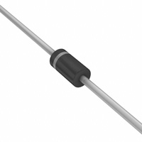
Axial-Lead Glass
Passivated Standard
Recovery Rectifiers
www.onsemi.com
This data sheet provides information on subminiature size, axial
lead mounted rectifiers for general−purpose low−power applications.
Features
• Shipped in Plastic Bags, 1000 per bag
• Available Tape and Reeled, 5000 per reel, by adding a “RL” suffix to
•
•
LEAD MOUNTED RECTIFIERS
50−1000 VOLTS
DIFFUSED JUNCTION
the part number
Available in Fan−Fold Packaging, 3000 per box, by adding a “FF”
suffix to the part number
Pb−Free Packages are Available
Mechanical Characteristics
• Case: Epoxy, Molded
• Weight: 0.4 gram (approximately)
• Finish: All External Surfaces Corrosion Resistant and Terminal
CASE 59−10
AXIAL LEAD
PLASTIC
Leads are Readily Solderable
• Lead and Mounting Surface Temperature for Soldering Purposes:
•
260°C Max. for 10 Seconds, 1/16 in. from case
Polarity: Cathode Indicated by Polarity Band
MARKING DIAGRAM
*For additional information on our Pb−Free strategy and soldering details, please
download the ON Semiconductor Soldering and Mounting Techniques
Reference Manual, SOLDERRM/D.
A
1N400x
YYWWG
G
A
= Assembly Location
1N400x = Device Number
x
= 1, 2, 3, 4, 5, 6 or 7
YY
= Year
WW
= Work Week
G
= Pb−Free Package
(Note: Microdot may be in either location)
ORDERING INFORMATION
See detailed ordering and shipping information on page 5 of
this data sheet.
© Semiconductor Components Industries, LLC, 2012
June, 2018 − Rev. 14
1
Publication Order Number:
1N4001/D
�1N4001, 1N4002, 1N4003, 1N4004, 1N4005, 1N4006, 1N4007
MAXIMUM RATINGS
Symbol
1N4001
1N4002
1N4003
1N4004
1N4005
1N4006
1N4007
Unit
†Peak Repetitive Reverse Voltage
Working Peak Reverse Voltage
DC Blocking Voltage
Rating
VRRM
VRWM
VR
50
100
200
400
600
800
1000
V
†Non−Repetitive Peak Reverse Voltage
(halfwave, single phase, 60 Hz)
VRSM
60
120
240
480
720
1000
1200
V
VR(RMS)
35
70
140
280
420
560
700
V
†RMS Reverse Voltage
†Average Rectified Forward Current
(single phase, resistive load,
60 Hz, TA = 75°C)
IO
1.0
A
†Non−Repetitive Peak Surge Current
(surge applied at rated load conditions)
IFSM
30 (for 1 cycle)
A
Operating and Storage Junction
Temperature Range
TJ
Tstg
−65 to +175
°C
Stresses exceeding those listed in the Maximum Ratings table may damage the device. If any of these limits are exceeded, device functionality
should not be assumed, damage may occur and reliability may be affected.
†Indicates JEDEC Registered Data
THERMAL CHARACTERISTICS
Rating
Maximum Thermal Resistance, Junction−to−Ambient
Symbol
Max
Unit
RqJA
Note 1
°C/W
ELECTRICAL CHARACTERISTICS†
Rating
Maximum Instantaneous Forward Voltage Drop, (iF = 1.0 Amp, TJ = 25°C)
Maximum Full−Cycle Average Forward Voltage Drop, (IO = 1.0 Amp, TL = 75°C, 1 inch leads)
Maximum Reverse Current (rated DC voltage)
(TJ = 25°C)
(TJ = 100°C)
Symbol
Typ
Max
Unit
vF
0.93
1.1
V
VF(AV)
−
0.8
V
0.05
1.0
10
50
−
30
IR
Maximum Full−Cycle Average Reverse Current, (IO = 1.0 Amp, TL = 75°C, 1 inch leads)
IR(AV)
mA
mA
Product parametric performance is indicated in the Electrical Characteristics for the listed test conditions, unless otherwise noted. Product
performance may not be indicated by the Electrical Characteristics if operated under different conditions.
†Indicates JEDEC Registered Data
www.onsemi.com
2
�1N4001, 1N4002, 1N4003, 1N4004, 1N4005, 1N4006, 1N4007
IR, REVERSE CURRENT (A)
1.0E−04
TC = 100°C
1
1.0E−05
TC = 150°C
1.0E−06
TC = 100°C
1.0E−07
TC = 150°C
0.1
0.5
1.0E−08
TC = 25°C
TC = 25°C
0.6
0.7
0.8
0.9
1.1
1
1.2
1.0E−09
0
100 200
VF, INSTANTANEOUS FORWARD VOLTAGE (V)
300 400 500
Figure 2. Typical Reverse Current
100
TJ = 25°C
10
1
0
20
40
600 700 800 900 1000
VR, REVERSE VOLTAGE (V)
Figure 1. Typical Forward Voltage
C, CAPACITANCE (pF)
IF, FORWARD CURRENT (A)
10
60
80
100
120 140 160 180 200
VR, REVERSE VOLTAGE (V)
Figure 3. Typical Capacitance
www.onsemi.com
3
�1N4001, 1N4002, 1N4003, 1N4004, 1N4005, 1N4006, 1N4007
NOTE 1. − AMBIENT MOUNTING DATA
Data shown for thermal resistance, junction−to−ambient
(RqJA) for the mountings shown is to be used as typical
guideline values for preliminary engineering or in case the
tie point temperature cannot be measured.
TYPICAL VALUES FOR RqJA IN STILL AIR
Mounting
Method
1
2
RqJA
Lead Length, L
1/4
1/2
1/8
52
65
72
67
80
87
Units
°C/W
°C/W
50
°C/W
3
MOUNTING METHOD 1
L
L
ÉÉÉÉÉÉÉÉÉÉÉ
ÉÉÉÉÉÉÉÉÉÉÉ
MOUNTING METHOD 2
ÉÉÉÉÉÉÉÉÉÉÉÉ
ÉÉÉÉÉÉÉÉÉÉÉÉ
L
L
Vector Pin Mounting
ÉÉ
ÉÉ
ÉÉ
ÉÉ
ÉÉ
ÉÉ
ÉÉ
MOUNTING METHOD 3
L = 3/8 ″
Board Ground Plane
P.C. Board with
1−1/2 ″ X 1−1/2 ″ Copper Surface
www.onsemi.com
4
�1N4001, 1N4002, 1N4003, 1N4004, 1N4005, 1N4006, 1N4007
ORDERING INFORMATION
Package
Shipping†
1N4001
Axial Lead*
1000 Units/Bag
1N4001G
Axial Lead*
(Pb−Free)
1000 Units/Bag
1N4001FF
Axial Lead*
3000 Units/Box
1N4001FFG
Axial Lead*
(Pb−Free)
3000 Units/Box
1N4001RL
Axial Lead*
5000/Tape & Reel
1N4001RLG
Axial Lead*
(Pb−Free)
5000/Tape & Reel
1N4002
Axial Lead*
1000 Units/Bag
1N4002G
Axial Lead*
(Pb−Free)
1000 Units/Bag
1N4002FF
Axial Lead*
3000 Units/Box
1N4002FFG
Axial Lead*
(Pb−Free)
3000 Units/Box
1N4002RL
Axial Lead*
5000/Tape & Reel
1N4002RLG
Axial Lead*
(Pb−Free)
5000/Tape & Reel
1N4003
Axial Lead*
1000 Units/Bag
1N4003G
Axial Lead*
(Pb−Free)
1000 Units/Bag
1N4003FF
Axial Lead*
3000 Units/Box
1N4003FFG
Axial Lead*
(Pb−Free)
3000 Units/Box
1N4003RL
Axial Lead*
5000/Tape & Reel
1N4003RLG
Axial Lead*
(Pb−Free)
5000/Tape & Reel
1N4004
Axial Lead*
1000 Units/Bag
1N4004G
Axial Lead*
(Pb−Free)
1000 Units/Bag
1N4004FF
Axial Lead*
3000 Units/Box
1N4004FFG
Axial Lead*
(Pb−Free)
3000 Units/Box
1N4004RL
Axial Lead*
5000/Tape & Reel
1N4004RLG
Axial Lead*
(Pb−Free)
5000/Tape & Reel
1N4005
Axial Lead*
1000 Units/Bag
1N4005G
Axial Lead*
(Pb−Free)
1000 Units/Bag
1N4005FF
Axial Lead*
3000 Units/Box
1N4005FFG
Axial Lead*
(Pb−Free)
3000 Units/Box
1N4005RL
Axial Lead*
5000/Tape & Reel
1N4005RLG
Axial Lead*
(Pb−Free)
5000/Tape & Reel
Device
†For information on tape and reel specifications, including part orientation and tape sizes, please refer to our Tape and Reel Packaging
Specifications Brochure, BRD8011/D.
*This package is inherently Pb−Free.
www.onsemi.com
5
�1N4001, 1N4002, 1N4003, 1N4004, 1N4005, 1N4006, 1N4007
ORDERING INFORMATION
Package
Shipping†
1N4006
Axial Lead*
1000 Units/Bag
1N4006G
Axial Lead*
(Pb−Free)
1000 Units/Bag
1N4006FF
Axial Lead*
3000 Units/Box
1N4006FFG
Axial Lead*
(Pb−Free)
3000 Units/Box
1N4006RL
Axial Lead*
5000/Tape & Reel
1N4006RLG
Axial Lead*
(Pb−Free)
5000/Tape & Reel
1N4007
Axial Lead*
1000 Units/Bag
1N4007G
Axial Lead*
(Pb−Free)
1000 Units/Bag
1N4007FF
Axial Lead*
3000 Units/Box
1N4007FFG
Axial Lead*
(Pb−Free)
3000 Units/Box
1N4007RL
Axial Lead*
5000/Tape & Reel
1N4007RLG
Axial Lead*
(Pb−Free)
5000/Tape & Reel
Device
†For information on tape and reel specifications, including part orientation and tape sizes, please refer to our Tape and Reel Packaging
Specifications Brochure, BRD8011/D.
*This package is inherently Pb−Free.
www.onsemi.com
6
�1N4001, 1N4002, 1N4003, 1N4004, 1N4005, 1N4006, 1N4007
PACKAGE DIMENSIONS
AXIAL LEAD
CASE 59−10
ISSUE U
B
K
NOTES:
1. DIMENSIONING AND TOLERANCING PER ANSI
Y14.5M, 1982.
2. CONTROLLING DIMENSION: INCH.
3. ALL RULES AND NOTES ASSOCIATED WITH
JEDEC DO−41 OUTLINE SHALL APPLY
4. POLARITY DENOTED BY CATHODE BAND.
5. LEAD DIAMETER NOT CONTROLLED WITHIN F
DIMENSION.
D
F
A
POLARITY INDICATOR
OPTIONAL AS NEEDED
(SEE STYLES)
DIM
A
B
D
F
K
F
K
INCHES
MIN
MAX
0.161 0.205
0.079 0.106
0.028 0.034
−−− 0.050
1.000
−−−
MILLIMETERS
MIN
MAX
4.10
5.20
2.00
2.70
0.71
0.86
−−−
1.27
25.40
−−−
ON Semiconductor and
are trademarks of Semiconductor Components Industries, LLC dba ON Semiconductor or its subsidiaries in the United States and/or other countries.
ON Semiconductor owns the rights to a number of patents, trademarks, copyrights, trade secrets, and other intellectual property. A listing of ON Semiconductor’s product/patent
coverage may be accessed at www.onsemi.com/site/pdf/Patent−Marking.pdf. ON Semiconductor reserves the right to make changes without further notice to any products herein.
ON Semiconductor makes no warranty, representation or guarantee regarding the suitability of its products for any particular purpose, nor does ON Semiconductor assume any liability
arising out of the application or use of any product or circuit, and specifically disclaims any and all liability, including without limitation special, consequential or incidental damages.
Buyer is responsible for its products and applications using ON Semiconductor products, including compliance with all laws, regulations and safety requirements or standards,
regardless of any support or applications information provided by ON Semiconductor. “Typical” parameters which may be provided in ON Semiconductor data sheets and/or
specifications can and do vary in different applications and actual performance may vary over time. All operating parameters, including “Typicals” must be validated for each customer
application by customer’s technical experts. ON Semiconductor does not convey any license under its patent rights nor the rights of others. ON Semiconductor products are not
designed, intended, or authorized for use as a critical component in life support systems or any FDA Class 3 medical devices or medical devices with a same or similar classification
in a foreign jurisdiction or any devices intended for implantation in the human body. Should Buyer purchase or use ON Semiconductor products for any such unintended or unauthorized
application, Buyer shall indemnify and hold ON Semiconductor and its officers, employees, subsidiaries, affiliates, and distributors harmless against all claims, costs, damages, and
expenses, and reasonable attorney fees arising out of, directly or indirectly, any claim of personal injury or death associated with such unintended or unauthorized use, even if such
claim alleges that ON Semiconductor was negligent regarding the design or manufacture of the part. ON Semiconductor is an Equal Opportunity/Affirmative Action Employer. This
literature is subject to all applicable copyright laws and is not for resale in any manner.
PUBLICATION ORDERING INFORMATION
LITERATURE FULFILLMENT:
Literature Distribution Center for ON Semiconductor
19521 E. 32nd Pkwy, Aurora, Colorado 80011 USA
Phone: 303−675−2175 or 800−344−3860 Toll Free USA/Canada
Fax: 303−675−2176 or 800−344−3867 Toll Free USA/Canada
Email: orderlit@onsemi.com
◊
N. American Technical Support: 800−282−9855 Toll Free
USA/Canada
Europe, Middle East and Africa Technical Support:
Phone: 421 33 790 2910
www.onsemi.com
7
ON Semiconductor Website: www.onsemi.com
Order Literature: http://www.onsemi.com/orderlit
For additional information, please contact your local
Sales Representative
1N4001/D
�


 工商网监
湘ICP备2023018690号
工商网监
湘ICP备2023018690号
