Reference Only
Spec No. JETE243A-9105D-01
P 1/9
Chip Coil (Chip Inductors) DFE2HCAH□□□□J0L REFERENCE SPECIFICATION
Murata Standard Specification【AEC-Q200】
1.Scope
This reference specification applies to DFE2HCAH□□□□J0L, Chip Coil (Chip Inductors) for Automotive
Electronic based on AEC-Q200.
2.Part Numbering
(ex)
DF
E
2H
CA
H
Product
Structure Dimension Applications
ID
(L×W)
and
Characteristics
Category
1R0
M
J
Inductance Tolerance
Dimension
0
L
Other Packaging
(T)
3.Rating
Operating Temperature Range
(Ambient temperature; Self-temperture rise is not included)
-40 to +110°C
(Product temperature; Self- temperature rise is included)
-40 to +150°C
-40 to +110°C
Storage Temperature Range.
It can be considered for use ith DCDC conerters ith a maximum oltage of 40 or less.
Customer
Part Number
Murata
Part Number
Inductance
(µH)
Tolerance
(%)
DC
Resistance
Max. (Ω)
*3 Rated Current
(A)
∗1 Based on
∗2 Based on
Inductance change Temperature rise
DFE2HCAHR33MJ0L
0.33
0.021
5.8
4.9
DFE2HCAHR47MJ0L
0.47
0.025
5.1
4.5
DFE2HCAHR68MJ0L
0.68
0.031
4.4
3.6
DFE2HCAH1R0MJ0L
1.0
0.050
3.4
3.0
DFE2HCAH1R5MJ0L
1.5
0.074
2.9
2.3
DFE2HCAH2R2MJ0L
2.2
0.101
2.5
1.9
±20
ESD
Leel
(HBM)
1k
∗1: The saturation alloable DC current alue is specified hen the decrease of the initial Inductance alue at 30%.
*2: Rated current (Based on Temperature rise) is the current alue at hich the product temperature rises to 40℃ hen
direct current is applied to the inductor ith the product mounted on our designated board.
∗3: alue defined hen DC current flos and Rated Current (Based on Inductance change) or hen DC current flos
and Rated Current (Based on Temperature rise) hicheer is smaller.
4. Testing Conditions (Standard atmospheric conditions)
Temperature : Ordinary Temperature (5 to 35℃)
Humidity
: Ordinary Humidity (45 to 85% (RH))
Temperature
Humidity
Atmospheric Pressure
: 20 ± 2°C
: 65±5% (RH)
: 86 to 106 kPa
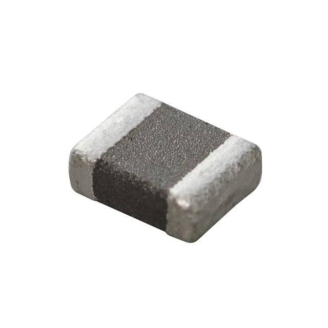
5.Appearance and Dimensions
0.6±0.3
■Unit Mass (Typical alue)
2.0±0.2
※no marking
2.5±0.2
1.2max.
(in mm)
MURATA MFG.CO., LTD
0.0324g
�Reference Only
Spec No. JETE243A-9105D-01
P 2/9
6. Electrical Performance
No.
6.1
No.
Inductance
6.2
DC Resistance
6.3
Withstand
oltage
Item
Meet item 3
Inductance:Meet item 3
Specification
Measuring Equipment:
KEYSIGHT 4284A or equialent (0.5)
Measuring Frequency: 1MHz
Measuring Equipment: Resistance Hitester 3541(HIOKI) or
equialent
machine: impulse testing machine
applied oltage: 60-70
7. Q200 Requirement
AEC-Q200 Rev.D issued June 1. 2010
AEC-Q200
Stress
No.
3 High
Temperature
Exposure
Test Method
1000±12h at 150±2 deg C
Set for 24±2hours
at room temperature,
then measured.
4
Temperature Cycling
1000cycles
-40 deg C for 30 min and 150 deg C for
30 min ith the transit period of
2min or less
Measured ithin 24±2hours
at room temperature.
7
Biased Humidity
1000±12h at 85±2 deg C, 85%RH
Measured ithin 24±2hours
at room temperature.
8
Operational Life
Apply 110±2 deg C 1000±12h
Measured ithin 24±2h
at room temperature.
10 Physical Dimension
Measures using digital slide calipers and
an optical microscope.
MURATA MFG.CO., LTD
Murata Specification / Deiation
Meet Table A after testing.
Table A
Appearance
Inductance
Change from
an initial alue
No damage
ithin ± 10%
According to specification
�Reference Only
Spec No. JETE243A-9105D-01
P 3/9
AEC-Q200
Stress
No.
13
Mechanical Shock
14
ibration
15
Resistance
to Soldering Heat
17
ESD
18
Solderability
21
Board Flex
22
Terminal Strength
Test Method
Peak acceleration:
981 m/s2 (≒100G)
Duration of pulse: 6 ms
3 times in each of 6(±X, ±Y, ±Z) axes
Murata Specification / Deiation
Meet Table A after testing.
Three successie shock shall be applied in
the perpendicular direction of each surface
of the specimen.
5G for 20 min,
for 4 hours in each of 3(X, Y, Z) axes
Test from 10-2000Hz
Pre-heating:150 to 180 deg C / 90±30sec
Reflo soldering method
aboe 220 deg C, 60±30 sec
Temperature condition
aboe 255 deg C, aboe 30sec
Peak:aboe 260deg C
The specimen shall be subjected to the
reflo process under the aboe condition 3
times. Test board shall be 1.6 mm thick.
Base material shall be glass epoxy resin.
The specimen shall be stored at standard
atmospheric conditions for 1 h in prior to the
measurement.
Per AEC-Q200-002
Meet Table A after testing.
1 time in each of terminals
ESD leel: Meet Item 3 (Rating)
Per J-STD-002 Condition SMD)C Method D Ne solder shall coer 90% minimum of
Electrode shall be immersed in flux at
the surface immersed.
room temperature and then shall be
immersed in solder bath after preheat.
Soldering 245±5 deg C, 5sec
Board : 40 × 100mm
Meet Table A after testing.
Thickness 1.6mm
Apply pressure gradually in the direction of
the arro at a rate of about 0.5mm/s until
bent depth reaches 2mm and hold
for 60 sec.
A static load using a R0.5 pressing tool shall
be applied to the body of the specimen in the
direction of the arro and shall be hold for
60s. Measure afte r remoing pressure.
Pressure 18N
MURATA MFG.CO., LTD
�Reference Only
Spec No. JETE243A-9105D-01
P 4/9
8. Specification of Packaging
8.1 Appearance and Dimensions of plastic tape
Unreeling direction
(in mm)
8.2 Specification of Taping
(1) Packing quantity (standard quantity)
3,000 pcs / reel
(2) Packing Method
Products shall be packed in the each embossed caity of plastic tape and sealed by coer tape.
(3) Sprocket hole
The sprocket holes are to the right as the tape is pulled toard the user.
(4) Spliced point
Plastic tape and Coer tape has no spliced point.
(5) Missing components number
Missing components number ithin 0.1 % of the number per reel or 1 pc., hicheer is greater, and
are not continuous. The specified quantity per reel is kept.
8.3 Peeling off force of coer tape
The force to peel aay the fixing seal tape 0.1~1.0N
8.4 Dimensions of Leader-tape, Trailer and Reel
There shall be leader-tape(coer tape) and trailer-tape (empty tape) as follos.
(in mm)
MURATA MFG.CO., LTD
�Reference Only
Spec No. JETE243A-9105D-01
P 5/9
8.5 Marking for reel
Customer part number, MURATA part number, Inspection number(∗1), RoHS marking(∗2), Quantity etc ・・・
∗1)
LL OOOO ×××
(1)
(2)
(3)
(1) Factory Code
(2) Date
First digit
: Year / Last digit of year
Second digit
: Month / Jan. to Sep. → 1 to 9, Oct. to Dec. → O, N, D
Third, Fourth digit : Day
(3) Serial No.
∗2) « Expression of RoHS marking »
ROHS – Y (△)
(1) (2)
(1) RoHS regulation conformity
(2) MURATA classification number
8.6 Marking for Outside package (corrugated paper box)
Customer name, Purchasing order number, Customer part number, MURATA part number, RoHS marking
(∗2) ,Quantity, etc ・・・
8.7 Specification of Outer Case
Outer Case Dimensions (mm)
Label
H
W
D
H
Standard Reel Quantity
in Outer Case (Reel)
200
185
67
5
Aboe Outer Case size is typical. It depends on a quantity of an order.
D
W
9.
Caution
9.1 Limitation of Applications
Please contact us before using our products for the applications listed belo hich require especially
high reliability for the preention of defects hich might directly cause damage to the third party's life,
body or property.
(1) Aircraft equipment
(6) Transportation equipment ( trains, ships, etc.)
(2) Aerospace equipment
(7) Traffic signal equipment
(3) Undersea equipment
(8) Disaster preention / crime preention equipment
(4) Poer plant control equipment (9) Data-processing equipment
(5) Medical equipment
(10) Applications of similar complexity and /or reliability
requirements to the applications listed in the aboe
9.2 Caution(Rating)
Do not exceed maximum rated current of the product. Thermal stress may be transmitted to the product
and short/open circuit of the product or falling off the product may be occurred.
9.3 Fail-safe
Be sure to proide an appropriate fail-safe function on your product to preent a second damage
that may be caused by the abnormal function or the failure of our product.
10. Notice
This product is designed for solder mounting.
Please consult us in adance for applying other mounting method such as conductie adhesie.
This product employs a core ith lo insulation resistance, Pay strict attention hen use it.
a) Do not make any through holes and copper pattern under the coil except a copper pattern to the electrode.
b) Design/mount any components not to contact this product.
MURATA MFG.CO., LTD
�Reference Only
Spec No. JETE243A-9105D-01
P 6/9
10.1 Land pattern designing (Reflo Soldering)
Recommended land pattern for reflo soldering is as follos:
It has been designed for Electric characteristics and solderability.
Please follo the recommended patterns. Otherise, their performance hich includes electrical performance or
solderability may be affected, or result to "position shift" in soldering process.
UNIT : mm
10.2 Flux, Solder
Flux
Solder
・Use rosin-based flux.
・Don’t use highly acidic flux ith halide content exceeding 0.2(t)% (chlorine conersion alue).
・Don’t use ater-soluble flux.
・Use Sn-3.0Ag-0.5Cu solder
・Standard thickness of solder paste : 100μm to 150μm
Other flux (except (aboe) Please contact us for details, then use.
10.3 soldering conditions (Reflo)
・Pre-heating should be in such a ay that the temperature difference beteen solder and product surface is
limited to 100°C max. Cooling into solent after soldering also should be in such a ay that the temperature
difference is limited to 100°C max.
Insufficient pre-heating may cause cracks on the product, resulting in the deterioration of product quality.
・Standard soldering profile profile is as follos.
Standard Profile
Pre-heating
150℃~180℃ 、90s±30s
Heating
Peak
temperature
Cycle of reflo
aboe 230℃ 、20s~40s
250+5/-0°C
2 times
MURATA MFG.CO., LTD
�Reference Only
Spec No. JETE243A-9105D-01
P 7/9
10.4 Solder olume
・Solder shall be used not to be exceeded the upper limits as shon belo.
・Accordingly increasing the solder olume, the mechanical stress to Chip is also increased.
Exceeding solder olume may cause the failure of mechanical or electrical performance.
Upper Limit
Recommendable
t
1/3T≦t≦T
T: thickness of electrode
10.5 Product's location
The folloing shall be considered hen designing and laying out P.C.B.’s.
(1) P.C.B. shall be designed so that products are not subject to the mechanical stress due to arping the board.
[Products direction]
a
Products shall be located in the sideays
direction to the mechanical stress.
b
〈 Poor example 〉
〈 Good example〉
(2) Components location on P.C.B. separation.
It is effectie to implement the folloing measures, to reduce stress in separating the board.
It is best to implement all of the folloing three measures; hoeer, implement as many measures
as possible to reduce stress.
Contents of Measures
Stress Leel
(1) Turn the mounting direction of the component parallel to
the board separation surface.
A >
D ∗1
(2) Add slits in the board separation part.
A
>
B
(3) Keep the mounting position of the component aay from
the board separation surface.
A >
C
Perforation
C
B
D
A
∗1 A > D is alid hen stress is added ertically to
the perforation as ith Hand Separation.
If a Cutting Disc is used, stress ill be diagonal to
the PCB, therefore A > D is inalid.
Slit
(3) Mounting Components Near Scre Holes
When a component is mounted near a scre hole,
it may be affected by the board deflection that occurs
during the tightening of the scre. Mount the component
in a position as far aay from the scre holes as possible.
Scre Hole
Recommended
10.6 Resin coating
The inductance alue may change and/or it may affect on the product's performance due to high cure-stress
of resin to be used for coating/molding products. So please pay your careful attention hen you select resin.
In prior to use, please make the reliability ealuation ith the product mounted in your application set.
10.7 Temperature rating of the circuit board and components located around
Temperature may rise up to max. 40 ℃ hen applying the rated current to the Products.
Be careful of the temperature rating of the circuit board and components located around.
10.8 Caution for use
There is possibility that the Impedance alue change due to magnetism. Don‘t use a magnet or a pair of teezers
ith magnetism hen chip coil are handled. (The tip of the teezers should be molded ith resin or pottery.)
MURATA MFG.CO., LTD
�Reference Only
Spec No. JETE243A-9105D-01
P 8/9
10.9 Magnetic Saturation
When the excessie current oer rated current is applied, the Impedance alue may change due to magnetism.
10.10 Handling of a substrate
After mounting products on a substrate, do not apply any stress to the product caused by bending or tisting
to the substrate hen cropping the substrate, inserting and remoing a connector from the substrate or
tightening scre to the substrate.
Excessie mechanical stress may cause cracking in the product.
Bending
Twisting
10.11 Storage and Handing Requirements
(1) Storage period
Use the products ithin 6 months after deliered.
Solderability should be checked if this period is exceeded.
(2) Storage conditions
・Products should be stored in the arehouse on the folloing conditions.
Temperature : -10°C to 40°C
Humidity
: 15% to 85% relatie humidity No rapid change on temperature and humidity
Don't keep products in corrosie gases such as sulfur, chlorine gas or acid, or it may cause oxidization of
electrode, resulting in poor solderability.
・Products should be stored on the palette for the preention of the influence from humidity, dust and so on.
・Products should be stored in the arehouse ithout heat shock, ibration, direct sunlight and so on.
・Products should be stored under the airtight packaged condition.
(3) Handling Condition
Care should be taken hen transporting or handling product to aoid excessie ibration or mechanical
shock.
10.12 Derating
Max. current (DC, AC) as function of product temperature (derating cure)
IOP : Loaded Current
IR : Rated Current
MURATA MFG.CO., LTD
�Reference Only
Spec No. JETE243A-9105D-01
11.
P 9/9
Note
(1)Please make sure that your product has been ealuated in ie of your specifications ith our product being
mounted to your product.
(2)You are requested not to use our product deiating from the reference specifications.
(3)The contents of this reference specification are subject to change ithout adance notice.
Please approe our product specifications or transact the approal sheet for product specifications
before ordering.
MURATA MFG.CO., LTD
�


 工商网监
湘ICP备2023018690号
工商网监
湘ICP备2023018690号
