Is Now Part of
To learn more about ON Semiconductor, please visit our website at
www.onsemi.com
�FAN431A
Programmable Shunt Regulator
Features
Description
•
•
•
•
The FAN431A is a three-terminal output adjustable regulator with thermal stability over the full operating temperature range. The output voltage can be set to any value
between VREF (approximately 2.5 V) and 36 V with two
external resistors. This device has a typical dynamic output impedance of 0.2 . Active output circuit provides a
sharp turn-on characteristic, making this device excellent
replacements for zener diodes in many applications.
Programmable Output Voltage to 36 V
Low Dynamic Output Impedance: 0.2 (Typical)
Sink Current Capability: 1.0 to 100 mA
Equivalent Full-Range Temperature Coefficient of
50 ppm/°C (Typical)
• Temperature Compensated for Operation Over Full
Rated Operating Temperature Range
• Low Output Noise Voltage
• Fast Turn-on Response
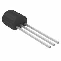
TO-92
1
1. Ref 2. Anode 3. Cathode
Ordering Information
Part Number
Operating
Temperature
Range
Output Voltage
Tolerance
Top Mark
Package
Packing
Method
FAN431AZXA
-25 to +85C
1%
FAN431A
TO-92 3L
Ammo
© 2007 Fairchild Semiconductor Corporation
FAN431A Rev. 3.4
www.fairchildsemi.com
FAN431A — Programmable Shunt Regulator
March 2015
�FAN431A — Programmable Shunt Regulator
Block Diagram
CATHODE
+
REFERENCE
2.5 Vref
ANODE
CATHODE (K)
REFERENCE (R)
ANODE(A)
Figure 1. Block Diagram
Absolute Maximum Ratings
Stresses exceeding the absolute maximum ratings may damage the device. The device may not function or be operable above the recommended operating conditions and stressing the parts to these levels is not recommended. In addition, extended exposure to stresses above the recommended operating conditions may affect device reliability. The
absolute maximum ratings are stress ratings only. Values are at TA = 25°C unless otherwise noted.
Symbol
Parameter
VKA
Cathode Voltage
IKA
Cathode current Range (Continuous)
IREF
Reference Input Current Range
R
Thermal Resistance, Junction to Ambient
Z Suffix Package
JA
(1,2)
Value
Unit
37
V
-100 to +150
mA
-0.05 to +10.00
mA
132
C/W
PD
Power Dissipation (3,4)
Z Suffix Package
940
mW
TJ
Junction Temperature
150
C
TOPR
Operating Temperature Range
-25 to +85
C
TSTG
Storage Temperature Range
-65 to +150
C
Notes:
1. Thermal resistance test board
Size: 1.6 mm x 76.2 mm x 114.3 mm (1S0P)
JEDEC Standard: JESD51-3, JESD51-7.
2. Assume no ambient airflow.
3. TJMAX = 150C, Ratings apply to ambient temperature at 25C.
4. Power dissipation calculation: PD = (TJ - TA) / R JA.
© 2007 Fairchild Semiconductor Corporation
FAN431A Rev. 3.4
www.fairchildsemi.com
2
�The Recommended Operating Conditions table defines the conditions for actual device operation. Recommended
operating conditions are specified to ensure optimal performance to the datasheet specifications. Fairchild does not
recommend exceeding them or designing to Absolute Maximum Ratings.
Symbol
Parameter
Min.
Max.
Unit
VKA
Cathode Voltage
VREF
36
V
IKA
Cathode Current
1.0
100
mA
Electrical Characteristics(5)
Values are at TA = 25°C unless otherwise noted.
Symbol
VREF
VREF/ T
Parameter
Conditions
FAN431A
Min.
Typ. Max.
Unit
Reference Input Voltage
VKA = VREF, IKA = 10 mA
2.470 2.495 2.520
V
Deviation of Reference
Input Voltage OverTemperature
VKA = VREF, IKA = 10 mA,
TMIN TA TMAX
4.5
17.0
mV
VKA = 10V - VREF
-1.0
-2.7
VKA = 36 V - 10 V
-0.5
-2.0
VREF/
VKA
Ratio of Change in
Reference Input Voltage
to Change in Cathode
Voltage
IKA = 10 mA
IREF
Reference Input Current
IKA = 10 mA, R1 = 10 k , R2 =
1.5
4.0
A
IREF/ T
Deviation of Reference
Input Current Over Full
Temperature Range
IKA = 10 mA, R1 = 10 k , R2 =
TA = Full Range
0.4
1.2
A
IKA(MIN)
Minimum Cathode
Current for Regulation
VKA = VREF
0.45
1.00
mA
IKA(OFF)
Off-Stage Cathode
Current
VKA = 36 V, VREF = 0
0.05
1.00
A
Dynamic Impedance
VKA = VREF,
IKA = 1 to 100 mA, f
0.15
0.50
ZKA
1.0 kHz
mV/V
Note:
5. TMIN = -25C, TMAX = +85C.
© 2007 Fairchild Semiconductor Corporation
FAN431A Rev. 3.4
www.fairchildsemi.com
3
FAN431A — Programmable Shunt Regulator
Recommended Operating Conditions
�FAN431
FAN431
Figure 3. Test Circuit for VKA
Figure 2. Test Circuit for VKA= VREF
VREF
FAN431
Figure 4. Test Circuit for IKA(OFF)
Typical Applications
R1
V O = 1 + ------- V
ref
R
2
V
R1
V
1
O = ref + ------R
2
R1
V O = 1 + ------- V
ref
R
2
LM7805/MC7805
FAN431
FAN431
Figure 5. Shunt Regulator
Figure 6. Output Control for ThreeTerminal Fixed Regulator
FAN431
Figure 7. High-Current Shunt
Regulator
FAN431
Figure 8. Current Limit or Current Source
Figure 9. Constant-Current Sink
© 2007 Fairchild Semiconductor Corporation
FAN431A Rev. 3.4
FAN431
www.fairchildsemi.com
4
FAN431A — Programmable Shunt Regulator
Test Circuits
�800
150
VKA = VREF
VKA = VREF
o
TA = 25 C
o
I , CATHODE CURRENT
(uA) (A)
IKA - Cathode
Current
100
50
600
IKA(MIN)
400
200
KA
0
K
I , Cathode Current
Current (mA) (mA)
IK - Cathode
T A = 25 C
-50
-100
-2
-1
0
1
2
0
-200
3
-1
0
VKA, Cathode Voltage (V)
3
Figure 11. Cathode Current vs. Cathode Voltage
0.20
3.5
0.18
Iref - Reference Input Current (A)
0.16
3.0
Iref, Reference Input Current (uA)
Ioff - Off-State Cathode Current (A)
Ioff
, Off-State Cathode Current (uA)
2
VKA - Cathode Voltage (V)
Figure 10. Cathode Current vs. Cathode Voltage
0.14
0.12
0.10
0.08
0.06
0.04
0.02
0.00
-50
1
VKA, CATHODE VOLTAGE (V)
VKA - Cathode Voltage (V)
-25
0
25
50
75
100
125
2.5
2.0
1.5
1.0
0.5
0.0
-50
150
-25
0
25
50
75
100
125
oo
TA -TAmbient
C)
, AmbientTemperature
Temperature (( C)
A
o
TAT-, Ambient
Temperature
Ambient Temperature
( C) (oC)
A
Figure 12. OFF-State Cathode Current vs.
Ambient Temperature
Figure 13. Reference Input Current vs.
Ambient Temperature
6
60
o
TA=25 C
5
40
30
20
INPUT
4
Voltage Swing (V)
50
Voltage Swing (V)
Open Loop
(dB)
Open LoopVoltage
Voltage Gain Gain
(dB)
o
TA = 25 C
IKA = 10mA
3
OUTPUT
2
10
1
0
-10
0
1k
10k
100k
1M
10M
4
8
12
16
20
Figure 15. Pulse Response
Figure 14. Frequency vs. Small Signal Voltage
Amplification
© 2007 Fairchild Semiconductor Corporation
FAN431A Rev. 3.4
0
Time (us)
Time
(s)
Frequency (Hz)
Frequency
(Hz)
www.fairchildsemi.com
5
FAN431A — Programmable Shunt Regulator
Typical Performance Characteristics
�(Continued)
5
140
A VKA = Vref
B VKA = 5.0 V @ IK = 10mA
4
o
TA = 25 C
A
100
Current (mA)
Current(mA)
IKIK,-CATHODE
CathodeCURRENT(mA)
Current (mA)
120
80
60
2
40
1
B
20
0
100p
1n
10n
100n
1?
0
0.0
10?
CCLL,-LOAD
LoadCAPACITANCE
Capacitance
0.6
0.8
1.0
1.2
1.4
1.6
1.8
2.0
VREF , Reference Input Voltage (V)
2.51
4
3
2
1
0.2
0.4
0.6
0.8
1.0
1.2
1.4
1.6
1.8
2.50
2.49
2.48
2.47
2.46
-50
2.0
Ref.-Cathode
(V)
Ref.-Cathode Voltage
Voltage(V)
Figure 18. Reference-Cathode Diode Curve
-25
0
25
50
75
TA, Ambient Temperature ( C)
o
100
125
Figure 19. Reference Input Voltage vs.
Ambient Temperature
© 2007 Fairchild Semiconductor Corporation
FAN431A Rev. 3.4
0.4
Figure 17. Anode-Reference Diode Curve
5
0
0.0
0.2
Anode-Ref.
Voltage (V)
Anode-Ref. Voltage(V)
Figure 16. Stability Boundary Conditions
Current (mA)
Current(mA)
3
www.fairchildsemi.com
6
FAN431A — Programmable Shunt Regulator
Typical Performance Characteristics
�FAN431A — Programmable Shunt Regulator
Physical Dimensions
Figure 20. 3-Lead, TO-92, Molded, 0.200 in Line Spacing Lead Form
© 2007 Fairchild Semiconductor Corporation
FAN431A Rev. 3.4
www.fairchildsemi.com
7
�
�ON Semiconductor and
are trademarks of Semiconductor Components Industries, LLC dba ON Semiconductor or its subsidiaries in the United States and/or other countries.
ON Semiconductor owns the rights to a number of patents, trademarks, copyrights, trade secrets, and other intellectual property. A listing of ON Semiconductors product/patent
coverage may be accessed at www.onsemi.com/site/pdf/Patent Marking.pdf. ON Semiconductor reserves the right to make changes without further notice to any products herein.
ON Semiconductor makes no warranty, representation or guarantee regarding the suitability of its products for any particular purpose, nor does ON Semiconductor assume any liability
arising out of the application or use of any product or circuit, and specifically disclaims any and all liability, including without limitation special, consequential or incidental damages.
Buyer is responsible for its products and applications using ON Semiconductor products, including compliance with all laws, regulations and safety requirements or standards,
regardless of any support or applications information provided by ON Semiconductor. Typical parameters which may be provided in ON Semiconductor data sheets and/or
specifications can and do vary in different applications and actual performance may vary over time. All operating parameters, including Typicals must be validated for each customer
application by customers technical experts. ON Semiconductor does not convey any license under its patent rights nor the rights of others. ON Semiconductor products are not
designed, intended, or authorized for use as a critical component in life support systems or any FDA Class 3 medical devices or medical devices with a same or similar classification
in a foreign jurisdiction or any devices intended for implantation in the human body. Should Buyer purchase or use ON Semiconductor products for any such unintended or unauthorized
application, Buyer shall indemnify and hold ON Semiconductor and its officers, employees, subsidiaries, affiliates, and distributors harmless against all claims, costs, damages, and
expenses, and reasonable attorney fees arising out of, directly or indirectly, any claim of personal injury or death associated with such unintended or unauthorized use, even if such
claim alleges that ON Semiconductor was negligent regarding the design or manufacture of the part. ON Semiconductor is an Equal Opportunity/Affirmative Action Employer. This
literature is subject to all applicable copyright laws and is not for resale in any manner.
PUBLICATION ORDERING INFORMATION
LITERATURE FULFILLMENT:
Literature Distribution Center for ON Semiconductor
19521 E. 32nd Pkwy, Aurora, Colorado 80011 USA
Phone: 303 675 2175 or 800 344 3860 Toll Free USA/Canada
Fax: 303 675 2176 or 800 344 3867 Toll Free USA/Canada
Email: orderlit@onsemi.com
Semiconductor Components Industries, LLC
N. American Technical Support: 800 282 9855 Toll Free
USA/Canada
Europe, Middle East and Africa Technical Support:
Phone: 421 33 790 2910
Japan Customer Focus Center
Phone: 81 3 5817 1050
www.onsemi.com
1
ON Semiconductor Website: www.onsemi.com
Order Literature: http://www.onsemi.com/orderlit
For additional information, please contact your local
Sales Representative
www.onsemi.com
�


 工商网监
湘ICP备2023018690号
工商网监
湘ICP备2023018690号
