LSN-16A D12 Models
www.murata-ps.com
Single Output, Non-Isolated, 12VIN, 0.75-5VOUT
16 Amp in DC/DCs SIP Packages
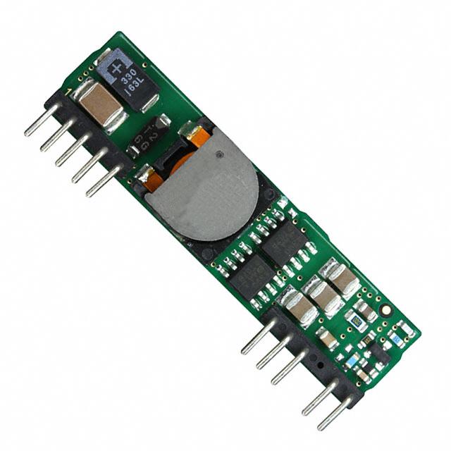
Typical Units
FEATURES
PRODUCT OVERVIEW
Step-down buck regulators for new
distributed 12V power architectures
12V input (10-14V range)
0.75/1/1.2/1.5/1.8/2.5/3.3/5VOUT @16A
Voltage-selectable "T" version
Non-isolated, fixed-frequency,
synchronous-rectifier topology
Outstanding performance:
• ±1.25% setpoint accuracy
• Efficiencies to 96% @ 16 Amps
• Noise as low as 30mVp-p
• Stable no-load operation
• Trimmable output voltage
Remote on/off control and sense
Thermal shutdown
No derating to +68°C with 200 lfm
UL/IEC/EN60950-1 certified
EMC compliant
LSN Series D12 SIP's (single-in-line packages) are ideal building blocks for emerging,
on-board power-distribution schemes in
which isolated 12V buses deliver power to
any number of non-isolated, step-down buck
regulators. LSN D12 DC/DC's accept a 12V
input (10V to 14V input range) and convert
it, with the highest efficiency in the smallest
space, to a 0.75, 1, 1.2, 1.5, 1.8, 2.5, 3.3 or
5 Volt output fully rated at 16 Amps.
LSN D12's are ideal point-of-use/load
power processors. They typically require no
external components. Their vertical-mount
packages occupy a mere 0.72 square inches
(4.6 sq. cm), and reversed pin vertical mount
allows mounting to meet competitor’s keep
out area. Horizontal-mount packages (“H”
suffix) are only 0.37 inches (9.4mm) high.
The LSN's best-in-class power density is
achieved with a fully synchronous, fixed-fre-
quency, buck topology that also delivers: high
efficiency (96% for 5VOUT models), low noise
(30 to 55mVp-p typ.), tight line/load regulation
(±0.1%/±0.25% max.), quick step response
(100μsec), stable no-load operation, and no
output reverse conduction.
The fully functional LSN’s feature output
overcurrent detection, continuous short-circuit
protection, an output-voltage trim function, a
remote on/off control pin (pull high to disable),
thermal shutdown and a sense pin. High
efficiency enables the LSN D12s to deliver
rated output currents of 16 Amps at ambient
temperatures to +68°C with 200 lfm air flow.
If your new system boards call for three or
more supply voltages, check out the economics of on-board 12V distributed power. If you
don’t need to pay for multiple isolation barriers, DATEL's non-isolated LSN D12 SIP's will
save you money.
+OUTPUT
(1,2,4)
+INPUT
(7,8)
10.5Ω
66µF
100µF
330µF
+SENSE
(3)
COMMON
(5)
COMMON
(6)
CURRENT
SENSE
VCC
ON/OFF
CONTROL
(11)
PWM
CONTROLLER
REFERENCE &
ERROR AMP
VOUT
TRIM
(10)
Typical topology is shown
Figure 1. Simplified Schematic
For full details go to
www.murata-ps.com/rohs
www.murata-ps.com/support
MDC_LSN 16A D12 Models.C01 Page 1 of 13
�LSN-16A D12 Models
Single Output, Non-Isolated, 12VIN, 0.75-5VOUT
16 Amp in DC/DCs SIP Packages
Performance Specifications and Ordering Guide ➀
ORDERING GUIDE
Output
Root Model ➆
LSN-0.75/16-D12➄
LSN-1/16-D12
LSN-1.2/16-D12
LSN-1.5/16-D12
LSN-1.8/16-D12
LSN-2/16-D12
LSN-2.5/16-D12
LSN-3.3/16-D12
LSN-5/16-D12
LSN-T/16-D12➅
VOUT
(Volts)
IOUT
(Amps)
0.75
16
16
16
16
16
16
16
16
16
16
1
1.2
1.5
1.8
2
2.5
3.3
5
0.75-5
Input
Efficiency
Load
VIN Nom.
(Volts)
Range
(Volts)
IIN ➃
(mA/A)
Min.
Typ.
Typ.
Package
(Case,
Pinout)
±0.25%
12
10-14
39/1.21
80%
82.5%
86%
B8/B8x, P59
±0.1%
±0.25%
12
10-14
39/1.45
83%
86%
86%
B8/B8x, P59
60
±0.1%
±0.25%
12
10-14
45/1.70
85%
89.5%
90%
B8/B8x, P59
45
±0.1%
±0.25%
12
10-14
54/2.09
86%
88%
91%
B8/B8x, P59
Max.
Power
(Watts)
Typ.
Max.
Line
12
45
65
±0.1%
16
45
65
19.2
45
24
30
R/N (mVp-p)
Regulation (Max.)
Full Load
½ Load
28.8
30
45
±0.1%
±0.25%
12
10-14
53/2.49
87%
90.5%
92%
B8/B8x, P59
32
30
45
±0.1%
±0.25%
12
10-14
59/2.93
88%
91%
NA
B8/B8x, P59
B8/B8x, P59
40
35
50
±0.1%
±0.25%
12
10-14
60/3.38
90.5%
92.5%
94%
52.8
40
55
±0.1%
±0.25%
12
10-14
69/4.37
92.5%
94.5%
96%
B8/B8x, P59
80
50
75
±0.1%
±0.25%
12
10-14
75/6.52
94%
96%
95.5%
B8/B8x, P59
80
55
75
±0.1%
±0.25%
12
10-14
80/7.0
95%
95.5%
96.5%
B8/B8x, P59
➀ Typical at TA = +25°C under nominal line voltage and full-load conditions, unless noted. All models
are tested and specified with external 22µF tantalum input and output capacitors. These capacitors
are necessary to accommodate our test equipment and may not be required to achieve specified
performance in your applications. See I/O Filtering and Noise Reduction.
➁ Ripple/Noise (R/N) is tested/specified over a 20MHz bandwidth and may be reduced with external
filtering. See I/O Filtering and Noise Reduction for details.
➂ These devices have no minimum-load requirements and will regulate under no-load conditions.
Regulation specifications describe the output-voltage deviation as the line voltage or load is varied
from its nominal/midpoint value to either extreme.
➃ Nominal line voltage, no-load/full-load conditions.
➄ Contact MPS for availablilty.
➅ LSN-T16-D12 efficiencies are shown at 5V out.
➆ These are incomplete model numbers. Please refer to the Part Number Structure when ordering.
PART NUMBER STRUCTURE
L SN - 1.8 / 16 - D12 H J - C
Output
Configuration:
L = Unipolar
Low Voltage
Non-Isolated SIP
Nominal Output Voltage:
0.75, 1, 1.2, 1.5, 1.8, 2.5, 3.3
or 5 Volts or "T" selectable voltage
Maximum Rated Output
Current in Amps
RoHS-6 hazardous substance compliant*
(does not claim EU RoHS exemption 7B–lead in solder)
J Suffix:
Reversed Pin
Vertical Mount
H Suffix:
Horizontal Mount
Input Voltage Range:
D12 = 10-14 Volts
(12V nominal)
* Contact MPS (DATEL) for availability.
www.murata-ps.com/support
MDC_LSN 16A D12 Models.C01 Page 2 of 13
�LSN-16A D12 Models
Single Output, Non-Isolated, 12VIN, 0.75-5VOUT
16 Amp in DC/DCs SIP Packages
MECHANICAL SPECIFICATIONS
0.37 MAX.
(9.4)
2.00
(50.8)
0.23
(5.8)
0.05
(1.27)
6 7 8 9 10 11
1 2 3 4 5
0.50
(12.7)
0.030 ± 0.002 DIA.
(0.76 ± 0.05)
0.400
(10.16)
4 EQ. SP. @
0.100 (2.54)
0.56
(14.2)
1.000
(25.40)
ISOLATING
PAD
0.030 ± 0.002 DIA.
(0.76 ± 0.05)
0.400
(10.16)
4 EQ. SP. @
0.100 (2.54)
Case B8A
Horizontal Mounting
0.50
(12.7)
0.45
(11.4)
0.23
(5.8)
MAX.
6 7 8 9 10 11
1 2 3 4 5
0.13
(3.3)
MIN.
0.360
(9.1)
0.53
(13.5)
RECOMMENDED
COPPER PAD
ON PCB (0.55 SQ. IN.)
0.17
(4.3)
0.05
(1.3)
0.500
(12.70)
5 EQ. SP. @
0.100 (2.54)
0.37 MAX.
(9.4)
2.00
(50.8)
1.000
(25.40)
0.50
(12.7)
0.05
(1.27)
0.25
(6.4)
0.11
(2.8)
0.500
(12.70)
5 EQ. SP. @
0.100 (2.54)
0.07
(1.8)
0.36
(9.2)
LAYOUT PATTERN
TOP VIEW
0.05
(1.3)
0.27
(6.9)
Case B8
Vertical Mounting
(Standard)
LAYOUT PATTERN
TOP VIEW
0.42 MAX.
(10.7)
2.00
(50.8)
Dimensions are in inches (mm shown for ref. only).
0.23
(5.8)
0.17
(4.3)
0.50
(12.7)
Third Angle Projection
6 7 8 9 10 11
1 2 3 4 5
0.030 ± 0.002 DIA.
(0.76 ± 0.05)
0.400
(10.16)
4 EQ. SP. @
0.100 (2.54)
Tolerances (unless otherwise specified):
.XX ± 0.02 (0.5)
.XXX ± 0.010 (0.25)
Angles ± 2˚
0.36
(9.1)
Components are shown for reference only.
0.05
(1.3)
1.000
(25.40)
LAYOUT PATTERN
TOP VIEW
0.05
(1.3)
0.07
(1.8)
0.13
(3.3)
0.500
(12.70)
5 EQ. SP. @
0.100 (2.54)
0.42
(10.7)
Case B8B
Reverse Pin
Vertical Mounting
(Tyco-compatible)
I/O Connections
Pin
1
2
3
4
Function P59
+Output
+Output
+Sense
+Output
Pin
5
6
7
8
Function P59
Common
Common
+Input
+Input
Pin
9
10
11
Function P59
No Pin
VOUT Trim
On/Off Control
www.murata-ps.com/support
MDC_LSN 16A D12 Models.C01 Page 3 of 13
�LSN-16A D12 Models
Single Output, Non-Isolated, 12VIN, 0.75-5VOUT
16 Amp in DC/DCs SIP Packages
Performance/Functional Specifications
Typical @ TA = +25°C under nominal line voltage and full-load conditions unless noted. ➀
Physical
Input
Input Voltage Range
10-14 Volts (12V nominal)
Input Current:
Normal Operating Conditions
Standby/Off Mode
Output Short-Circuit Condition
See Ordering Guide
5.7mA
30-60mA
Input Reflected Ripple Current ➁
30-100mAp-p
Input Filter Type
Capacitive
Start-Up Voltage
9 Volts
Overvoltage Protection
None
Reverse-Polarity Protection
None
Undervoltage Shutdown
8 Volts
No-load Input Current
50-80mA
Remote On/Off Control ➄
–Negative Logic
Outline Dimensions
See Mechanical Specifications
Pin Dimensions/Material
0.03" (0.76mm) round pins with tin plate
over copper alloy
Weight
0.3 ounces (9g)
Flammability Rating
UL94V-0
EMI Conducted and Radiated
FCC Part 15, EN55022 may require
external filter
Safety
UL/cUL 60950-1, CSA-C22.2 No.234
IEC/EN 60950-1
➀ All models are tested and specified with external 22µF input and output capacitors.
➁
ON = no connection or open
(internal pull down), 0 to +0.4V
OFF = +2.8V to +VIN or pulled high
Remote Control On/Off Current
3mA maximum
Output
➂
➃
➄
Voltage Output Accuracy (50% load)
±1.25% maximum
➅
Minimum Loading ➀
No minimum load
➆
Maximum Output Power
See Ordering Guide
VOUT x IOUT must not exceed max. power
Maximum Capacitive Loading
2,000µF (low ESR, OSCON) or
10,000µF (electrolytic) ➆
VOUT Trim Range
±10%
Sense Input Range
+10% of VOUT
Ripple/Noise (20 MHz bandwidth)
See Ordering Guide
Total Accuracy
±3% over line, load and temperature
Efficiency
See Ordering Guide
Overcurrent Detection and
Short Circuit Protection
Current-limiting Detection
Short Circuit Detection
Short Circuit Protection Method
Short Circuit Current
Short Circuit Duration
22-32 Amps, model dependent
98% of VOUT setting ➅
Hiccup with autorecovery
See Technical Notes
270-600mA (model dependent)
Continuous, output shorted to ground
Temperature Coefficient
±0.02% per °C
These capacitors are necessary to accommodate our test equipment and may not be required
to achieve specified performance in your applications. All models are stable and regulate within
spec under no-load conditions.
Input Ripple Current is tested and specified over a 5-20MHz bandwidth. Input filtering is
CIN = 200µF, CBUS = 1000µF, LBUS = 1µH.
Current limit inception is given at either cold start-up or after warm-up.
Mean Time Before Failure is calculated using the Telcordia (Bellcore) SR-332 Method 1, Case 3,
ground fixed conditions, TCASE = +25°C, full load, natural convection, +67°C max. PCB temp.
The On/Off Control (pin 11) may be driven with open-collector logic or by applying appropriate
external voltages which are referenced to Common, pins 5 and 6.
Short circuit shutdown begins when the output voltage degrades approximately 2% from the
selected setting.
Use only as much filtering to reduce noise and no more. Large, low-ESR ceramic caps may
degrade dynamic performance. Thoroughly test your system with all components installed.
Absolute Maximum Ratings
Input Voltage:
Continuous or transient
On/Off Control (Pin 11)
Input Reverse-Polarity Protection
Output Overvoltage Protection
Output Current
Storage Temperature
Lead Temperature (soldering, 10 sec.)
15Vdc maximum
+VIN
None
None
Current limited. Devices can
withstand sustained output short
circuits without damage.
–55 to +125°C
+300°C, 10 seconds maximum.
These are stress ratings. Exposure of devices to greater than any of these conditions may
adversely affect long-term reliability. Proper operation under conditions other than those
listed in the Performance/Functional Specifications Table is not implied.
Dynamic Characteristics
Transient Response
(50 to 100% load step to ±2% of Vout) 50µsec typical, 100µsec maximum
Start-Up Time On/Off to VOUT
20msec for VOUT = nominal
Switching Frequency
230-370kHz (model dependent)
Environmental
Calculated MTBF ➃
TBD Hours
Operating Temperature: (Ambient)
–40 to +85°C with derating
Storage Temperature Range
Thermal Protection/Shutdown
–55 to +125°C
115°C
Density Altitude
0 to 10,000 feet
Relative Humidity
To +85°C/85%, non-condensing
Return Current Paths
The LSN D12 SIP’s are non-isolated DC/DC converters. Their two Common
pins (pins 5 and 6) are connected to each other internally (see Figure 1). To
the extent possible (with the intent of minimizing ground loops), input return
current should be directed through pin 6 (also referred to as –Input or Input
Return), and output return current should be directed through pin 5 (also
referred to as –Output or Output Return). Any on/off control signals applied to
pin 11 (On/Off Control) should be referenced to Common (specifically pin 6).
I/O Filtering and Noise Reduction
All models in the LSN D12 Series are tested and specified with external 22μF
tantalum input and output capacitors. These capacitors are necessary to
accommodate our test equipment and may not be required to achieve desired
performance in your application. The LSN D12's are designed with high-quality,
www.murata-ps.com/support
MDC_LSN 16A D12 Models.C01 Page 4 of 13
�LSN-16A D12 Models
Single Output, Non-Isolated, 12VIN, 0.75-5VOUT
16 Amp in DC/DCs SIP Packages
high-performance internal I/O caps, and will operate within spec in most applications with no additional external components.
In particular, the LSN D12's input capacitors are specified for low ESR and
are fully rated to handle the units' input ripple currents. Similarly, the internal
output capacitors are specified for low ESR and full-range frequency response.
As shown in the Performance Curves, removal of the external 22μF tantalum
output caps has minimal effect on output noise.
In critical applications, input/output ripple/noise may be further reduced using
filtering techniques, the simplest being the installation of external I/O caps.
External input capacitors serve primarily as energy-storage devices. They
minimize high-frequency variations in input voltage (usually caused by IR drops
in conductors leading to the DC/DC) as the switching converter draws pulses of
current. Input capacitors should be selected for bulk capacitance (at appropriate frequencies), low ESR, and high rms-ripple-current ratings. The switching
nature of modern DC/DC's requires that the dc input voltage source have low
ac impedance at the frequencies of interest. Highly inductive source impedances can greatly affect system stability. Your specific system configuration
may necessitate additional considerations.
Output ripple/noise (also referred to as periodic and random deviations or
PARD) may be reduced below specified limits with the installation of additional
external output capacitors. Output capacitors function as true filter elements
and should be selected for bulk capacitance, low ESR, and appropriate frequency response. Any scope measurements of PARD should be made directly
at the DC/DC output pins with scope probe ground less than 0.5" in length.
All external capacitors should have appropriate voltage ratings and be
located as close to the converters as possible. Temperature variations for all
relevant parameters should be taken into consideration.
The most effective combination of external I/O capacitors will be a function of your line voltage and source impedance, as well as your particular load
and layout conditions. Our Applications Engineers can recommend potential
solutions and discuss the possibility of our modifying a given device’s internal
filtering to meet your specific requirements. Contact our Applications Engineering Group for additional details.
Input Fusing
Most applications and or safety agencies require the installation of fuses at the
inputs of power conversion components. LSN D12 Series DC/DC converters are
not internally fused. Therefore, if input fusing is mandatory, either a normalblow or a slow-blow fuse with a value no greater than 20 Amps should be
installed within the ungrounded input path to the converter.
As a rule of thumb however, we recommend to use a normal-blow or
slow-blow fuse with a typical value of about twice the maximum input current,
calculated at low line with the converters minimum efficiency.
Safety Considerations
LSN D12 SIP's are non-isolated DC/DC converters. In general, all DC/DC’s must
be installed, including considerations for I/O voltages and spacing/separation
requirements, in compliance with relevant safety-agency specifications (usually
UL/IEC/EN60950-1).
In particular, for a non-isolated converter's output voltage to meet SELV
(safety extra low voltage) requirements, its input must be SELV compliant. If the
output needs to be ELV (extra low voltage), the input must be ELV.
Input Overvoltage and Reverse-Polarity Protection
LSN D12 SIP Series DC/DC’s do not incorporate either input overvoltage or
input reverse-polarity protection. Input voltages in excess of the specified
absolute maximum ratings and input polarity reversals of longer than “instantaneous” duration can cause permanent damage to these devices.
Start-Up Time
The VIN to VOUT Start-Up Time is the interval between the time at which a ramping input voltage crosses the lower limit of the specified input voltage range
(10 Volts) and the fully loaded output voltage enters and remains within its
specified accuracy band. Actual measured times will vary with input source
impedance, external input capacitance, and the slew rate and final value of the
input voltage as it appears to the converter.
The On/Off to VOUT Start-Up Time assumes the converter is turned off via the
On/Off Control with the nominal input voltage already applied to the converter.
The specification defines the interval between the time at which the converter
is turned on and the fully loaded output voltage enters and remains within its
specified accuracy band. See Typical Performance Curves.
Remote Sense
LSN D12 SIP Series DC/DC converters offer an output sense function on pin 3.
The sense function enables point-of-use regulation for overcoming moderate
IR drops in conductors and/or cabling. Since these are non-isolated devices
whose inputs and outputs usually share the same ground plane, sense is
provided only for the +Output.
The remote sense line is part of the feedback control loop regulating the
DC/DC converter’s output. The sense line carries very little current and consequently requires a minimal cross-sectional-area conductor. As such, it is not
a low-impedance point and must be treated with care in layout and cabling.
Sense lines should be run adjacent to signals (preferably ground), and in cable
and/or discrete-wiring applications, twisted-pair or similar techniques should be
used. To prevent high frequency voltage differences between VOUT and Sense,
we recommend installation of a 1000pF capacitor close to the converter.
The sense function is capable of compensating for voltage drops between
the +Output and +Sense pins that do not exceed 10% of VOUT.
[VOUT(+) – Common] – [Sense(+) – Common] ≤ 10%VOUT
Power derating (output current limiting) is based upon maximum output current and voltage at the converter's output pins. Use of trim and sense functions
can cause the output voltage to increase, thereby increasing output power
beyond the LSN's specified rating. Therefore:
(VOUT at pins) x (IOUT) ≤ rated output power
The internal 10.5Ω resistor between +Sense and +Output (see Figure 1)
serves to protect the sense function by limiting the output current flowing
through the sense line if the main output is disconnected. It also prevents
output voltage runaway if the sense connection is disconnected.
Note: Connect the +Sense pin (pin 3) to +Output (pin 4) at the DC/DC
converter pins, if the sense function is not used for remote regulation.
www.murata-ps.com/support
MDC_LSN 16A D12 Models.C01 Page 5 of 13
�LSN-16A D12 Models
Single Output, Non-Isolated, 12VIN, 0.75-5VOUT
16 Amp in DC/DCs SIP Packages
On/Off Control and Power-up Sequencing
The On/Off Control pin may be used for remote on/off operation. LSN D12 SIP
Series DC/DC's are designed so they are enabled when the control pin is left
open (internal pull-down to Common) and disabled when the control pin is
pulled high (+2.8V to +VIN), as shown in Figure 2 and 2a.
+INPUT
SHUTDOWN
4.12kΩ
ON/OFF
CONTROL
15.4kΩ
POWER
COMMON
SIGNAL
GROUND
CONTROLLER
Figure 2. Driving the On/Off Control Pin with an
External Open-Collector Drive Circuit
+INPUT
CMOS
LOGIC
ON/OFF
CONTROL
Output Overcurrent Detection
Overloading the output of a power converter for an extended period of time will
invariably cause internal component temperatures to exceed their maximum
ratings and eventually lead to component failure. High-current-carrying components such as inductors, FET's and diodes are at the highest risk. LSN D12
SIP Series DC/DC converters incorporate an output overcurrent detection and
shutdown function that serves to protect both the power converter and its load.
If the output current exceeds it maximum rating by typically 60% (24 Amps)
or if the output voltage drops to less than 98% of it original value, the LSN
D12's internal overcurrent-detection circuitry immediately turns off the converter, which then goes into a "hiccup" mode. While hiccupping, the converter
will continuously attempt to restart itself, go into overcurrent, and then shut
down. Under these conditions, the average output current will be approximately
400mA, and the average input current will be approximately 40mA. Once the
output short is removed, the converter will automatically restart itself.
Output Voltage Trimming
For all models except "T" versions. See "T" Trimming.
Allowable trim ranges for each model in the LSN D12 SIP Series are ±10%.
Trimming is accomplished with either a trimpot or a single fixed resistor. The
trimpot should be connected between +Output and Common with its wiper
connected to the Trim pin as shown in Figure 3 below.
SHUTDOWN
4.12kΩ
15.4kΩ
POWER
COMMON
SIGNAL
GROUND
�/54054
�).054
CONTROLLER
42)-
��K7
�
��
4URNS
,/!$
#/--/.
#/--/.
Figure 2A. Inverting On/Off Control Pin with an External CMOS Gate
Dynamic control of the on/off function is best accomplished with a mechanical relay or open-collector/open-drain drive circuit. The drive circuit should
be able to sink appropriate current when activated and withstand appropriate
voltage when deactivated.
The on/off control function, however, can be externally inverted so that
the converter will be disabled while the input voltage is ramping up and then
"released" once the input has stabilized.
For a controlled start-up of one or more LSN-D12's, or if several output voltages need to be powered-up in a given sequence, the On/Off Control pin can
be pulled high (external pull-up resistor, converter disabled) and then driven
low with an external open collector device to enable the converter.
Output Overvoltage Protection
LSN D12 SIP Series DC/DC converters do not incorporate output overvoltage
protection. In the extremely rare situation in which the device’s feedback loop
is broken, the output voltage may run to excessively high levels (VOUT = VIN). If it
is absolutely imperative that you protect your load against any and all possible
overvoltage situations, voltage limiting circuitry must be provided external to
the power converter.
Figure 3. Trim Connections Using a Trimpot
A trimpot can be used to determine the value of a single fixed resistor
which can then be connected, as shown in Figure 4, between the Trim pin and
+Output to trim down the output voltage, or between the Trim pin and Common
to trim up the output voltage. Fixed resistors should have absolute TCR’s less
than 100ppm/°C to ensure stability.
�/54054
4RIM
$OWN
�).054
42)-
,/!$
4RIM
5P
#/--/.
#/--/.
Note:
Install either a fixed
trim-up resistor or a
fixed trim-down resistor depending upon
desired output voltage.
Figure 4. Trim Connections Using Fixed Resistors
The equations below can be used as starting points for selecting specific trimresistor values. Recall, untrimmed devices are guaranteed to be ±1% accurate.
Adjustment beyond the specified ±10% adjustment range is not recommended.
www.murata-ps.com/support
MDC_LSN 16A D12 Models.C01 Page 6 of 13
�LSN-16A D12 Models
Single Output, Non-Isolated, 12VIN, 0.75-5VOUT
16 Amp in DC/DCs SIP Packages
Trim Equations
RT UP (kΩ) =
0.349
–X
VO – VO NOM
LSN-0.75/16-D12: X = 3.09
LSN-0.75/16-D12 cannot be trimed down
RT DOWN (kΩ) =
RT UP (kΩ) =
2.21(VO – 0.7)
VO NOM – VO
1.547
VO – VO NOM
–X
–X
"T" Model LSN-T/16-D12
This version of the LSN 16A series offers a special output voltage trimming
feature which is fully compatible with competitive units. The output voltage
may be varied from 0.75 to 5 Volts using a single external trim up resistor connected from the Trim input to Output Common. If no trim resistor is attached
(Trim pin open), the output is 0.7525 Volts.
The trim may also be adjusted using an external reference voltage connected to the Trim input.
As with other trim adjustments, use a 1% metal film precision resistor with
low temperature coefficient (±100 ppm/°C or less) mounted close to the converter with short leads. Also be aware that the output accuracy is ±2% (typical)
therefore you may need to vary this resistance slightly to achieve your desired
output setting.
The resistor trim up equation for the LSN-T/16-D12 is as follows:
LSN-1/16-D12: X = 2.67
LSN-1.2/16-D12: X = 4.75
LSN-1.5/16-D12: X = 7.5
RTRIMUP (Ω) =
10500
– 1000
VO – 0.7525
Where VO is the desired output voltage.
RT DOWN (kΩ) =
RT UP (kΩ) =
7.5(VO – 0.7)
VO NOM – VO
5.25
VO – VO NOM
–X
The LSN-T/16-D12 fixed resistance values to set the output values are:
VOUT
(typ.)
–X
LSN-1.8/16-D12: X = 21.5
LSN-2.5/16-D12: X = 16.2
LSN-3.3/16-D12: X = 12.1
LSN-5/16-D12: X = 7.5
Note: Resistor values are in kΩ. Accuracy of adjustment is subject to
tolerances of resistors and factory-adjusted, initial output accuracy.
VO = desired output voltage. VONOM = nominal output voltage.
RTRIM
(kΩ)
0.7525 1.0
1.2
1.5
1.8
2
2.5
3.3
5.0
Open 41.424 22.46 13.05 9.024 7.417 5.009 3.122 1.472
CAUTION: To retain proper regulation, do not exceed the 5 Volt output.
Voltage Trim
The LSN-T/16-D12 may also be trimmed using an external voltage applied
between the Trim Input and Output Common. Be aware that the internal “load”
impedance looking into trim pin is approximately 5kΩ. Therefore, you may
have to compensate for this in the source resistance of your external voltage
reference.
The equation for this voltage adjustment is:
VTRIM = 0.7 –(0.0667 × (VO – 0.7525))
The LSN-T/16-D12 fixed trim voltages to set the output voltage are:
VOUT
0.7525
(typ.)
VTRIM
1.0
1.2
1.5
1.8
2
2.5
3.3
5.0
Open 0.6835 0.67
0.65
0.63 0.617 0.583 0.53 0.4166
www.murata-ps.com/support
MDC_LSN 16A D12 Models.C01 Page 7 of 13
�LSN-16A D12 Models
Single Output, Non-Isolated, 12VIN, 0.75-5VOUT
16 Amp in DC/DCs SIP Packages
Voltage Margining
The LSN-T/16-D12 converter can serve as the power source for a production
test environment using voltage margining. This gives the capability to vary
the net output voltage up or down for stress and functional testing of a target
system over the expected power supply voltage range.
Voltage margining requires three external resistors and two switches – the
primary precision trim resistor and two voltage margining resistors. The
switches are typically low on-resistance FET transistors acting as switches.
Devices specifically designed for analog switch applications have effective
closed resistance of a few Ohms and often have a logic gate driving them.
�6/54
�/54054
26-$/7.
�3%.3%
42)26-50
,3.
4���
$��
242)-
#/--/.
n6/54
Figure 5. LSN-T/16-D12 Voltage Margining
After installing the desired trim resistor, the constant voltage output on the
LSN-T/16-D12 may be adjusted up or down a fixed amount by installing subtrim voltage margining resistors as shown on the attached circuit. In effect, an
additional voltage divider is switched in one leg at a time to slightly raise or
lower the output voltage. Typical FET switches are the Maxim MAX4643 and
MAX4544 families.
As with the primary trim resistor, by sure to mount these voltage margining
resistors and switches close to the converter with short leads. Be aware that
the effective output voltage is the result of all error sources including the trim
resistor accuracies and temperature coefficients. Also, the resulting trim resistor from the equations is usually not a standard precision value therefore you
may have to parallel two resistors.
Output Reverse Conduction
Many DC/DC's using synchronous rectification suffer from Output Reverse
Conduction. If those devices have a voltage applied across their output before
a voltage is applied to their input (this typically occurs when another power
supply starts before them in a power-sequenced application), they will either
fail to start or self destruct. In both cases, the cause is the "freewheeling" or
"catch" FET biasing itself on and effectively becoming a short circuit.
LSN D12 SIP DC/DC converters do not suffer from Output Reverse Conduction. They employ proprietary gate drive circuitry that makes them immune to
applied output voltages.
Thermal Considerations and Thermal Protection
The typical output-current thermal-derating curves shown below enable
designers to determine how much current they can reliably derive from each
model of the LSN D12 SIP's under known ambient-temperature and air-flow
conditions. Similarly, the curves indicate how much air flow is required to reliably deliver a specific output current at known temperatures.
The highest temperatures in LSN D12 SIP's occur at their output inductor,
whose heat is generated primarily by I 2 R losses. The derating curves were
developed using thermocouples to monitor the inductor temperature and varying the load to keep that temperature below +110°C under the assorted conditions of air flow and air temperature. Once the temperature exceeds +115°C
(approx.), the thermal protection will disable the converter. Automatic restart
occurs after the temperature has dropped below +110°C.
All but the last two DUT's were vertical-mount models, and the direction of
air flow was parallel to the unit in the direction from pin 11 to pin 1.
As you may deduce from the derating curves and observe in the efficiency
curves on the following pages, LSN D12 SIP's maintain virtually constant
efficiency from half to full load, and consequently deliver very impressive
temperature performance even if operating at full load.
Lastly, when LSN D12 SIP's are installed in system boards, they are obviously subject to numerous factors and tolerances not taken into account here.
If you are attempting to extract the most current out of these units under
demanding temperature conditions, we advise you to monitor the outputinductor temperature to ensure it remains below +110°C at all times.
CAUTION: Switch in only one resistor at a time to invoke voltage margining. Do not turn on both resistors simultaneously. Also, do not exceed the total
power output of the converter.
www.murata-ps.com/support
MDC_LSN 16A D12 Models.C01 Page 8 of 13
�LSN-16A D12 Models
Single Output, Non-Isolated, 12VIN, 0.75-5VOUT
16 Amp in DC/DCs SIP Packages
Typical Performance Curves for LSN-16A D12 SIP Series
,3.
�������
$��
%FFICIENCYVS�,INE6OLTAGEAND,OAD#URRENT ��c#
,3.
�������
$��
/UTPUT#URRENTVS�!MBIENT4EMPERATURE
�6ERTICALMOUNT�AIRFLOWDIRECTIONFROMINPUTPINSTOOUTPUTPINS
��
��
��
��
/UTPUT#URRENT�!MPS
��
%FFICIENCY��
��
��
6).���6
��
��
6).���6
��
��
���LFM
��
���LFM
��
���LFM
6).���6
��
.ATURAL
#ONVECTION
��
��
��
��
�
��
n��
�
�
�
�
��
��
��
�
��
��
��
��
��
��
��
���
!MBIENT4EMPERATURE�o#
,OAD#URRENT�!MPS
,3.
����
$��
%FFICIENCYVS�,INE6OLTAGEAND,OAD#URRENT ��c#
,3.
����
$��
/UTPUT#URRENTVS�!MBIENT4EMPERATURE
�6ERTICALMOUNT�AIRFLOWDIRECTIONFROMINPUTPINSTOOUTPUTPINS
��
��
��
��
/UTPUT#URRENT�!MPS
��
%FFICIENCY��
��
��
6).���6
��
6).���6
��
6).���6
��
.ATURAL
#ONVECTION
��
���LFM
��
���LFM
��
���LFM
��
��
��
��
�
��
n��
�
�
�
�
��
��
��
�
��
��
��
��
��
��
��
���
!MBIENT4EMPERATURE�o#
,OAD#URRENT�!MPS
,3.
������
$��
%FFICIENCYVS�,INE6OLTAGEAND,OAD#URRENT ��c#
,3.
������
$��
/UTPUT#URRENTVS�!MBIENT4EMPERATURE
�6ERTICALMOUNT�AIRFLOWDIRECTIONFROMINPUTPINSTOOUTPUTPINS
��
��
��
��
/UTPUT#URRENT�!MPS
%FFICIENCY��
��
��
��
6).���6
��
6).���6
��
��
�
�
�
�
�
��
���LFM
��
���LFM
��
���LFM
6).���6
��
.ATURAL
#ONVECTION
��
��
��
,OAD#URRENT�!MPS
��
��
��
��
n��
�
��
��
��
��
��
��
���
!MBIENT4EMPERATURE�o#
www.murata-ps.com/support
MDC_LSN 16A D12 Models.C01 Page 9 of 13
�LSN-16A D12 Models
Single Output, Non-Isolated, 12VIN, 0.75-5VOUT
16 Amp in DC/DCs SIP Packages
Typical Performance Curves for LSN-16A D12 SIP Series
,3.
������
$��
/UTPUT#URRENTVS�!MBIENT4EMPERATURE
�6ERTICALMOUNT�AIRFLOWDIRECTIONFROMINPUTPINSTOOUTPUTPINS
,3.
������
$��
%FFICIENCYVS�,INE6OLTAGEAND,OAD#URRENT ��c#
��
��
��
/UTPUT#URRENT�!MPS
��
%FFICIENCY��
��
��
��
6).���6
��
.ATURAL
#ONVECTION
��
��
���LFM
��
���LFM
��
���LFM
6).���6
��
��
6).���6
��
��
�
��
n��
�
��
��
��
��
��
��
���
!MBIENT4EMPERATURE�o#
�
�
�
�
��
��
��
��
,OAD#URRENT�!MPS
,3.
������
$��
%FFICIENCYVS�,INE6OLTAGEAND,OAD#URRENT ��c#
,3.
������
$��
/UTPUT#URRENTVS�!MBIENT4EMPERATURE
�6ERTICALMOUNT�AIRFLOWDIRECTIONFROMINPUTPINSTOOUTPUTPINS
��
��
��
��
/UTPUT#URRENT�!MPS
%FFICIENCY��
��
��
��
6).���6
��
6).���6
.ATURAL
#ONVECTION
��
��
���LFM
��
���LFM
��
��
���LFM
��
6).���6
��
��
�
��
n��
�
�
�
�
��
��
��
�
��
��
��
��
��
��
���
��
!MBIENT4EMPERATURE�o#
,OAD#URRENT�!MPS
,3.
������
$��
%FFICIENCYVS�,INE6OLTAGEAND,OAD#URRENT ��c#
,3.
������
$��
/UTPUT#URRENTVS�!MBIENT4EMPERATURE
�6ERTICALMOUNT�AIRFLOWDIRECTIONFROMINPUTPINSTOOUTPUTPINS
��
��
��
/UTPUT#URRENT�!MPS
��
%FFICIENCY��
��
6).���6
��
6).���6
��
��
���LFM
��
���LFM
��
6).���6
��
��
�
.ATURAL
#ONVECTION
��
���LFM
��
�
�
�
�
��
,OAD#URRENT�!MPS
��
��
��
��
n��
�
��
��
��
��
��
��
���
!MBIENT4EMPERATURE�o#
www.murata-ps.com/support
MDC_LSN 16A D12 Models.C01 Page 10 of 13
�LSN-16A D12 Models
Single Output, Non-Isolated, 12VIN, 0.75-5VOUT
16 Amp in DC/DCs SIP Packages
Typical Performance Curves for LSN-16A D12 SIP Series
,3.
������
$��
%FFICIENCYVS�,INE6OLTAGEAND,OAD#URRENT ��c#
,3.
������
$��
/UTPUT#URRENTVS�!MBIENT4EMPERATURE
�6ERTICALMOUNT�AIRFLOWDIRECTIONFROMINPUTPINSTOOUTPUTPINS
��
��
��
/UTPUT#URRENT�!MPS
%FFICIENCY��
��
��
6).���6
��
6).���6
.ATURAL
#ONVECTION
��
��
���LFM
��
���LFM
��
���LFM
��
��
6).���6
��
�
��
n��
�
�
�
�
��
��
��
�
��
��
��
��
��
��
��
���
!MBIENT4EMPERATURE�o#
,OAD#URRENT�!MPS
,3.
����
$��
%FFICIENCYVS�,INE6OLTAGEAND,OAD#URRENT ��c#
,3.
����
$��
/UTPUT#URRENTVS�!MBIENT4EMPERATURE
�6ERTICALMOUNT�AIRFLOWDIRECTIONFROMINPUTPINSTOOUTPUTPINS
��
��
��
��
/UTPUT#URRENT�!MPS
%FFICIENCY��
��
��
��
6).���6
��
6).���6
.ATURAL
#ONVECTION
��
��
���LFM
��
���LFM
��
��
���LFM
6).���6
��
��
��
�
��
n��
�
�
�
�
��
��
��
�
��
��
��
��
��
��
��
���
!MBIENT4EMPERATURE�o#
,OAD#URRENT�!MPS
,3.
4���
$��
%FFICIENCYVS�,INE6OLTAGEAND,OAD#URRENT ��c#
,3.
4���
$��
/UTPUT#URRENTVS�!MBIENT4EMPERATURE
�6/54��6�VERTICALMOUNT�AIRFLOWDIRECTIONFROMINPUTTOOUTPUT
��
��
��
/UTPUT#URRENT�!MPS
%FFICIENCY��
��
��
6).���6
��
6).���6
��
���LFM
��
���LFM
��
���LFM
��
��
�
.ATURAL
#ONVECTION
��
6).���6
��
��
n��
�
�
�
�
��
��
��
��
�
��
��
��
��
��
��
���
!MBIENT4EMPERATURE�o#
,OAD#URRENT�!MPS
www.murata-ps.com/support
MDC_LSN 16A D12 Models.C01 Page 11 of 13
�LSN-16A D12 Models
Single Output, Non-Isolated, 12VIN, 0.75-5VOUT
16 Amp in DC/DCs SIP Packages
LSN-T/16-D12P
This version of the LSN series is identical to all other LSN models except for
the specifications below. The LSN-T/16-D12P includes an adjustable output
voltage through the Trim input pin and positive polarity On/Off Control input.
Ordering Information: LSN-T/16-D12P
Mechanical Specifications
Specification Summary
(TA = +25°C, 12 VIN, 5 VOUT, full load, typical unless noted)
0.42 MAX.
(10.7)
2.00
(50.8)
Input Voltage Range
+10 to +14Vdc (12V nominal)
Input Current, VIN = 12 V
7.02 Amps
Input Current, VIN = 10V
8.38 Amps
On/Off Control
Positive logic only
ON = pin open to +VIN
OFF = 0 to +0.3V
Output Voltage Range
+0.7525 to +5.5 Vdc (5V nominal)
Output Accuracy, 50% load
±2%
Output Current Range
0 to +16 Amps max.
Case B8B
0.17
(4.3)
88 Watts max.
Output Ripple and Noise
40mVp-p (20 MHz BW)
Current Limit Inception
31 Amps
0.030 ± 0.002 DIA.
(0.76 ± 0.05)
Line Regulation
±0.15%
Load Regulation
±0.25%
Efficiency (5VOUT, 12 VIN)
93% min, 95% typ.
1.000
(25.40)
0.07
(1.8)
0.05
(1.3)
0.13
(3.3)
0.500
(12.70)
5 EQ. SP. @
0.100 (2.54)
LAYOUT PATTERN
TOP VIEW
0.36
(9.1)
0.05
(1.3)
0.50
(12.7)
6 7 8 9 10 11
1 2 3 4 5
0.400
(10.16)
4 EQ. SP. @
0.100 (2.54)
Maximum Output Power
0.23
(5.8)
Reverse Pin
Vertical Mounting
(Tyco-compatible
package)
0.42
(10.7)
Dimensions in inches (mm)
Efficiency (5VOUT, 10 VIN)
93.5% min, 95.5% typ.
Efficiency (0.75VOUT, 12 VIN)
80% min, 82% typ.
Operating Temperature Range
See Derating Curve
Dimensions are in inches (mm shown for ref. only).
Third Angle Projection
I/O Connections
Pin
1
2
3
4
Function P59
+Output
+Output
+Sense
+Output
Pin
5
6
7
8
Function P59
Common
Common
+Input
+Input
Pin
9
10
11
Function P59
No Pin
VOUT Trim
On/Off Control
Tolerances (unless otherwise specified):
.XX ± 0.02 (0.5)
.XXX ± 0.010 (0.25)
Angles ± 2˚
Components are shown for reference only.
Trim Formulas
RTRIMUP (Ω) =
10500
– 1000
VO – 0.7525
VTRIM = 0.7 –(0.0667 × (VO – 0.7525))
Voltage Output Adjustment:
Resistor Output Adjustment:
VOUT
(typ.)
RTRIM
(kΩ)
0.7525 1.0
1.2
1.5
1.8
2
2.5
3.3
5.0
Open 41.424 22.46 13.05 9.024 7.417 5.009 3.122 1.472
VOUT
0.7525
(typ.)
VTRIM
1.0
1.2
1.5
1.8
2
2.5
3.3
5.0
Open 0.6835 0.67
0.65
0.63 0.617 0.583 0.53 0.4166
www.murata-ps.com/support
MDC_LSN 16A D12 Models.C01 Page 12 of 13
�LSN-16A D12 Models
Single Output, Non-Isolated, 12VIN, 0.75-5VOUT
16 Amp in DC/DCs SIP Packages
Murata Power Solutions, Inc.
11 Cabot Boulevard, Mansfield, MA 02048-1151 U.S.A.
ISO 9001 and 14001 REGISTERED
06/02/08
This product is subject to the following operating requirements
and the Life and Safety Critical Application Sales Policy:
Refer to: http://www.murata-ps.com/requirements/
Murata Power Solutions, Inc. makes no representation that the use of its products in the circuits described herein, or the use of other
technical information contained herein, will not infringe upon existing or future patent rights. The descriptions contained herein do not imply
the granting of licenses to make, use, or sell equipment constructed in accordance therewith. Specifications are subject to change without
notice.
© 2014 Murata Power Solutions, Inc.
www.murata-ps.com/support
MDC_LSN 16A D12 Models.C01 Page 13 of 13
�


 工商网监
湘ICP备2023018690号
工商网监
湘ICP备2023018690号
