MBRD1035CTL Series,
SBRD81035CTL Series
Switch Mode
Schottky Power Rectifier
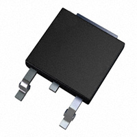
DPAK Power Surface Mount Package
The MBRD1035CTL employs the Schottky Barrier principle in a
large area metal−to−silicon power diode. State of the art geometry
features epitaxial construction with oxide passivation and metal
overlay contact. Ideally suited for low voltage, high frequency
switching power supplies, free wheeling diode and polarity protection
diodes.
http://onsemi.com
SCHOTTKY BARRIER
RECTIFIER
10 AMPERES
35 VOLTS
Features
• Highly Stable Oxide Passivated Junction
• Guardring for Stress Protection
• Matched Dual Die Construction −
•
•
•
•
•
•
May be Paralleled for High Current Output
High dv/dt Capability
Short Heat Sink Tap Manufactured − Not Sheared
Very Low Forward Voltage Drop
Epoxy Meets UL 94 V−0 @ 0.125 in
SBRD8 Prefix for Automotive and Other Applications Requiring
Unique Site and Control Change Requirements; AEC−Q101
Qualified and PPAP Capable
These Devices are Pb−Free and are RoHS Compliant*
DPAK
CASE 369C
1
4
3
MARKING DIAGRAM
YWW
B10
35CLG
Mechanical Characteristics:
• Case: Epoxy, Molded
• Weight: 0.4 Gram (Approximately)
• Finish: All External Surfaces Corrosion Resistant and Terminal
•
•
Leads are Readily Solderable
Lead and Mounting Surface Temperature for Soldering Purposes:
260°C Max. for 10 Seconds
ESD Rating:
♦ Human Body Model = 3B (> 8 kV)
♦ Machine Model = C (> 400 V)
Y
WW
B1035CL
G
= Year
= Work Week
= Device Code
= Pb−Free Package
ORDERING INFORMATION
See detailed ordering and shipping information in the package
dimensions section on page 3 of this data sheet.
*For additional information on our Pb−Free strategy and soldering details, please
download the ON Semiconductor Soldering and Mounting Techniques
Reference Manual, SOLDERRM/D.
© Semiconductor Components Industries, LLC, 2014
July, 2014 − Rev. 10
1
Publication Order Number:
MBRD1035CTL/D
�MBRD1035CTL Series, SBRD81035CTL Series
MAXIMUM RATINGS
Rating
Peak Repetitive Reverse Voltage
Working Peak Reverse Voltage
DC Blocking Voltage
Average Rectified Forward Current
(At Rated VR, TC = 115°C)
Per Leg
Per Package
Symbol
Value
Unit
VRRM
VRWM
VR
35
V
IO
A
5.0
10
Peak Repetitive Forward Current
(At Rated VR, Square Wave, 20 kHz, TC = 115°C)
Per Leg
IFRM
Non−Repetitive Peak Surge Current
(Surge applied at rated load conditions, halfwave, single phase, 60 Hz)
Per Package
IFSM
A
10
Storage / Operating Case Temperature
Operating Junction Temperature (Note 1)
Voltage Rate of Change (Rated VR, TJ = 25°C)
A
50
Tstg, Tc
−55 to +150
°C
TJ
−55 to +150
°C
dv/dt
10,000
V/ms
Stresses exceeding those listed in the Maximum Ratings table may damage the device. If any of these limits are exceeded, device functionality
should not be assumed, damage may occur and reliability may be affected.
1. The heat generated must be less than the thermal conductivity from Junction−to−Ambient: dPD/dTJ < 1/RqJA.
THERMAL CHARACTERISTICS
Rating
Symbol
Thermal Resistance, Junction−to−Case
Per Leg
RqJC
Thermal Resistance, Junction−to−Ambient (Note 2)
Per Leg
RqJA
Value
Unit
°C/W
3.0
°C/W
137
2. Rating applies when using minimum pad size, FR4 PC Board
ELECTRICAL CHARACTERISTICS
Rating
Symbol
Maximum Instantaneous Forward Voltage (Note 3) (See Figure 2)
Per Leg
(IF = 5 Amps, TJ = 25°C)
(IF = 5 Amps, TJ = 100°C)
(IF = 10 Amps, TJ = 25°C)
(IF = 10 Amps, TJ = 100°C)
VF
Maximum Instantaneous Reverse Current (Note 3) (See Figure 4)
Per Leg
(VR = 35 V, TJ = 25°C)
(VR = 35 V, TJ = 100°C)
(VR = 17.5 V, TJ = 25°C)
(VR = 17.5 V, TJ = 100°C)
IR
Value
Unit
V
0.47
0.41
0.56
0.55
mA
2.0
30
0.20
5.0
Product parametric performance is indicated in the Electrical Characteristics for the listed test conditions, unless otherwise noted. Product
performance may not be indicated by the Electrical Characteristics if operated under different conditions.
3. Pulse Test: Pulse Width ≤ 250 ms, Duty Cycle ≤ 2.0%
http://onsemi.com
2
�MBRD1035CTL Series, SBRD81035CTL Series
ORDERING INFORMATION
Device
Shipping†
Package
MBRD1035CTLG
75 Units / Rail
SBRD81035CTLG*
75 Units / Rail
DPAK
(Pb−Free)
MBRD1035CTLT4G
2,500 Units / Tape & Reel
SBRD81035CTLT4G*
2,500 Units / Tape & Reel
†For information on tape and reel specifications, including part orientation and tape sizes, please refer to our Tape and Reel Packaging
Specifications Brochure, BRD8011/D.
*SBRD8 Prefix for Automotive and Other Applications Requiring Unique Site and Control Change Requirements; AEC−Q101 Qualified and
PPAP Capable.
I F, INSTANTANEOUS FORWARD CURRENT (AMPS)
I F, INSTANTANEOUS FORWARD CURRENT (AMPS)
TYPICAL CHARACTERISTICS
100
TJ = 125°C
10
TJ = 100°C
TJ = 25°C
TJ = - 40°C
1.0
0.1
0.10
0.30
0.50
0.70
0.90
1.10
100
TJ = 125°C
10
TJ = 25°C
1.0
TJ = 100°C
0.1
0.10
VF, INSTANTANEOUS FORWARD VOLTAGE (VOLTS)
Figure 1. Typical Forward Voltage Per Leg
I R , MAXIMUM REVERSE CURRENT (AMPS)
I R , REVERSE CURRENT (AMPS)
0.50
0.70
0.90
1.10
Figure 2. Maximum Forward Voltage Per Leg
1E+0
100E-3
1E+0
100E-3
TJ = 125°C
10E-3
1E-3
TJ = 100°C
100E-6
TJ = 25°C
0
10
20
VR, REVERSE VOLTAGE (VOLTS)
TJ = 125°C
10E-3
TJ = 100°C
1E-3
100E-6
10E-6
1E-6
0.30
VF, MAXIMUM INSTANTANEOUS FORWARD VOLTAGE (VOLTS)
30
35
TJ = 25°C
10E-6
1E-6
0
10
20
VR, REVERSE VOLTAGE (VOLTS)
30
Figure 4. Maximum Reverse Current Per Leg
Figure 3. Typical Reverse Current Per Leg
http://onsemi.com
3
35
�PFO , AVERAGE POWER DISSIPATION (WATTS)
I O , AVERAGE FORWARD CURRENT (AMPS)
MBRD1035CTL Series, SBRD81035CTL Series
8.0
dc
7.0
SQUARE WAVE
(50% DUTY CYCLE)
6.0
5.0
Ipk/Io = p
4.0
Ipk/Io = 5
3.0
Ipk/Io = 10
2.0
Ipk/Io = 20
1.0
freq = 20 kHz
0
0
20
40
60
80
120
100
4.0
SQUARE WAVE
(50% DUTY CYCLE)
3.5
3.0
Ipk/Io = p
2.5
Ipk/Io = 5
2.0
Ipk/Io = 10
1.5
Ipk/Io = 20
1.0
0.5
0
0
140
1.0
1000
C, CAPACITANCE (pF)
TJ = 25°C
100
10
10
15
3.0
4.0
5.0
6.0
7.0
8.0
Figure 6. Forward Power Dissipation Per Leg
TJ , DERATED OPERATING TEMPERATURE ( ° C)
Figure 5. Current Derating Per Leg
5
2.0
IO, AVERAGE FORWARD CURRENT (AMPS)
TL, LEAD TEMPERATURE (°C)
0
dc
20
125
RqJA = 2.43°C/W
115
RqJA = 25°C/W
105
RqJA = 48°C/W
95
RqJA = 67.5°C/W
85
RqJA = 84°C/W
75
65
0
25
5
10
15
20
25
30
35
VR, DC REVERSE VOLTAGE (VOLTS)
VR, REVERSE VOLTAGE (VOLTS)
Figure 8. Typical Operating Temperature
Derating Per Leg *
Figure 7. Capacitance Per Leg
* Reverse power dissipation and the possibility of thermal runaway must be considered when operating this device under any reverse voltage conditions. Calculations of TJ therefore must include forward and reverse power effects. The allowable operating
TJ may be calculated from the equation:
TJ = TJmax − r(t)(Pf + Pr) where
r(t) = thermal impedance under given conditions,
Pf = forward power dissipation, and
Pr = reverse power dissipation
This graph displays the derated allowable TJ due to reverse bias under DC conditions only and is calculated as TJ = TJmax − r(t)Pr,
where r(t) = Rthja. For other power applications further calculations must be performed.
http://onsemi.com
4
�r (t) , TRANSIENT THERMAL RESISTANCE (NORMALIZED)
MBRD1035CTL Series, SBRD81035CTL Series
1.0
50%(DUTY CYCLE)
20%
10%
0.1 5.0%
2.0%
1.0%
SINGLE PULSE
0.01
0.00001
Rtjl(t) = Rtjl • r(t)
0.0001
0.001
0.01
0.1
10
1.0
100
1000
t, TIME (s)
r (t) , TRANSIENT THERMAL RESISTANCE (NORMALIZED)
Figure 9. Thermal Response Junction to Case (Per Leg)
1.0E+00
50% (DUTY CYCLE)
20%
1.0E-01
1.0E-02
10%
5.0%
2.0%
1.0%
1.0E-03
SINGLE PULSE
1.0E-04
0.00001
0.0001
Rtjl(t) = Rtjl • r(t)
0.001
0.01
0.1
1.0
10
t, TIME (s)
Figure 10. Thermal Response Junction to Ambient (Per Leg)
http://onsemi.com
5
100
1000
10000
�MBRD1035CTL Series, SBRD81035CTL Series
PACKAGE DIMENSIONS
DPAK (SINGLE GAUGE)
CASE 369C
ISSUE D
NOTES:
1. DIMENSIONING AND TOLERANCING PER ASME
Y14.5M, 1994.
2. CONTROLLING DIMENSION: INCHES.
3. THERMAL PAD CONTOUR OPTIONAL WITHIN DIMENSIONS b3, L3 and Z.
4. DIMENSIONS D AND E DO NOT INCLUDE MOLD
FLASH, PROTRUSIONS, OR BURRS. MOLD
FLASH, PROTRUSIONS, OR GATE BURRS SHALL
NOT EXCEED 0.006 INCHES PER SIDE.
5. DIMENSIONS D AND E ARE DETERMINED AT THE
OUTERMOST EXTREMES OF THE PLASTIC BODY.
6. DATUMS A AND B ARE DETERMINED AT DATUM
PLANE H.
C
A
A
E
b3
c2
B
4
L3
Z
D
1
2
H
DETAIL A
3
L4
b2
e
c
b
0.005 (0.13)
M
C
H
L2
GAUGE
PLANE
C
L
SEATING
PLANE
A1
L1
DETAIL A
ROTATED 905 CW
DIM
A
A1
b
b2
b3
c
c2
D
E
e
H
L
L1
L2
L3
L4
Z
INCHES
MIN
MAX
0.086 0.094
0.000 0.005
0.025 0.035
0.030 0.045
0.180 0.215
0.018 0.024
0.018 0.024
0.235 0.245
0.250 0.265
0.090 BSC
0.370 0.410
0.055 0.070
0.108 REF
0.020 BSC
0.035 0.050
−−− 0.040
0.155
−−−
MILLIMETERS
MIN
MAX
2.18
2.38
0.00
0.13
0.63
0.89
0.76
1.14
4.57
5.46
0.46
0.61
0.46
0.61
5.97
6.22
6.35
6.73
2.29 BSC
9.40 10.41
1.40
1.78
2.74 REF
0.51 BSC
0.89
1.27
−−−
1.01
3.93
−−−
SOLDERING FOOTPRINT*
6.20
0.244
2.58
0.102
5.80
0.228
3.00
0.118
1.60
0.063
6.17
0.243
SCALE 3:1
mm Ǔ
ǒinches
*For additional information on our Pb−Free strategy and soldering
details, please download the ON Semiconductor Soldering and
Mounting Techniques Reference Manual, SOLDERRM/D.
ON Semiconductor and
are registered trademarks of Semiconductor Components Industries, LLC (SCILLC). SCILLC reserves the right to make changes without further notice
to any products herein. SCILLC makes no warranty, representation or guarantee regarding the suitability of its products for any particular purpose, nor does SCILLC assume any liability
arising out of the application or use of any product or circuit, and specifically disclaims any and all liability, including without limitation special, consequential or incidental damages.
“Typical” parameters which may be provided in SCILLC data sheets and/or specifications can and do vary in different applications and actual performance may vary over time. All
operating parameters, including “Typicals” must be validated for each customer application by customer’s technical experts. SCILLC does not convey any license under its patent rights
nor the rights of others. SCILLC products are not designed, intended, or authorized for use as components in systems intended for surgical implant into the body, or other applications
intended to support or sustain life, or for any other application in which the failure of the SCILLC product could create a situation where personal injury or death may occur. Should
Buyer purchase or use SCILLC products for any such unintended or unauthorized application, Buyer shall indemnify and hold SCILLC and its officers, employees, subsidiaries, affiliates,
and distributors harmless against all claims, costs, damages, and expenses, and reasonable attorney fees arising out of, directly or indirectly, any claim of personal injury or death
associated with such unintended or unauthorized use, even if such claim alleges that SCILLC was negligent regarding the design or manufacture of the part. SCILLC is an Equal
Opportunity/Affirmative Action Employer. This literature is subject to all applicable copyright laws and is not for resale in any manner.
PUBLICATION ORDERING INFORMATION
LITERATURE FULFILLMENT:
Literature Distribution Center for ON Semiconductor
P.O. Box 5163, Denver, Colorado 80217 USA
Phone: 303−675−2175 or 800−344−3860 Toll Free USA/Canada
Fax: 303−675−2176 or 800−344−3867 Toll Free USA/Canada
Email: orderlit@onsemi.com
N. American Technical Support: 800−282−9855 Toll Free
USA/Canada
Europe, Middle East and Africa Technical Support:
Phone: 421 33 790 2910
Japan Customer Focus Center
Phone: 81−3−5817−1050
http://onsemi.com
6
ON Semiconductor Website: www.onsemi.com
Order Literature: http://www.onsemi.com/orderlit
For additional information, please contact your local
Sales Representative
MBRD1035CTL/D
�


 工商网监
湘ICP备2023018690号
工商网监
湘ICP备2023018690号
