OKDL-T/12-W12-xxx-C
www.murata-ps.com
12A Digital PoL DC-DC Converter Series
Typical unit
FEATURES
PRODUCT OVERVIEW
Small package: 12.2 x 12.2 x 8.0 mm (0.48 x 0.48 x 0.315 in)
The OKDL-T/12-W12 is a high efficiency,
digital point-of-Load (PoL) DC-DC power
converter capable of delivering 12A/60W.
Designed for a minimal footprint, the high
power-density LGA module measures
just 12.2 x 12.2 x 8.0 mm (0.48 x 0.48 x
0.315 in).
0.6 V - 5 V output voltage range
High efficiency, typ. 95.4% at 12Vin, 5Vout and 50% load
Configuration Control and Monitoring via PMBus™
Adaptive compensation of PWM control loop & fast loop
transient response
Synchonization input & phase spreading/interleaving
Voltage Tracking & Voltage margining
MTBF 24 Mh
PMBus™ compatibility allows monitoring and confi guration of critical systemlevel performance requirements.
Apart from standard PoL performance
and safety features like OVP, OCP, OTP,
and UVLO, these digital converters have
advanced features: Adaptive compensation of PWM control loop, fast loop
transient response, synchronization,
and phase spreading. These converters
are ideal for use in telecommunications, networking, and distributed power
applications.
For narrow board pitch applications (15 mm/0.6 in)
Pre-bias start-up & shut down
Monotonic & Soft start Power up
Input under voltage shutdown; OTP, output OVP, OCP
Remote control & Power Good
Applications
Distributed power architectures
Intermediate bus voltage applications
Differential sense pins
Servers and storage applications
Voltage setting via pin-strap or PMBus™
Advanced Configurable via Graphical User Interface
Network equipment
ISO 9001/14001 certified supplier
Highly automated manufacturing ensures quality
PART NUMBER STRUCTURE
OKD L - T / 12 - W12 - xxx - C
Digital Non-isolated PoL
LGA Package
Trimmable Output
Voltage Range
0.6 - 5Vdc
Maximum Rated Output
Current in Amps
RoHS Hazardous
Substance Compliance
C = RoHS-6 (does not claim EU RoHS exemption
7b – lead in solder)
Software Configuration Digits
(001 is positive turn-on logic)
(002 is negative turn-on logic)*
Input Voltage Range
4.5-14Vdc
*Special quantity order is required;
contact Murata Power Solutions for
MOQ and lead times.
PM
www.murata-ps.com/support
MDC_OKDL-T/12-W12-xxx-C.A03 Page 1 of 31
�OKDL-T/12-W12-xxx-C
12A Digital PoL DC-DC Converter Series
ORDERING GUIDE
Model Number
OKDL-T/12-W12-001-C
Output
0.6-5.0 V, 12 A/ 60 W
Absolute Maximum Ratings
Characteristics
TP1
Operating temperature (see Thermal Consideration section)
TS
Storage temperature
VI
Input voltage (See Operating Information Section for input and output voltage relations)
Logic I/O voltage
CTRL, SA0, SA1, SALERT, SCL, SDA, VSET, SYNC, PG, CS_VTRK
Ground voltage differential -S, PREF, GND
Analog pin voltage
VO, +S
General and Safety
Safety
Calculated MTBF
Min
-40
-40
-0.3
-0.3
-0.3
-0.3
Conditions
Designed for UL/IEC/EN 60950 1
Telcordia SR-332, Issue 2 Method 1
Stress in excess of Absolute Maximum Ratings may cause permanent
damage. Absolute Maximum Ratings, sometimes referred to as no
destruction limits, are normally tested with one parameter at a time
exceeding the limits in the Electrical Specification. If exposed to stress
above these limits, function and performance may degrade in an
unspecified manner.
Configuration File
This product is designed with a digital control circuit. The control
circuit uses a configuration file which determines the functionality
and performance of the product. The Electrical Specification table
shows parameter values of functionality and performance with the
Min
Typ
Typ
24
Max
120
125
18
4
0.3
5.5
Max
Unit
°C
°C
V
V
V
V
Unit
Mhrs
default configuration file, unless otherwise specified. The default
configuration file is designed to fit most application needs with focus
on high efficiency. If different characteristics are required it is possible to change the configuration file to optimize certain performance
characteristics.
In this Technical specification examples are included to show the
possibilities with digital control. See Operating Information section for
information about trade offs when optimizing certain key performance
characteristics.
VIN
VOUT
CI
CO
GND
+Sense
-Sense
CTRL
PGOOD
SDA
SCL
Controller and digital interface
SA0
SALERT
SYNC
CS_VTRK
VSET
SA1
PREF
Fundamental Circuit Diagram
www.murata-ps.com/support
MDC_OKDL-T/12-W12-xxx-C.A03 Page 2 of 31
�OKDL-T/12-W12-xxx-C
12A Digital PoL DC-DC Converter Series
Electrical Specifications
TP1 = -30 to +95°C, VI = 4.5 to 14 V, VI > VO + 1.0 V
Typical values given at: TP1 = +25°C, VI = 12.0 V, max IO, unless otherwise specified under Conditions.
Default configuration file, 190 10-CDA 102 0370/001. VO defined by pin strap.
External CIN = 47 μF ceramic + 270 μF/10 mΩ electrolytic, COUT = 3x100 μF + 0.1 μF ceramic.
See Operating Information section for selection of capacitor types. Sense pins are connected to the output pins.
Characteristics
VI
Input voltage
Output voltage without pin strap
Output voltage adjustment range
Output voltage adjustment including PMBus margining
Output voltage set-point resolution
Output voltage accuracy
Internal resistance +S/-S to VOUT/GND
+S bias current
-S bias current
VO
Line regulation
IO = max IO
Load regulation
IO = 0 - 100%
VOac
Output ripple & noise
(up to 20 MHz)
IO
Output current
Static input current at max IO
Ilim
Current limit threshold
Isc
Short circuit current
Efficiency
IO = max IO
Power dissipation at max IO
Pli
Input idling power
PCTRL
Input standby power
Typ
IO = 0
Max
14
0
0.60
0.50
5.0
5.25
1.2
Including line, load, temp
-1
1
47
50
-35
1
2
3
4
7
1
1
1
2
2
10
10
11
19
25
VO = 0.6 V
VO = 1.2 V
VO = 1.8 V
VO = 3.3 V
VO = 5.0 V
VO = 0.6 V
VO = 1.2 V
VO = 1.8 V
VO = 3.3 V
VO = 5.0 V
VO = 0.6 V
VO = 1.2 V
VO = 1.8 V
VO = 3.3 V
VO = 5.0 V
VO = 0.6 V
VO = 1.2 V
VO = 1.8 V
VO = 3.3 V
VO = 5.0 V
RMS, hiccup mode,
VO = 3.3 V, 4 mΩ short
50% of max IO
Pd
Min
4.5
0
IS
Conditions
mV
mV
mVp-p
12
0.7
1.3
2.0
3.5
5.2
15
3
Unit
V
V
V
V
mV
% VO
Ω
μA
μA
A
A
17
A
A
VO = 0.6 V
VO = 1.2 V
VO = 1.8 V
VO = 3.3 V
VO = 5.0 V
VO = 0.6 V
VO = 1.2 V
VO = 1.8 V
VO = 3.3 V
VO = 5.0 V
VO = 0.6 V
VO = 1.2 V
VO = 1.8 V
VO = 3.3 V
VO = 5.0 V
78.8
87.5
90.8
94.1
95.4
81.3
89.0
91.8
94.6
95.8
1.66
1.78
1.93
2.24
2.63
VO = 0.6 V
VO = 1.2 V
VO = 1.8 V
VO = 3.3 V
VO = 5.0 V
0.70
0.70
0.71
0.80
0.92
W
Turned off with CTRL-pin
0.25
W
%
%
W
www.murata-ps.com/support
MDC_OKDL-T/12-W12-xxx-C.A03 Page 3 of 31
�OKDL-T/12-W12-xxx-C
12A Digital PoL DC-DC Converter Series
Characteristics
CI
Internal input capacitance
CO
Internal output capacitance
COUT
Total output capacitance
Vtr1
Load transient peak voltage deviation
ttr1
Load transient recovery time
Conditions
VI = 0 V
VO = 0 V
VO = 3.3 V
VO = 5.0 V
Effective capacitance
Note 1
Min
Switching frequency range
Switching frequency set-point accuracy
External Sync Duty Cycle
Input Clock Frequency Drift Tolerance
Input Under Voltage Lockout
(hardware controlled)
Input Over Voltage Lockout
(hardware controlled)
Threshold, VUVLO
Load step 25-75-25% of max IO, di/dt
= 1.5 A/μs
CO=3x100 μF + 270 μF
VO = 3.3 V
PMBus configurable
FREQUENCY_SWITCH
Note 2
External clock source
-10
40
-10
Rising edge
3.8
Hysteresis
Threshold, VOVLO
Input rising
Threshold range
Threshold range
Input Under/Over Voltage
Protection,
IUVP/ IOVP
UVP threshold range
Fault response
OCP threshold
Over Current Protection,
OCP
Over Temperature Protection,
OTP
Over Temperature Shutdown
(hardware controlled)
OCP threshold range
300-1000
kHz
±5
4.1
10
60
10
%
%
%
4.4
V
15.2
V
16
V
V
V
V
PMBus configurable
VIN_UV_FAULT_LIMIT
0-14.7
V
14.4
V
PMBus configurable
VIN_OV_FAULT_LIMIT
0-14.7
V
VIN_UV_FAULT_RESPONSE
VIN_OV_FAULT_RESPONSE
PMBus configurable
VOUT_UV_FAULT_LIMIT
PMBus configurable
VOUT_OV_FAULT_LIMIT
VOUT_UV_FAULT_RESPONSE
VOUT_OV_FAULT_RESPONSE
Set value
PMBus configurable
IOUT_OC_FAULT_LIMIT
IOUT_OC_FAULT_RESPONSE
OTP threshold
Note 4
PMBus configurable
OT_FAULT_LIMIT
PMBus configurable
OTP hysteresis
kHz
4.1
Fault response
OTP threshold range
600
0-14.7
PMBus configurable
VIN_OFF
OVP threshold
OVP threshold range
μs
V
UVP threshold
Output voltage
Over/Under Voltage Protection,
OVP/UVP
25
V
Set point accuracy
Fault response
mV
3.8
IOVP threshold
IOVP threshold range
60
0-14.7
IUVP threshold
IUVP threshold range
μF
4.35
PMBus configurable
VIN_ON
Threshold
Input Turn-Off Voltage
14.3
Unit
μF
μF
0.24
Threshold
Input Turn-On Voltage
Max
55
Switching frequency
Fsw
Typ
47
47
24
15
Fault response
OT_FAULT_RESPONSE
Threshold
Hysteresis
Accuracy
Note 4
-150
150
Shutdown, make continuous restarts at 700 ms
interval (hiccup). Note 3
85
mV
% VO
0-100
% VO
115
% VO
100-115
% VO
Shutdown, make continuous restarts at 700 ms
interval (hiccup). Note 3
16
0-18
Shutdown, make continuous restarts at 700 ms
interval (hiccup). Note 3.
120
-40…+120
15
Shutdown, make continuous restarts at 700 ms
interval (hiccup). Note 3
150
20
±20
A
A
°C
°C
°C
°C
°C
°C
www.murata-ps.com/support
MDC_OKDL-T/12-W12-xxx-C.A03 Page 4 of 31
�OKDL-T/12-W12-xxx-C
12A Digital PoL DC-DC Converter Series
Characteristics
VOL
Logic output low signal level
VOH
Logic output high signal level
IOL
IOH
VIL
VIH
IIL_CTRL
II_LEAK
fSMB
Logic output low sink current
Logic output high source current
Logic input low threshold
Logic input high threshold
Logic input low sink current
Logic leakage current
SMBus Operating frequency
TBUF
SMBus Bus free time
tset
thold
SMBus SDA setup time from SCL
SMBus SDA hold time from SCL
SMBus START/STOP condition setup/hold time from SCL
SCL low period
SCL high period
Tlow
Thigh
Initialization time
Conditions
Min
SCL, SDA, SYNC, SALERT, PG
Sink/source current = 4 mA
2.8
SCL, SDA, CTRL, SYNC
4
4
0.8
2
CTRL
SCL, SDA, SYNC, SALERT, PG
0.5
10
400
STOP bit to START bit
See section SMBus – Timing
Note 5
Delay accuracy
100
300
600
1.3
0.6
ns
ns
ns
μs
μs
PMBus configurable
TON_DELAY
TON_DELAY value sent versus readback
Actual delay duration versus TON_DELAY read-back
Note 5
Ramp duration range
Ramp set resolution
Ramp set accuracy
Ramp time accuracy
PMBus configurable
TON_RISE
Varies with VO
TON_RISE value sent versus read-back
Actual ramp duration versus TON_RISE
read-back
Signal level
PG threshold
PG thresholds range
(Non-tracking only)
Power Good , PG
1-145
ms
0.6
ms
±0.5 x Delay set resolution
ms
ms
ms
1 - (255 x Ramp set resolution)
ms
0.4
1
±0.5 x Ramp set resolution
VO = 0.6 V
VO = 1.2 – 3.3 V
VO = 5.0 V
Rising
Falling
Tracking mode
See section Voltage Tracking
PMBus configurable
POWER_GOOD_ON
POWER_GOOD_OFF
ms
ms
10
Signal duration
Compensation Calibration
23
10
±0.8
Ramp duration
Soft-start
Rise Time
(0-100% of VO)
mA
mA
V
V
mA
uA
kHz
μs
Delay set resolution
Delay set accuracy
Unit
V
1.3
From VI > VUVLO to ready to be enabled
Delay duration range
Max
0.4
V
Delay duration
Soft-start
On Delay Time
Typ
ms
ms
±10
μs
5
3.5
2.5
2
ms
% VO
90
85
% VO
% VO
450
mV
0
100
% VO
PG delay
From VO reaching target to PG assertion
11
ms
Enabled compensation calibration
(default)
Tracking mode
See section Voltage Tracking
20
ms
PG delay
From VO reaching PG rising threshold to
PG assertion
0
ms
Tracking mode
See section Voltage Tracking
20
ms
Disabled compensation calibration
Tracking Input Voltage Range
Tracking Accuracy
CS_VTRK pin
Note 6
0
1.2
V
-100
100
mV
www.murata-ps.com/support
MDC_OKDL-T/12-W12-xxx-C.A03 Page 5 of 31
�OKDL-T/12-W12-xxx-C
12A Digital PoL DC-DC Converter Series
Characteristics
Conditions
Min
Input voltage
READ_VIN
Output voltage
READ_VOUT
Monitoring accuracy
Output current
READ_IOUT
Note 7
TP1 = 0-95°C, VI = 4.5-14 V,
IO > 5 A
TP1 = 0-95°C, VI = 4.5-14 V,
IO < 5 A
Temperature
READ_
TEMPERATURE_1
Note 4
-5
Duty cycle < 10%
-3
Duty cycle > 10%
-1
Duty cycle
READ_DUTY_CYCLE
Note 1. Value refers to total (internal + external) effective output capacitance. Capacitance derating with VO typical for
ceramic capacitors (bias characteristics) and temperature variations must be considered for the external capacitor(s).
See section External Output Capacitors.
Note 2. A switching frequency close to 475 kHz should not be used since this frequency represents a boundary of
two operational modes of the product. There are configuration changes to consider when changing the switching
frequency, see section Switching Frequency.
Note 3.The restart interval is configurable between 100ms and 700ms in 100ms steps. Severe overcurrent faults
occurring with VO > 2.5V may result in a restart interval of 1200 ms instead of the configured value. See operating
conditions for other fault response alternatives.
Typ
Max
Unit
±3
% VI
±1
% VO
±8.5
% IO
±0.4
A
±0.5
5
°C
3
%
1
%
Note 4. Temperature measured internally at temperature position P3. See section Over Temperature Protection.
Note 5. Same specification applies for soft-stop and TOFF_DELAY/TOFF_FALL if enabled. The internal ramp and delay
generators can only achieve certain discrete timing values. A written TON/OFF_DELAY or TON/OFF_RISE value will
be rounded to the closest achievable value, thus a command read-back provides the actual set value. See section
Soft-Start and Soft-Stop.
Note 6.Larger tracking input range is provided by external resistor divider, see section Voltage Tracking.
Note 7. At VO > 3.5V and VO / VI in the approximate range 55-70% there may be an additional current monitoring
inaccuracy on the negative side up to -1 A.
www.murata-ps.com/support
MDC_OKDL-T/12-W12-xxx-C.A03 Page 6 of 31
�OKDL-T/12-W12-xxx-C
12A Digital PoL DC-DC Converter Series
Typical Characteristics, VO = 0.6 V
Default Configuration, TP1 = +25°C
Power Dissipation
Efficiency
[%]
[W]
90
2.5
85
80
VI
75
4.5 V
70
2.0
VI
4.5 V
1.5
5V
5V
1.0
65
12 V
12 V
60
14 V
14 V
0.5
55
50
0
2
4
6
8
10
12
0.0
0
[A]
2
4
6
8
10
Efficiency vs. load current and input voltage.
Dissipated power vs. load current and input voltage.
Output Current Derating
Current Limit Characteristics
[A]
12
[A]
[V]
12
0.75
10
3.0 m/s
8
2.0 m/s
6
1.0 m/s
0.5 m/s
4
Nat. Conv.
2
0.60
VI
0.45
4.5 V
5V
0.30
12 V
14 V
0.15
0.00
0
85
90
95
100
105
[°C]
12
13
14
15
16
17 [A]
Available load current vs. ambient air temperature and airflow at
VI = 12 V. See section Thermal Consideration.
Output voltage vs. load current and input voltage.
Output Ripple and Noise
Transient Response
Fundamental output voltage ripple at VI = 12 V, CO = 3x100 μF, IO = 12 A.
Scale: 5 mV/div, 1 μs/div, 20 MHz bandwidth.
See section Output Ripple and Noise.
Output voltage response to load current step change (3–9–3 A) at
VI = 12 V, CO = 3x100 μF + 270 μF/10m. Default compensation settings.
Scale: 50 mV/div, 5 A/div, 50 μs/div.
www.murata-ps.com/support
MDC_OKDL-T/12-W12-xxx-C.A03 Page 7 of 31
�OKDL-T/12-W12-xxx-C
12A Digital PoL DC-DC Converter Series
Typical Characteristics, VO = 1.2 V
Default Configuration, TP1 = +25°C
Efficiency
Power Dissipation
[%]
[W]
95
2.5
90
2.0
85
VI
VI
80
4.5 V
1.5
4.5 V
75
5V
5V
1.0
70
12 V
12 V
65
14 V
14 V
0.5
60
55
0.0
0
2
4
6
8
10
12
0
[A]
2
4
6
8
10
Efficiency vs. load current and input voltage.
Dissipated power vs. load current and input voltage.
Output Current Derating
Current Limit Characteristics
[A]
12
[A]
[V]
12
1.50
10
3.0 m/s
8
2.0 m/s
6
1.0 m/s
VI
1.20
4.5 V
0.90
0.5 m/s
4
5V
0.60
12 V
Nat. Conv.
14 V
0.30
2
0
85
90
95
100
105
0.00
[°C]
12
13
14
15
16
17
[A]
Available load current vs. ambient air temperature and airflow at
VI = 12 V. See section Thermal Consideration.
Output voltage vs. load current and input voltage.
Output Ripple and Noise
Transient Response
Fundamental output voltage ripple at VI = 12 V, CO = 3x100 μF, IO = 12 A.
Scale: 5 mV/div, 1 μs/div, 20 MHz bandwidth.
See section Output Ripple and Noise.
Output voltage response to load current step change (3–9–3 A) at
VI = 12 V, CO = 3x100 μF + 270 μF/10m. Default compensation settings.
Scale: 50 mV/div, 5 A/div, 50 μs/div.
www.murata-ps.com/support
MDC_OKDL-T/12-W12-xxx-C.A03 Page 8 of 31
�OKDL-T/12-W12-xxx-C
12A Digital PoL DC-DC Converter Series
Typical Characteristics, VO = 1.8 V
Default Configuration, TP1 = +25°C
Efficiency
Power Dissipation
[%]
[W]
100
2.5
95
2.0
90
VI
VI
85
4.5 V
1.5
4.5 V
80
5V
5V
75
1.0
12 V
70
14 V
12 V
14 V
0.5
65
60
0
2
4
6
8
10
12
0.0
0
[A]
2
4
6
8
10
Efficiency vs. load current and input voltage.
Dissipated power vs. load current and input voltage.
Output Current Derating
Current Limit Characteristics
[A]
12
[A]
[V]
12
2.0
10
3.0 m/s
8
2.0 m/s
6
1.0 m/s
0.5 m/s
4
Nat. Conv.
VI
1.6
4.5 V
1.2
5V
0.8
12 V
14 V
0.4
2
0.0
0
85
90
95
100
105
12
13
14
15
16
[°C]
17
[A]
Available load current vs. ambient air temperature and airflow at
VI = 12 V. See section Thermal Consideration.
Output voltage vs. load current and input voltage.
Output Ripple and Noise
Transient Response
Fundamental output voltage ripple at VI = 12 V, CO = 3x100 μF, IO = 12 A.
Scale: 5 mV/div, 1 μs/div, 20 MHz bandwidth.
See section Output Ripple and Noise.
Output voltage response to load current step change (3–9–3 A) at
VI = 12 V, CO = 3x100 μF + 270 μF/10m. Default compensation settings.
Scale: 50 mV/div, 5 A/div, 50 μs/div.
www.murata-ps.com/support
MDC_OKDL-T/12-W12-xxx-C.A03 Page 9 of 31
�OKDL-T/12-W12-xxx-C
12A Digital PoL DC-DC Converter Series
Typical Characteristics, VO = 3.3 V
Default Configuration, TP1 = +25°C
Efficiency
Power Dissipation
[%]
[W]
100
2.5
95
2.0
VI
VI
90
4.5 V
85
1.5
4.5 V
5V
5V
1.0
12 V
12 V
80
14 V
75
70
14 V
0.5
0.0
0
2
4
6
8
10
12
0
[A]
2
4
6
8
10
Efficiency vs. load current and input voltage.
Dissipated power vs. load current and input voltage.
Output Current Derating
Current Limit Characteristics
[A]
12
[A]
[V]
12
3.6
10
3.0 m/s
3.0
8
2.0 m/s
2.4
6
1.0 m/s
1.8
0.5 m/s
4
VI
4.5 V
5V
12 V
1.2
Nat. Conv.
14 V
0.6
2
0.0
0
85
90
95
100
105
[°C]
12
13
14
15
16
17
[A]
Available load current vs. ambient air temperature and airflow at
VI = 12 V. See section Thermal Consideration.
Output voltage vs. load current and input voltage.
Output Ripple and Noise
Transient Response
Fundamental output voltage ripple at VI = 12 V, CO = 3x100 μF, IO = 12 A.
Scale: 5 mV/div, 1 μs/div, 20 MHz bandwidth.
See section Output Ripple and Noise.
Output voltage response to load current step change (3–9–3 A) at
VI = 12 V, CO = 3x100 μF + 270 μF/10m. Default compensation settings.
Scale: 50 mV/div, 5 A/div, 50 μs/div.
www.murata-ps.com/support
MDC_OKDL-T/12-W12-xxx-C.A03 Page 10 of 31
�OKDL-T/12-W12-xxx-C
12A Digital PoL DC-DC Converter Series
Typical Characteristics, VO = 5.0 V
Default Configuration, TP1 = +25°C
Efficiency
Power Dissipation
[W]
[%]
100
3.5
3.0
95
VI
90
6V
85
9.6 V
80
12 V
14 V
75
VI
2.5
6V
2.0
9.6 V
1.5
12 V
1.0
14 V
0.5
70
0
2
4
6
8
10
0.0
12 [A]
0
2
4
6
8
10
Efficiency vs. load current and input voltage.
Dissipated power vs. load current and input voltage.
Output Current Derating
Current Limit Characteristics
[A]
12
[A]
[V]
12
6.0
10
3.0 m/s
8
2.0 m/s
6
1.0 m/s
5.0
VI
4.0
6V
3.0
9.6 V
0.5 m/s
4
12 V
2.0
Nat. Conv.
2
14 V
1.0
0
80
85
90
95
100
0.0
[°C]
12
13
14
15
16
17
[A]
Available load current vs. ambient air temperature and airflow at
VI = 12 V. See section Thermal Consideration.
Output voltage vs. load current and input voltage.
Output Ripple and Noise
Transient Response
Fundamental output voltage ripple at VI = 12 V, CO = 3x100 μF, IO = 12 A.
Scale: 5 mV/div, 1 μs/div, 20 MHz bandwidth.
See section Output Ripple and Noise.
Output voltage response to load current step change (3–9–3 A) at
VI = 12 V, CO = 3x100 μF + 270 μF/10m. Default compensation settings.
Scale: 50 mV/div, 5 A/div, 50 μs/div.
www.murata-ps.com/support
MDC_OKDL-T/12-W12-xxx-C.A03 Page 11 of 31
�OKDL-T/12-W12-xxx-C
12A Digital PoL DC-DC Converter Series
Typical Characteristics
Default Configuration, TP1 = +25°C, VO = 3.3 V
Start-up by input source
Shut-down by input source
VI
VI
VO
VO
PG
PG
Start-up enabled by applying VI. TON_DELAY = TON_RISE = 10 ms (default).
VI = 12 V, IO = max IO, PG pulled up to VO.
Scale: 10 or 2 V/div, 10 ms/div.
Shut-down by removing VI.
VI = 12 V, IO = max IO, PG pulled up to VO.
Scale: 10 or 2 V/div, 1 ms/div.
Start-up by CTRL signal
Shutdown by CTRL signal
CTRL
CTRL
VO
VO
PG
PG
Start-up enabled by CTRL signal. TON_DELAY = TON_RISE = 10 ms (default).
VI = 12 V, IO = max IO, PG pulled up to VO.
Scale: 2 V/div, 10 ms/div.
Shut-down by CTRL signal.
VI = 12 V, IO = max IO, PG pulled up to VO.
Scale: 2 V/div, 1 ms/div.
www.murata-ps.com/support
MDC_OKDL-T/12-W12-xxx-C.A03 Page 12 of 31
�OKDL-T/12-W12-xxx-C
12A Digital PoL DC-DC Converter Series
Conducted EMI Input terminal value (typical for default configuration)
Output Ripple and Noise
Output ripple and noise is measured according to figure below.
A 50 mm conductor works as a small inductor forming together
with the two capacitances a damped filter.
50 mm conductor
Vout
S
co
Tantalum
Capacitor
10 μF
Ceramic
Capacitor
0.1 μF
Load
EMC Specification
Conducted EMI is measured according to the test set-up below. The
fundamental switching frequency is 600 kHz.
S
GND
50 mm conductor
BNC-contact to
oscilloscope
Output ripple and noise test set-up
EMI without filter
To spectrum
analyzer
RF Current probe
1kHz – 50MHz
Battery
supply
The digital compensation of the product is designed to automatically
provide stability, accurate line and load regulation and good transient
performance for a wide range of operating conditions (switching
frequency, input voltage, output voltage, output capacitance). Inherent
from the implementation and normal to the product there will be some
low-frequency noise or wander at the output, in addition to the fundamental switching frequency output ripple. The total output ripple and noise is
maintained at a low level.
Resistive
load
DUT
C1
50mm
C1 = 10uF / 600VDC
Feed- Thru RF capacitor
800mm
200mm
VI=12 V, VO=3.3 V, IO=12 A, CO=3x100 μF,10 mV/div, 50 μs/div
Test set-up conducted emission, power lead
Example of low frequency noise at the output
Layout Recommendations
The radiated EMI performance of the product will depend on the PWB
layout and ground layer design. It is also important to consider the standoff of the product. If a ground layer is used, it should be connected to the
output of the product and the equipment ground or chassis.
A ground layer will increase the stray capacitance in the PWB and
improve the high frequency EMC performance.
www.murata-ps.com/support
MDC_OKDL-T/12-W12-xxx-C.A03 Page 13 of 31
�OKDL-T/12-W12-xxx-C
12A Digital PoL DC-DC Converter Series
Operating information
Power Management Overview
This product is equipped with a PMBus™ interface. The product
incorporates a wide range of readable and configurable power management features that are simple to implement
with a minimum of external components. Additionally, the product
includes protection features that continuously safeguard the load from
damage due to unexpected system faults. A fault is also shown as an
alert on the SALERT pin.
The product is delivered with a default configuration suitable for a
wide range of operation in terms of input voltage, output voltage, and
load. The configuration is stored in an internal Non-Volatile Memory
(NVM). All power management functions can be reconfigured using
the PMBus™ interface. Please contact your local Murata Power
Solutions representative for design support of custom configurations or appropriate SW tools for design and download of your own
configurations.
Input Under Voltage Lockout, UVLO
The product provides a non-configurable under voltage lockout (UVLO)
circuit that monitors the internal supply of the converter. Below a certain input voltage level the internal supply will be too low for proper
operation and the product will be in under voltage lockout, not switching or responding to the CTRL pin or to PMBus™ commands.
Input Over Voltage Lockout, OVLO
The product provides a non-configurable over voltage lockout (OVLO)
circuit that will shut down the product when the input voltage rises
above a certain level. The product will not switch, respond to the CTRL
pin or to PMBus™ commands when being in over voltage lockout.
Input Turn-On and Turn-Off Voltage
The product monitors the input voltage and will turn-on and turn-off
the output at configured levels (assuming the product is enabled by
CTRL pin or PMBus™). The default turn-on input voltage level is 4.35
V whereas the corresponding turn-off input voltage level is 3.8 V. The
turn-on and turn-off levels may be reconfigured using the PMBus™
commands VIN_ON and VIN_OFF.
Input Under Voltage Protection (IUVP)
The product monitors the input voltage continously and will respond
as configured when the input voltage falls below the configured
threshold level. The product can respond in a number of ways as
follows:
1. Continue operating without interruption.
2. Continue operating for a given delay period, followed by an output
voltage shutdown if the fault still exists.
3. Immediate and definite shutdown of output voltage until the fault is
cleared by PMBus™ or the output voltage is re-enabled.
4. Immediate shutdown of output voltage while the fault is present.
Operation resumes and the output is enabled when the fault condition no longer exists.
The default response is 4. The IUVP function can be reconfigured using the PMBus™ commands VIN_UV_FAULT_LIMIT and
VIN_UV_FAULT_RESPONSE.
Input Over Voltage Protection (IOVP)
The product monitors the input voltage continously and will respond
as configured when the input voltage rises above the configured
threshold level. Refer to section “Input Under Voltage Protection” for
response configuration options and default setting.
Input and Output Impedance
The impedance of both the input source and the load will interact with
the impedance of the product. It is important that the input source
has low characteristic impedance. If the input voltage source contains
significant inductance, the addition of a capacitor with low ESR at the
input of the product will ensure stable operation.
External Input Capacitors
The input ripple RMS current in a buck converter can be estimated to
Eq. 1. IinputRMS I load D �1 � D � ,
where I load is the output load current and Dis the duty cycle. The maxi
mum load ripple current becomes I load 2. The ripple current is
divided into three parts, i.e., currents in the input source, external
input capacitor, and internal input capacitor. How the current is
divided depends on the impedance of the input source, ESR and
capacitance values in the capacitors.
For most applications non-tantalum capacitors are preferred due
to the robustness of such capacitors to accommodate high inrush
currents of systems being powered from very low impedance sources.
It is recommended to use a combination of ceramic capacitors and
low-ESR electrolytic/polymer bulk capacitors. The low ESR of ceramic
capacitors effectively limits the input ripple voltage level, while the
bulk capacitance minimizes deviations in the input voltage at large
load transients.
It is recommended to use at least 47 uF of ceramic input capacitance. At duty cycles between 25% and 75% where the input ripple
current increases (see Eq. 1), additional ceramic capacitance will help
to keep the input ripple voltage low. The required bulk capacitance
depends on the impedance of the input source and the load transient levels at the output. In general a low-ESR bulk capacitor of at
least 100 uF is recommended. The larger the duty cycle is, the larger
impact an output load step will have on the input side, thus the larger
bulk capacitance is required to limit the input voltage deviation.
If several products are connected in a phase spreading setup the
amount of input capacitance per product can be reduced.
Input Capacitors must be placed closely and with low impedance
connections to the VIN and GND pins in order to be effective.
External Output Capacitors
The output capacitor requirement depends on two considerations;
output ripple voltage and load transient response. To achieve low
www.murata-ps.com/support
MDC_OKDL-T/12-W12-xxx-C.A03 Page 14 of 31
�OKDL-T/12-W12-xxx-C
12A Digital PoL DC-DC Converter Series
It is recommended to locate low ESR ceramic and low ESR electrolytic/polymer capacitors as close to the load as possible, using several
capacitors in parallel to lower the effective ESR. It is important to use
low resistance and low inductance PCB layouts and cabling in order
for capacitance to be effective.
The control loop of the product is optimized to operate with lowESR output capacitors and is capable of achieving a fast loop transient
response with a reduced amount of capacitance. The effective output
capacitance is recommended to be in the range [COUT_low, COUT_
high] according to equations Eq. 2 and Eq. 3 below, where FSW is the
switching frequency. The compensation implementation of the product
is optimized for this range.
Eq. 2.
C OUT _ low
Eq. 3.
C OUT _ high
In cases where the external output filter includes an inductor (forming a pi filter) according to the picture below, the following must be
considered.
Vout
�S
OKDL
CO
LEXT
CEXT
�S
GND
�FSW �2
In order for the compensation calibration (see next sections) to give
a reliable result, the following condition should be fulfilled:
16 10 7
�FSW �
FLC _ EXT
2
Permissible
Recommended
UNSTABLE
[kHz]
10
700
2S LEXT CEXT
!
FSW
10
If this condition is not fulfilled it is recommended to disable compensation calibration and set FLC manually in COMP_MODEL (see
next sections). Please contact your Murata Power Solutions sales
representative for further support.
100
600
1
where FLC_EXT is the resonance frequency of the external filter and
FSW is the switching frequency. If there are multiple pi filters in parallel on the output, giving a more complex transfer function with several
resonance peaks, each of the peaks should be above FSW/10.
1000
500
Note also that Eq. 2 and Eq. 3 and the chart refers to the effective
capacitance, not taking into account the capacitance derating that
applies for ceramic capacitors with increased voltage or temperature
variations.
External output filter with inductor (pi filter).
[ȝF]
400
Note that Eq. 2 and Eq. 3 and the chart above refer to the total
capacitance at the output, thus including both the capacitance internal
to the product and the external capacitance applied in the application.
The internal output capacitance is listed in the Electrical Characteristics table.
2.6 10 7
10000
300
capacitance is required. The limit of COUT_low must be followed in
order to guarantee stability.
Load
ripple voltage, the output capacitor bank must have a low ESR value,
which is achieved with ceramic output capacitors. A small output
voltage deviation during load transients is achieved by using a larger
amount of capacitance. Designs with smaller load transients can use
fewer capacitors and designs with more dynamic load content will
require more load capacitors to achieve a small output deviation.
Improved transient response can also be achieved by adjusting the
settings of the control loop of the product (see section Compensation
Implementation).
800
900
For the OKDL products, it is recommended that the remote sense
connections are made at a point before the external inductor, as illustrated in the drawing above.
1000
Effective total output capacitance limits vs switching frequency.
The product permits a large range of output capacitance, thus
capacitance above COUT_high is acceptable. This capability is important in applications where the output capacitance may be unknown or
not well controlled or in applications where a large amount of output
Dynamic Loop Compensation (DLC)
The typical design of regulated power converters includes a control function with a feedback loop that can be closed using either
analog or digital circuits. The feedback loop is required to provide a
stable output voltage, but should be optimized for the output filter to
maintain output voltage regulation during transient conditions such
as sudden changes in output current and/or input voltage. Digitally
controlled converters allow one to optimize loop parameters without
the need to change components on the board, however, optimization
www.murata-ps.com/support
MDC_OKDL-T/12-W12-xxx-C.A03 Page 15 of 31
�OKDL-T/12-W12-xxx-C
12A Digital PoL DC-DC Converter Series
can still be challenging because the key parameters of the output
filter include parasitic impedances in the PCB and the often distributed filter components themselves.
Dynamic Loop Compensation has been developed to solve the
problem of compensation for a converter with a difficult to define
output filter. This task is achieved by utilization of algorithms that can
characterize an arbitrary output filter based on behavior of the output
voltage in response to a disturbance initiated by the algorithm, or
occurring due to the changes in operating conditions, and automatically adjust feedback loop parameters to match the output filter.
Details of the algorithm that is used to characterize an output filter
and the different operational modes can be found in the following
sections.
user. Note however, as soon as the output voltage is disabled, the FLC
value in COMP_MODEL will revert back to the corresponding value
stored in User NVM. Therefore, user values of COMP_MODEL should
be written to NVM, or, if written to RAM only, be written before each
time the output voltage is enabled. COMP_MODEL should only be
changed in RAM while the output voltage is disabled.
By setting bit 2 in ADAPTIVE_MODE a STORE_USER_ALL command
will automatically be performed after the next calibration, effectively
storing the measured FLC value in COMP_MODEL 15:0 in NVM as the
FLC value for subsequent ramp-ups.
Output
Voltage
Compensation calibration
Compensation Implementation
Unlike PID-based digital power regulators the product uses a statespace model based algorithm that is valid for both the small- and
large-signal response and accounts for duty-cycle saturation effects.
This eliminates the need for users to determine and set thresholds for
transitioning from linear to nonlinear modes. These capabilities result
in fast loop transient response and the possibility of reducing the
number of output capacitors.
Compensation calibration is when the resonance frequency FLC
of the output stage is measured. The FLC value is used to automatically control the compensation. During ramp-up of the output voltage,
robust and low bandwidth default compensation settings are used
based on the default FLC value assigned by bits 15:0 in PMBus™
command COMP_MODEL. If the switching frequency is changed the
default FLC should be adjusted according to Eq. 4 to maintain robust
settings.
Eq. 4.
FLC _ DEFAULT
FSW
32
It is possible for the user to write any FLC value in COMP_MODEL
to be used during ramp-up. This is useful in cases where improved
dynamic performance is needed during ramp-up. User assignment
of FLC in COMP_MODEL is also needed when calibration is disabled,
since in such case the FLC value used during ramp-up will continue to
be used when ramp-up has finished.
When calibration is enabled (default), an AC low amplitude measurement signal is applied on the output immediately after ramp-up
has finished. See Electrical Characteristics table for a specification of
this measurement signal. During calibration the resonant frequency
FLC of the power stage is measured. From the result an internal nonlinear model is constructed to optimize the bandwidth and transient
response of the product. Pole locations of the closed system are
automatically selected based on switching frequency, measured FLC
and the output voltage level.
After each performed calibration, bits 15:0 in COMP_MODEL are
updated with measured FLC, thus this value can be read out by the
Time
The table below shows an example of improvement in transient
response due to the compensation calibration, compared to using the
FLC_DEFAULT value.
Voltage deviation
Recovery time
Non-calibrated
compensation
53 mV
50 μs
Calibrated
compensation
34 mV
30 μs
Load transient performance non-calibrated compensation with FLC_DEFAULT vs.
calibrated compensation.
VI=12 V, VO=1.2 V, CO = 3x100 μF + 270μF/10mΩ, load step 3-9-3 A, 1 A/us.
The PMBus™ command ADAPTIVE_MODE provides the user different options for compensation calibration:
1. Calibration is performed once after each ramp-up (default). (ADAPTIVE_MODE = 0x024B).
2. Calibration is performed once after first ramp-up after input voltage is applied (ADAPTIVE_MODE = 0x124B).
3. Calibration is performed continuously after ramp-up at ~800 ms
interval (ADAPTIVE_MODE = 0x034B).
4. Calibration is disabled (ADAPTIVE_MODE = 0x004B). The FLC value
stored in bits 15:0 in COMP_MODEL will be applied.
5. Calibration is performed continuously in response to a PMBus™
command. Controlled by setting/clearing bit 8 in ADAPTIVE_MODE
during operation.
Compensation may be set more or less aggressive by adjusting the
feedback gain factor, controlled by the PMBus™ command FEEDBACK_EFFORT. This parameter is proportional to the open loop gain
of the system. Increasing the gain, i.e the control effort, will reduce
the voltage deviation at load transients, at the expense of somewhat
increased jitter and noise on the output. Users also have access to
www.murata-ps.com/support
MDC_OKDL-T/12-W12-xxx-C.A03 Page 16 of 31
�OKDL-T/12-W12-xxx-C
12A Digital PoL DC-DC Converter Series
the PMBus™ command ZETAP, which corresponds to the damping
ratio of the closed loop system. By default the product uses 0.5 as
the feedback gain factor and 1.5 for damping ratio, to target a system
bandwidth of 10% of the switching frequency.
Disabled
In some operating conditions at low output voltages, it is possible to
enhance the recovery time at load release by enabling Negative Duty
Cycle by PMBus™ command LOOP_CONFIG.
Enabled
The graphs below exemplify the impact on load transient performance when adjusting the feedback gain factor, the damping ratio
and the Negative Duty Cycle feature.
[mV]
V I =12 V, V O =0.6 V, C O = 3x100 μF + 270μF/10m, load step 3-9-3 A,1 A/us.
FEEDBACK_EFFORT = 0.8, ZETAP = 1.5.
Scale: 20 mV/div, 5 A/div, 10 μs/div.
70
60
Load release response at enabled/disabled Negative Duty Cycle at low output voltage.
50
40
30
20
0.2
0.3
0.4
0.5
0.6
0.7
0.8
0.9
1.0
FEEDBACK_EFFORT
CO=3x100μF
CO=3x100μF+270μF/10m
V I =12 V, V O =1.2 V, load step 3-9-3 A,1 A/us.
Remote Sense
The product has remote sense that can be used to compensate for
voltage drops between the output and the point of load. The sense
traces should be located close to the PWB ground layer to reduce
noise susceptibility. Due to derating of internal output capacitance
the voltage drop should be kept below VDROPMAX = (5.25 – VOUT) /
2. A large voltage drop will impact the electrical performance of the
regulator. If the remote sense is not needed +S must be connected to
VOUT and −S must be connected to GND.
Output Voltage Control
Voltage deviation vs. FEEDBACK_EFFORT setting.
To control the output voltage the product features both a remote
control input through the CTRL pin and a PMBus™ enable function by
the command OPERATION. It is also possible to configure the output to
be always on.
[us]
30.0
By default the output is controlled by the CTRL pin only. The output
voltage control can be reconfigured using the PMBus™ command
ON_OFF_CONFIG.
27.0
24.0
Remote Control
21.0
Vext
18.0
15.0
1.8
1.7
1.6
1.5
1.4
1.3
1.2
1.1
1.0
CTRL
ZETAP
V I =12 V, V O =1.2 V, C O = 3x100 μF + 270μF/10m, load step 3-9-3 A,1 A/us.
Recovery time to within 1% of VO vs. ZETAP setting.
GND
The product is equipped with a
remote control function, i.e., the
CTRL pin. The remote control can
be connected to either the primary
negative input connection (GND)
or an external voltage (Vext). See
Absolute Maximum Rating for
maximum voltage level allowed at
the CTRL pin.
The CTRL function allows the product to be turned on/off by an
external device like a semiconductor or mechanical switch.
The CTRL pin has an internal 6.8 kΩ pull-up resistor to 3.3 V. The
external device must provide a minimum required sink current to
guarantee a voltage not higher than the logic low threshold level (see
www.murata-ps.com/support
MDC_OKDL-T/12-W12-xxx-C.A03 Page 17 of 31
�OKDL-T/12-W12-xxx-C
12A Digital PoL DC-DC Converter Series
Electrical Characteristics). When the CTRL pin is left open, the voltage
generated on the CTRL pin is 3.3 V.
By default the product provides “positive logic” RC and will turn
on when the CTRL pin is left open and turn off when the CTRL pin is
applied to GND. It is possible to configure “negative logic” instead by
using the PMBus™ command ON_OFF_CONFIG.
If the device is to be synchronized to an external clock source, the
clock frequency must be stable prior to asserting the CTRL pin.
Output Voltage Adjust using Pin-strap Resistor
Using an external Pin-strap resistor, RSET, the output voltage can
VSET
be set in the range 0.6 V to 5.0
V at 16 different levels shown
R SET
in the table below. The resistor
PREF
should be applied between the
VSET pin and the PREF pin.
RSET also sets the maximum output voltage; see section “Output
Voltage Range Limitation”. The resistor is sensed only at the application of input voltage. Changing the resistor value during normal operation will not change the output voltage. The input voltage must be at
least 1 V larger than the output voltage in order to deliver the correct
output voltage. See Ordering Information for output voltage range.
The following table shows recommended resistor values for RSET.
Maximum 1% tolerance resistors are required.
VOUT [V]
RSET[kΩ]
VOUT [V]
RSET[kΩ]
0.60
5.11
1.05
17.8
0.70
6.19
1.10
21.5
0.75
7.15
1.20
26.1
0.80
8.25
1.50
31.6
0.85
9.53
1.80
38.3
0.90
11.0
2.50
44.2
0.95
12.7
3.30
51.1
1.00
14.7
5.00
59.0
Output Voltage Adjust using PMBus™
The output voltage set by pin-strap can be overridden using the
PMBus™ command VOUT_COMMAND. See Electrical Specification for
adjustment range.
Voltage Margining Up/Down
Using the PMBus™ interface it is possible to adjust the output
higher or lower than its nominal voltage setting in order to determine
whether the load device is capable of operating over its specified
supply voltage range. This provides a convenient method for dynamically testing the operation of the load circuit over its supply margin
or range. It can also be used to verify the function of supply voltage
supervisors. Margin limits of the nominal output voltage ±5% are
default, but the margin limits can be reconfigured using the PMBus™
commands VOUT_MARGIN_LOW, VOUT_MARGIN_HIGH. Margining is
activated by the command OPERATION.
Output Voltage Trim
The actual output voltage can be trimmed to optimize performance
of a specific load by setting a non-zero value for PMBus™ command
VOUT_TRIM. The value of VOUT_TRIM is summed with VOUT_COMMAND, allowing for multiple products to be commanded to a common
nominal value, but with slight adjustments per load.
Output Voltage Range Limitation
The output voltage is by default limited to the least of 5.5 V or 110%
of the nominal output voltage, where the nominal output voltage is
defined by pin-strap or by VOUT_COMMAND in Non-Volatile Memory
(see section Initialization Procedure). This protects the load from an
over voltage due to an accidentally written wrong VOUT_COMMAND.
The limitation applies to the regulated output voltage, rather than the
internal value of VOUT_COMMAND. The output voltage limit can be
reconfigured using the PMBus™ command VOUT_MAX.
Output Over Voltage Protection (OVP)
The product includes over voltage limiting circuitry for protection of
the load. The default OVP limit is 15% above the nominal output voltage. The product can be configured to respond in different ways to the
output voltage exceeding the OVP limit:
1. Continue operating without interruption.
2. Continue operating for a given delay period, followed by an output
voltage shutdown if the fault still exists.
3. Immediate and definite shutdown of output voltage until the fault is
cleared by PMBus™ or the output voltage is re-enabled.
4. Immediate shutdown of output voltage while the fault is present.
Operation resumes and the output is enabled when the fault condition no longer exists.
The default response is 4. The OVP limit and fault response can be
reconfigured using the PMBus™ commands VOUT_OV_FAULT_LIMIT
and VOUT_OV_FAULT_RESPONSE.
Output Under Voltage Protection (UVP)
The product includes output under voltage limiting circuitry for
protection of the load. The default UVP limit is 15% below the nominal
output voltage. Refer to section “Output Over Voltage Protection” for
response configuration options and default setting.
Power Good
PG (Power Good) is an active high open drain output used to indicate
when the product is ready to provide regulated output voltage to the
load. During startup and during a fault condition, PG is held low.
By default, PG is asserted high after the output has ramped to a
voltage above 90% of the nominal voltage and a successful compensation calibration has completed.
www.murata-ps.com/support
MDC_OKDL-T/12-W12-xxx-C.A03 Page 18 of 31
�OKDL-T/12-W12-xxx-C
12A Digital PoL DC-DC Converter Series
By default, PG is deasserted if the output voltage falls below 85% of
the nominal voltage. These limits may be changed using the PMBus™
commands POWER_GOOD_ON and POWER_GOOD_OFF.
FREQUENCY_SWITCH must be set to a value close to the frequency of
the external clock prior to enabling the output voltage, in order to set
the internal controller in proper operational mode.
The PG output is not defined during ramp up of the input voltage
due to the initialization of the product.
The product automatically checks for a clock signal on the SYNC
pin when input power is applied and when the output is enabled. If
no incoming clock signal is present, the product will use the internal
oscillator at the configued switching frequency.
Over Current Protection (OCP)
The product includes robust current limiting circuitry for protection
at continuous overload. After ramp-up is complete the product can
detect an output overload/short condition. The following OCP response
options are available:
1. Continue operating without interruption (this could result in permanent damage to the product).
2. Immediate and definite shutdown of output voltage until the fault is
cleared by PMBus™ or the output voltage is re-enabled.
3. Immediate shutdown of output voltage followed by continous
restart attempts of the output voltage with a preset interval
(“hiccup” mode).
The default response from an over current fault is 3. Note that
delayed shutdown is not supported. The load distribution should be
designed for the maximum output short circuit current specified. The
OCP limit and response can be reconfigured using the PMBus™ commands IOUT_OC_FAULT_LIMIT and IOUT_OC_FAULT_RESPONSE.
If option 2 above is to be used, the TON_MAX_FAULT_RESPONSE
setting should match the setting of IOUT_OC_FAULT_RESPONSE in
order to make sure that no restart attempts occur.
Switching Frequency
The default switching frequency yields optimal performance. The
switching frequency can be re-configured in a certain range using the
PMBus™ command FREQUENCY_SWITCH. Refer to Electrical Specification for default switching frequency and range.
If changing the switching frequency more than +/-10% from the
default value, the following should be considered to maintain reliable
operation:
The default FLC value in COMP_MODEL should be adjusted, see section
Compensation Implementation.
Adjustment of the fixedDTR and fixedDTF values in DEADTIME_GCTRL may
be required, for higher switching frequencies in particular.
Changing the switching frequency will affect efficiency/power dissipation, load transient response and output ripple.
Synchronization
The product may be synchronized with an external clock to eliminate
beat noise on the input and output voltage lines by connecting the
clock source to the SYNC pin. Synchronization can also be utilized for
phase spreading, described in section Phase Spreading.
In the event of a loss of the external clock signal during normal
operation, the product will automatically switch to the internal
oscillator and switch at a frequency close to the original SYNC input
frequency.
Phase Spreading
When multiple products share a common DC input supply, spreading
of the switching clock phase between the products can be utilized.
This dramatically reduces input capacitance requirements and efficiency losses, since the peak current drawn from the input supply is
effectively spread out over the whole switch period. This requires that
the products are synchronized.
The phase offset is measured from the rising edge of the applied
external clock to the center of the PWM pulse as illustrated below.
SYNC
clock
Phase offset = 120°
PWM pulse
(VO/VI = 0.33)
Illustration of phase offset.
By default the phase offset is controlled by the defined PMBus™
address (see section PMBus™ Interface) according to the table below.
This provides a way to configure phase spreading with up to eight different phase positions without using a PMBus™ command.
Set PMBus address
xxxx000b
xxxx001b
xxxx010b
xxxx011b
xxxx100b
xxxx101b
xxxx110b
xxxx111b
Phase offset
0°
60°
120°
180°
240°
300°
90°
270°
The clock frequency of the external clock source must be stable
prior to enabling the output voltage. Further, the PMBus™ command
www.murata-ps.com/support
MDC_OKDL-T/12-W12-xxx-C.A03 Page 19 of 31
�OKDL-T/12-W12-xxx-C
12A Digital PoL DC-DC Converter Series
The default phase offset can be overridden by using the standard
PMBus™ command INTERLEAVE. The phase offset can then be defined as
Phase _ offset (q)
360 q u
Interleave _ order
Number in _ group_
Interleave_order is in the range 0-15. Number_in_group is in the
range 0-15 where a value of 0 means 16. The set resolution for the
phase offset is 360° / 128 ≈ 2.8°.
Giving the PMBus™ command INTERLEAVE a value of 0x0000 will
revert back to the default address controlled phase offset.
Murata Power Solutions provides software tools for convenient
configuration of optimized phase spreading, allowing the amount of
input capacitance to be significantly reduced.
Initialization Procedure
The product follows an internal initialization procedure after power is
applied to the VIN pin (refer to figure below):
1. Self test and memory check.
2. The address pin-strap resistors are measured and the associated
PMBus™ address is defined.
3. The output voltage pin-strap resistor is measured. The associated
output voltage level will be loaded into operational RAM memory,
unless an overriding PMBus™ command VOUT_COMMAND has
been explicitly written and stored in the User Non-Volatile Memory
(indicated by bit 0 in command STRAP_DISABLE).
4. Values stored in the User Non-Volatile Memory (NVM) are loaded
into operational RAM memory. For PMBus™ commands listed in
the table below, loaded values will be based on the output voltage
level loaded in step 3 above, unless the commands have been
explicitly written and stored in the User NVM.
If the RSET pin-strap resistance is changed, input voltage will have to be
cycled before the output voltage level is affected.
If VOUT_COMMAND is changed and stored to User NVM, input voltage will
have to be cycled before the output voltage related commands in the table
below are re-scaled according to the new output voltage level.
See section PMBus™ Interface for more information about the
Non-Volatile Memories (NVM) of the product.
Soft-start and Soft-stop
Vout related PMBus command
POWER_GOOD_ON
POWER_GOOD_OFF
VOUT_MAX
VOUT_MARGIN_HIGH
VOUT_MARGIN_LOW
VOUT_OV_FAULT_LIMIT
VOUT_UV_FAULT_LIMIT
Loaded value unless explicitly
written + stored to User NVM.
0.90 x loaded Vout level
0.85 x loaded Vout level
1.10 x loaded Vout level
1.05 x loaded Vout level
0.95 x loaded Vout level
1.15 x loaded Vout level
0.85 x loaded Vout level
The soft-start and soft-stop control functionality allows the output
voltage to ramp-up and ramp-down with defined timing with respect
to the control of the output. This can be used to control inrush current
and manage supply sequencing of multiple controllers.
The rise time is the time taken for the output to ramp to its target
voltage while the fall time is the time taken for the output to ramp
down from its regulation voltage to less than 10% of that value. The
on delay time sets a delay from when the output is enabled until the
output voltage starts to ramp up. The off delay time sets a delay from
when the output is disabled until the output voltage starts to ramp down.
Soft-stop is disabled by default but may be enabled through the
Output
control
5. Check for external clock signal at the SYNC pin and wait for lock if
used.
On
delay
time
Once this procedure is completed and the initialization time has
passed (see Electrical Specification), the output voltage is ready to be
enabled and the PMBus™ interface can be used.
Rise
time
Off
delay
time
Fall
time
VOUT
Pin-strap
VOUTRSET
NO
STRAP_DISABLE[0]=1?
RAM
VOUT_COMMAND
YES
User NVM
VM
VOUT_COMMAND
Illustration of Soft-Start and Soft-Stop
PMBus™ command ON_OFF_CONFIG. The delay and ramp times
can be reconfigured using the PMBus™ commands TON_DELAY,
TON_RISE, TOFF_DELAY and TOFF_FALL.
READ
WRITE
PMBus Interface
VOUT_COMMAND
STRAP_DISABLE[0]=1
Loading of nominal output voltage level
Note the following implications of the initialization procedure:
The internal delay generator can only achieve certain discrete
timing values. A written TON_DELAY/TOFF_DELAY value will be
rounded to the closest achievable value, thus a TON_DELAY/OFF_
DELAY read will provide the actual set value.
The internal ramp generator can only achieve certain discrete
timing values for a given combination of switch frequency, output voltage level, set ramp time and trim data. These values are close, but not
www.murata-ps.com/support
MDC_OKDL-T/12-W12-xxx-C.A03 Page 20 of 31
�OKDL-T/12-W12-xxx-C
12A Digital PoL DC-DC Converter Series
exactly the same, when any of the relevant parameters are altered.
A written TON_RISE/TOFF_FALL value will be rounded to the closest
achievable value, thus a TON_RISE/TOFF_FALL read will provide the
actual set value.
Voltage Tracking
The product supports tracking of the output from a master voltage
applied to the CS_VTRK pin. To select the tracking mode, a resistance
≤ 4.22 kΩ must be connected between the VSET and PREF pins.
Refer to Electrical Specification for default on delay time and rise
time and the configurability ranges and resolutions. The specification
provided for soft-start applies also for soft-stop, if enabled.
The tracking ratio used is controlled by an internal feedback divider
RDIV and an external resistive voltage divider (R1, R2) which is placed
from the supply being tracked to GND pins.
Output Voltage Sequencing
A group of products may be configured to power up in a predetermined sequence. This feature is especially useful when powering
advanced processors, FPGAs, and ASICs that require one supply to
reach its operating voltage prior to another. Multi-product sequencing
can be achieved by configuring the start delay and rise time of each
device through the PMBus™ interface and by connecting the CTRL
pin of each product to a common enable signal.
VTRACK
(MASTER)
OKDL
R2
max 1.2V
CS_VTRK RDIV
VOUT
(SLAVE)
VSET
R1
VOUT
RSET
PREF
Voltage
GND
RSET 4.22 k
VOUT1
Tracking Mode Configuration
VOUT2
In tracking mode the output voltage is regulated to the lower of:
Eq. 5
Time
Illustration of Output Voltage Sequencing
Pre-Bias Startup Capability
Pre-bias startup often occurs in complex digital systems when current
from another power source is fed back through a dual-supply logic
component, such as FPGAs or ASICs. The product incorporates synchronous rectifiers, but will not sink current during startup, or turn off,
or whenever a fault shuts down the product in a pre-bias condition.
When the output is enabled the product checks the output for the
presence of pre-bias voltage. If the pre-bias voltage is above the output
overvoltage threshold the product will not attempt soft-start. If the prebias voltage is less than 200 mV the soft-start is performed assuming
no pre-bias. If the pre-bias voltage is above 200 mV but below target
output voltage, the product ramps up the output voltage from the prebias voltage to the target regulation as shown in the figure below.
Voltage
Soft-start
ramp time
VOUT
VTRACK
R1
u
RDIV R1 � R 2
or the output voltage defined by the PMBus™ command
VOUT_COMMAND.
RDIV is automatically selected based on the value of VOUT_COMMAND as shown in the table below. If VOUT_COMMAND is not defined
by the user, it will default to 5.25 V with RDIV= 0.20272.
VOUT_COMMAND [V]
< 0.99
0.99 to < 1.12
1.12 to < 1.28
1.28 to < 1.50
1.50 to < 1.82
1.82 to < 2.29
2.29 to < 3.12
3.12 to < 5.25
VOUT_COMMAND not user defined => 5.25
RDIV
0.99547
0.88222
0.76897
0.65572
0.54247
0.42922
0.31597
0.20272
0.20272
For best tracking accuracy it is recommended that once the product
is powered up, the VOUT_COMMAND should not be changed so as to
cause a change to the operational RDIV. If such a change in VOUT_
COMMAND is required, the user should save the new value to User
Non-Volatile Memory (using STORE_USER_ALL command) and recycle
the input voltage to set a new RDIV operational value.
To simplify resistor selection it is recommended to fix R1 at 10 kΩ
and use the following equation to determine R2:
Time
Illustration of Pre-Bias Startup
Eq. 6
·
§ VTRACK
R2(k:) = R1 u ¨¨
� 1¸¸
¹
© RDIV u VOUT
www.murata-ps.com/support
MDC_OKDL-T/12-W12-xxx-C.A03 Page 21 of 31
�OKDL-T/12-W12-xxx-C
12A Digital PoL DC-DC Converter Series
R2 must be chosen so that the CS_VTRK input does not exceed 1.2 V.
As seen in Eq. 5, if the resistor-divider ratio from R1//R2 is chosen
such that it is equal to the operational RDIV, the output voltage follows
the tracking voltage coincidentally. For all other cases, the output voltage follows a ratiometric tracking. These two modes of tracking are
further described below.
1. Coincident tracking. Output voltage is ramped at the same
rate as the VTRACK voltage. To achieve coincident tracking the
desired output voltage should be set by the PMBus™ command
VOUT_COMMAND. R2 should be set so that R2 = R1 / RDIV – R1.
The output will stop ramping when the VOUT_COMMAND level is
reached. Since the voltage at the CS_VTRK pin must be below 1.2
V, coincident tracking will not be possible in all cases. A higher R2
value may be required, giving a ratiometric tracking instead.
Voltage
R1 / (R1 + R2) = RDIV
VTRACK
VOUT_
COMMAND
VOUT
Time
Coincident Voltage Tracking
Example:
External VTRACK = 3.3 V
Target VOUT = 2.5 V
R1 = 10 kΩ
VOUT_COMMAND = 2.5 V => RDIV = 0.31597
R2 = 10 / 0.31597– 10 = 21.6 kΩ
⎛
⎞
3.3
R 2 = 10 × ⎜
− 1⎟ = 115kΩ
⎟
⎜ 0.20272 × 1.3
⎝
⎠
During voltage tracking compensation calibration is triggered
when the output voltage is above 450 mV and stable within a 100 mV
window for two consecutive measurements at 10 ms intervals. When
calibration is complete, the power good (PG) output is asserted. The
PG output remains asserted until the output voltage falls below 450
mV, as verified at 10 ms intervals. For this reason, the PG output may
remain high for as much as 10 ms after the output voltage has fallen
below 450 mV.
When voltage tracking is enabled the output over voltage protection
limit is set 12% above VOUT_COMMAND as default. This limit may be
reconfigured using the PMBus™ command VOUT_OV_FAULT_LIMIT.
Output under voltage protection is not functional in tracking mode.
Soft-start parameters TON_DELAY and TON_RISE are not functional
in tracking mode and will be set to their minimum values to prevent
interference with tracking. TOFF_DELAY and TOFF_FALL can be used
if soft-stop is enabled. In such case the output voltage will follow the
least of the output levels given by the soft-stop parameters and the
tracking equations.
General
The product is designed to operate in different thermal environments
and sufficient cooling must be provided to ensure reliable operation.
Cooling is achieved mainly by conduction, from the pins to the host
board, and convection, which is dependent on the airflow across the
product. Increased airflow enhances the cooling of the product.
The Output Current Derating graph found in the Output section
for each model provides the available output current vs. ambient air
temperature and air velocity at specified VI.
The product is tested on a 254 x 254 mm, 35 μm (1 oz), test board
mounted vertically in a wind tunnel with a cross-section of 608 x 203
mm. The test board has 8 layers.
R1 / (R1 + R2) < RDIV
VT RACK
VTRACK
u
RDIV
Eq. 7 =>
Thermal Consideration
2. Ratiometric tracking. Output voltage is ramped at a rate that is a
percentage of the VTRACK voltage. To achieve ratiometric tracking, R2
should be set according to Eq. 6 with VOUT being the desired output
voltage. The PMBus™ command VOUT_COMMAND should be set
equal to or higher than the output voltage given by Eq. 5, or not being
set at all giving the default VOUT_COMMAND value 5.25 V. Since the
target voltage level is decided by the R1//R2 divider there will be a
small regulation inaccuracy due to the tolerance of the resistors. Note
also that VOUT will be higher than VTRACK if R1 / (R1 + R2) > RDIV.
Voltage
Example:
External VTRACK = 3.3 V
Target VOUT = 1.3 V
VOUT_COMMAND not set => RDIV = 0.20272
R1 = 10 kΩ
R1
� R2
V OUT
Proper cooling of the product can be verified by measuring the
temperature at positions P1, P2 and P3. The temperature at these
positions should not exceed the max values provided in the table
below. Note that the max value is the absolute maximum rating (non
destruction) and that the electrical Output data is guaranteed up to
TP1 +95°C.
Time
Ratiometric Voltage Tracking
www.murata-ps.com/support
MDC_OKDL-T/12-W12-xxx-C.A03 Page 22 of 31
�OKDL-T/12-W12-xxx-C
12A Digital PoL DC-DC Converter Series
Definition of Product Operating Temperature
The product operating temperature is used to monitor the temperature
of the product. Proper thermal conditions can be verified by measuring the temperature at positions P1, P2 and P3. The temperature
at these position (TP1,TP2, TP3) should not exceed the maximum
temperatures in the table below. The number of measurement points
may vary with different thermal design and topology.
Position
P1
P2
P3
Description
T3, FET
Reference point
L1, Inductor
N1, Control circuit
Max Temperature
125°C *
125°C * (115°C **)
115°C *
* A guard band of 5 °C is applied to the maximum recorded component temperatures when calculating output current derating curves.
** See section Alternative thermal verification.
AIR FLOW
P2
P1
P3
1. Continue operating without interruption (this could result in permanent damage to the product).
2. Continue operating for a given delay period, followed by an output
voltage shutdown if the fault still exists.
3. Immediate and definite shutdown of output voltage until the fault is
cleared by PMBus™ or the output voltage is re-enabled.
4. Immediate shutdown of output voltage while the fault is present.
Operation resumes and the output is enabled when the fault condition no longer exists.
Default response is 4. The OTP protection uses hysteresis so that
the fault exists until the temperature has fallen to a certain level (OT_
WARN_LIMIT) below the fault threshold. The default OTP threshold
and hysteresis are specified in Electrical Characteristics.
The OTP limit, hysteresis and response can be reconfigured using
the PMBus™ commands OT_FAULT_LIMIT, OT_WARN_LIMIT and
OT_FAULT_RESPONSE.
The product also incorporates a non-configurable hard-coded
thermal shutdown associated with the temperature monitored at
position P3 to ensure long-term flash-memory integrity. See Electrical
Characteristics.
Connections
Temperature positions and air flow direction. Top view.
Definition of Reference Temperature TP1
The reference temperature is used to monitor the temperature limits
of the product. Temperature above maximum TP1, measured at the
reference point P1 is not allowed and may cause degradation or
permanent damage to the product. TP1 is also used to define the
temperature range for normal operating conditions. TP1 is defined by
the design and used to guarantee safety margins, proper operation
and high reliability of the product.
Alternative Thermal Verification
Since it is difficult to access positions P1 and P3 of the product,
measuring the temperature at only position P2 is an alternative
method to verify proper thermal conditions. If measuring only TP2 the
maximum temperature of P2 must be lowered since in some operating conditions TP1 will be higher than TP2. Using a temperature limit
of 115°C for TP2 will make sure that the temperatures at all points P1,
P2 and P3 stay below their maximum limits.
Pin layout, bottom view.
The table below gives a brief description of the functionality of each
pin. A more detailed description can be found in the different subsections of the Operating Information section.
Over Temperature Protection (OTP)
The internal temperature of the product is continously monitored at
position P3. When the internal temperature rises above the configured
threshold level the product will respond as configured. The product
can respond in a number of ways as follows:
www.murata-ps.com/support
MDC_OKDL-T/12-W12-xxx-C.A03 Page 23 of 31
�OKDL-T/12-W12-xxx-C
12A Digital PoL DC-DC Converter Series
Pin
1A, 1B, 2A, 2B,
2C, 2D
3A, 3B, 4A, 4B,
5A, 5B
5C, 6A, 6B, 6C
Designation Function
1C
+S
1D
VOUT
Output Voltage
GND
Power Ground
VIN
-S
1E
PG
1F
SA0
3E
SA1
2F
VSET
3F
PREF
6D
CTRL
2E
SYNC
5F
SALERT
6E
SDA
6F
SCL
4F
CS_VTRK
4E
5D, 5E
RSVD
NC
Input Voltage
Positive sense. Connect to output voltage close to
the load
Negative sense. Connect to power ground close to
the load.
Power Good output. Asserted high when the product
is ready to provide regulated output voltage to the
load. Open drain. See section Power Good.
PMBus™ address pin strap. Used with external
resistors to assign a unique PMBus™ address to the
product. See section PMBus™ Interface.
Output voltage pin strap. Used with external resistor
to set the nominal output voltage or to select tracking mode. See section Output Voltage Adjust using
Pin-strap Resistor.
Pin-strap reference. Ground reference for pin-strap
resistors.
Remote Control. Can be used to enable/disable the
output voltage of the product. See section Remote
Control.
External switching frequency synchronization input.
See section Synchronization.
PMBus™ Alert. Asserted low when any of the configured protection mechanisms indicate a fault.
PMBus™ Data. Data signal for PMBus™ communication. See section PMBus™ Interface.
PMBus™ Clock. Clock for PMBus™ communication.
See section PMBus™ Interface.
Voltage Tracking input. Allows for tracking of output
voltage to an external voltage. See section Voltage
Tracking. In normal operation when tracking is not
used, this pin must be connected to PREF.
Reserved. Connect to PREF.
No connection
Unused Pins
Unused pins should be connected according to the table below. Note
that connection of CS_VTRK to PREF is required for normal standalone
operation. VSET should always have a pin strap resistor.
Unused Pin
CS_VTRK
CTRL
RSVD
SYNC
SA0
SA1
SDA
SCL
PG
SALERT
Connection
PREF. Required for normal operation
Open (pin has internal pull-up)
PREF or pulled down to PREF
PREF or pulled down to PREF
PREF or Open
PREF or Open
Pull-up resistor to voltage > 2 V
Pull-up resistor to voltage > 2 V
Open
Open
Typical Application Circuit
VIN
VIN
CI
VOUT
VOUT
+S
-S
CO
CTRL
L
O
A
D
PG
RSET
SA0
SA1
VSET
2.7-3.6 V
PREF
RSA0 RSA1
SALERT
SCL
CS_VTRK SDA
3 x RPU = 2.2 k
SYNC
RSVD
GND
SALERT
SCL
SDA
DGND
Typical standalone operation with PMBus communication.
PCB Layout Consideration
The radiated EMI performance of the product will depend on the PCB
layout and ground layer design. If a ground layer is used, it should be
connected to the output of the product and the equipment ground or
chassis.
A ground layer will increase the stray capacitance in the PCB and
improve the high frequency EMC performance.
Further layout recommendations are listed below.
The pin strap resistors, RSET, and RSA0/RSA1 should be placed as close to
the product as possible to minimize loops that may pick up noise.
Avoid current carrying planes under the pin strap resistors and the PMBus™ signals.
The capacitors CI should be placed as close to the input pins as possible.
The capacitors CO should be placed close to the load.
The point of output voltage sense should be “downstream” of CO according
to figure below.
Care should be taken in the routing of the connections from the sensed
output voltage to the S+ and S– terminals. These sensing connections
should be routed as a differential pair, preferably between ground planes
which are not carrying high currents. The routing should avoid areas of
high electric or magnetic fields.
If possible use planes on several layers to carry VI, VO and GND. There
should be a large number of vias close to the VIN, VOUT and GND pads in
order to lower input and output impedances and improve heat spreading
between the product and the host board.
www.murata-ps.com/support
MDC_OKDL-T/12-W12-xxx-C.A03 Page 24 of 31
�OKDL-T/12-W12-xxx-C
12A Digital PoL DC-DC Converter Series
Input voltage (READ_VIN)
VO
LOAD
Output voltage (READ_VOUT)
GND
Output current (READ_IOUT)
-S
+S
Internal junction temperature (READ_TEMPERATURE_1)
Switching frequency (READ_FREQUENCY)
CO
Duty cycle (READ_DUTY_CYCLE)
CI
VI
GND
RSA0, RSE
SET,
ET, RSA1
SCL
SDA
SYNC
Layout guidelines
PMBus™ Interface
This product provides a PMBus™ digital interface that enables the
user to configure many aspects of the device operation as well as
to monitor the input and output voltages, output current and device
temperature. The product can be used with any standard two-wire
I2C or SMBus host device. In addition, the product is compatible with
PMBus™ version 1.1 and includes an SALERT line to help mitigate
bandwidth limitations related to continuous fault monitoring. The
PMBus™ signals, SCL, SDA and SALERT require passive pull-up
resistors as stated in the SMBus Specification. Pull-up resistors are
required to guarantee the rise time as follows:
W
RPCp d 1Ps
Reading Set Parameters
To clearly display the true performance of the product, PMBus™
command reads of set levels, limits and timing parameters will return
the internally used values. For this reason, due to rounding or internal
representation in the controller of the product, there may be a difference between written and read value of a PMBus™ command. This
applies to PMBus™ commands of type Linear or VoutLinear. When
verifying write transactions, tolerances according to the table below
can be used.
PMBus™ Command
COMP_MODEL
VIN_ON
VIN_OFF
VIN_UV_FAULT_LIMIT
VIN_OV_FAULT_LIMIT
IOUT_OC_FAULT_LIMIT
TON_DELAY
TOFF_DELAY
TON_RISE
TOFF_FALL
VOUT_COMMAND
VOUT_MAX
VOUT_MARGIN_HIGH
VOUT_MARGIN_LOW
VOUT_TRANSITION_RATE
VOUT_OV_FAULT_LIMIT
VOUT_UV_FAULT_LIMIT
POWER_GOOD_ON
POWER_GOOD_OFF
Read Back Accuracy
±0
±0.1 V
±0.1 A
±0.3 ms
±0.4 ms
±0.001 V
±0.5 V
±0.01 V
Non-Volatile Memory (NVM)
The product incorporates two Non-Volatile Memory areas for storage of
the supported PMBus™ commands; the Default NVM and the User NVM.
where Rp is the pull-up resistor value and Cp is the bus loading. The
maximum allowed bus load is 400 pF. The pull-up resistor should
be tied to an external supply voltage in range from 2.7-3.6 V, which
should be present prior to or during power-up. If the proper power
supply is not available, voltage dividers may be applied. Note that in
this case, the resistance in the equation above corresponds to parallel
connection of the resistors forming the voltage divider.
The Default NVM is pre-loaded with Murata Power Solutions factory
default values. The Default NVM is write-protected and can be used
to restore the Murata Power Solutions factory default values through
the command RESTORE_DEFAULT_ALL. The RESTORE_DEFAULT_ALL
command will load a nominal output level of 0 V. Therefore, after a
RESTORE_DEFAULT_ALL command is sent, the input voltage must be
cycled in order to load correct output voltage level according to VSET
pin-strap resistor (see section Startup procedure).
Monitoring via PMBus™
It is possible to monitor a wide variety of parameters through the
PMBus™ interface. Fault conditions can be monitored using the
SALERT pin, which will be asserted when any number of pre-configured fault or warning conditions occur. It is also possible to continuously monitor one or more of the power conversion parameters
including but not limited to the following:
The User NVM is pre-loaded with Murata Power Solutions factory
default values. The User NVM is writable and open for customization.
The values in the User NVM are loaded during initialization whereafter commands can be changed through the PMBus™ Interface. The
STORE_USER_ALL command will store the changed parameters to
the User NVM.
www.murata-ps.com/support
MDC_OKDL-T/12-W12-xxx-C.A03 Page 25 of 31
�OKDL-T/12-W12-xxx-C
12A Digital PoL DC-DC Converter Series
STORE_USER_ALL
User NVM
Murata factory default
Customizable
RESTORE_USER_ALL
INITIALIZATION
Default NVM
Murata factory default
Write-protected
RESTORE_DEFAULT_ALL
RAM
WRITE
PMBus interface
READ
Protecting Commands
The user may write-protect specific PMBus™ commands in the User
NVM by following the steps below.
1. Enter the default password 0x0000 through the command USER_
PASSWD. After the correct password is entered, SECURITY_LEVEL
will read back 0x01 instead of default 0x00.
2. If desired, define a new password by writing it to the USER_LOCK
command.
3. Define which commands should be locked by using the 256
bit command USER_CONF. Setting bit X will write-protect the
PMBus™ command with code X.
4. Send command STORE_USER_ALL.
RSA0 [kΩ]
≤ 4.22
5.11
6.19
7.15
8.25
9.53
11.0
12.7
14.7
17.8
21.5
26.1
31.6
38.3
44.2
51.1
59.0
68.1
86.6
115
140
169
205
≥ 237
RSA1 [kΩ]
≤ 4.22
9.53
21.5
51.1
140
0x0A
0x0B
0x0C
0x0D
0x0E
0x0F
0x10
0x11
0x12
0x13
0x14
0x15
0x16
0x17
0x18
0x19
0x1A
0x1B
0x1C
0x1D
0x1E
0x1F
0x20
0x21
5.11
11.0
26.1
59.0
169
0x22
0x23
0x24
0x25
0x26
0x27
0x28
0x29
0x2A
0x2B
0x2C
0x2D
0x2E
0x2F
0x30
0x31
0x32
0x33
0x34
0x35
0x36
0x37
0x38
0x39
6.19
12.7
31.6
68.1
205
0x3A
0x3B
0x3C
0x3D
0x3E
0x3F
0x40
0x41
0x42
0x43
0x44
0x45
0x46
0x47
0x48
0x49
0x4A
0x4B
0x4C
0x4D
0x4E
0x4F
0x50
0x51
7.15
14.7
38.3
86.6
237
0x52
0x53
0x54
0x55
0x56
0x57
0x58
0x59
0x5A
0x5B
0x5C
0x5D
0x5E
0x5F
0x60
0x61
0x62
0x63
0x64
0x65
0x66
0x67
0x68
0x69
8.25
17.8
44.2
115
≥ 274
0x6A
0x6B
0x6C
0x6D
0x6E
0x6F
0x70
0x71
0x72
0x73
0x74
0x75
0x76
0x77
0x78
0x79
0x7A
0x7B
0x7C
0x7D
0x7E
0x7F
0x7F
0x7F
5. Cycle the input voltage.
Software Tools for Design and Production
Murata Power Solutions provides software tools for configuration and
monitoring of this product via the PMBus™ interface.
For more information please contact your local Murata Power Solutions sales representative.
PMBus™ Addressing
The PMBus™ address should be configured with resistors connected
between the SA0/SA1 pins and the PREF pin, as shown in the table
and figure below. Note that five different values of RSA1 produce
the same address. Recommended resistor values for hard-wiring
PMBus™ addresses are shown in the table. 1% tolerance resistors
are required. The configurable PMBus™ addresses range from 0x0A
to 0x7F. In total 118 device address combinations are provided.
SA0
SA1
RSA1
RSA0
PREF
Schematic of connection of address resistor.
Optional PMBus™ Addressing
The user may leave SA0/SA1 open or shorted to PREF.
Shorting SA0/SA1 to PREF corresponds to RSA0/RSA1 ≤ 4.22 kΩ in
the address table above.
Leaving SA0/SA1 open corresponds to RSA0/RSA1 ≥ 274 kΩ in the
address table above.
Reserved Addresses
Addresses listed in the table below are reserved or assigned according to the SMBus specification and may not be usable. Refer to the
SMBus specification for further information.
www.murata-ps.com/support
MDC_OKDL-T/12-W12-xxx-C.A03 Page 26 of 31
�OKDL-T/12-W12-xxx-C
12A Digital PoL DC-DC Converter Series
Address
0x00
0x01
0x02
0x03 - 0x07
0x08
0x09 - 0x0B
0x0C
0x28
0x2C - 0x2D
0x37
0x40 - 0x44
0x48 - 0x4B
0x61
0x78 - 0x7B
0x7C - 0x7F
Comment
General Call Address / START byte
CBUS address
Address reserved for different bus format
Reserved for future use
SMBus Host
Assigned for Smart Battery
SMBus Alert Response Address
Reserved for ACCESS.bus host
Reserved by previous versions of the SMBus specification
Reserved for ACCESS.bus default address
Reserved by previous versions of the SMBus specification
Unrestricted addresses
SMBus Device Default Address
10-bit slave addressing
Reserved for future use
I2C/SMBus – Timing
PMBus™ Command
STORE_USER_ALL
STORE_DEFAULT_ALL
DEADTIME_GCTRL
USER_CONF
MANUF_CONF
RESTORE_USER_ALL
RESTORE_DEFAULT_ALL
FREQUENCY_SWITCH
VOUT_DROOP
IOUT_CAL_GAIN
ADAPTIVE_MODE
FEEDBACK_EFFORT
LOOP_CONFIG
COMP_MODEL
ZETAP
Delay after Write before Additional Command
500 ms
350 ms
10 ms
0.5 ms
PMBus™ Commands
The product is PMBus™ compliant. The following table lists all the
implemented PMBus™ read commands. For more detailed information see PMBus™ Power System Management Protocol Specification;
Part I – General Requirements, Transport and Electrical Interface and
PMBus™ Power System Management Protocol; Part II – Command
Language.
Setup and hold times timing diagram
The setup time, tset, is the time data, SDA, must be stable before
the rising edge of the clock signal, SCL. The hold time thold, is the
time data, SDA, must be stable after the falling edge of the clock
signal, SCL. If these times are violated incorrect data may be captured
or meta-stability may occur and the bus communication may fail. All
standard SMBus protocols must be followed, including clock stretching. Refer to the SMBus specification, for SMBus electrical and timing
requirements.
The bus-free time (time between STOP and START packet) according to Electrical Specification must be followed.
The product supports PEC (Packet Error Checking) according to the
SMBus specification.
In operation cases according to the list below the product’s controller will be executing processor-intensive tasks and may not respond
to PMBus™ commands.
During the presence of an overcurrent fault.
Just after the output voltage has been enabled. It is recommended to wait
until PG is asserted (or the equivalent time) before sending commands.
When sending subsequent commands to the same unit it is recommended
to insert additional delays after write transactions according to the table
below.
Designation
Standard PMBus™ Commands
Control Commands
PAGE
OPERATION
ON_OFF_CONFIG
WRITE_PROTECT
Output Commands
CAPABILITY (read only)
VOUT_MODE (read Only)
VOUT_COMMAND
VOUT_TRIM
VOUT_CAL_OFFSET
VOUT_MAX
VOUT_MARGIN_HIGH
VOUT_MARGIN_LOW
VOUT_TRANSITION_RATE
VOUT_DROOP
MAX_DUTY
FREQUENCY_SWITCH
VIN_ON
VIN_OFF
IOUT_CAL_GAIN
IOUT_CAL_OFFSET
VOUT_SCALE_LOOP
VOUT_SCALE_MONITOR
COEFFICIENTS
Fault Limit Commands
POWER_GOOD_ON
POWER_GOOD_OFF
VOUT_OV_FAULT_LIMIT
VOUT_OV_WARN_LIMIT
Code
Impl*
00h
01h
02h
10h
No
Yes
Yes
Yes
19h
20h
21h
22h
23h
24h
25h
26h
27h
28h
32h
33h
35h
36h
38h
39h
29h
2Ah
30h
Yes
Yes
Yes
Yes
Yes
Yes
Yes
Yes
Yes
Yes
No
Yes
Yes
Yes
Yes
Yes
No
No
No
5Eh
5Fh
40h
42h
Yes
Yes
Yes
No
www.murata-ps.com/support
MDC_OKDL-T/12-W12-xxx-C.A03 Page 27 of 31
�OKDL-T/12-W12-xxx-C
12A Digital PoL DC-DC Converter Series
Designation
VOUT_UV_WARN_LIMIT
VOUT_UV_FAULT_LIMIT
IOUT_OC_FAULT_LIMIT
IOUT_OC_LV_FAULT_LIMIT
IOUT_OC_WARN_LIMIT
IOUT_UC_FAULT_LIMIT
OT_FAULT_LIMIT
OT_WARN_LIMIT
UT_WARN_LIMIT
UT_FAULT_LIMIT
VIN_OV_FAULT_LIMIT
VIN_OV_WARN_LIMIT
VIN_UV_WARN_LIMIT
VIN_UV_FAULT_LIMIT
Fault Response Commands
VOUT_OV_FAULT_RESPONSE
VOUT_UV_FAULT_RESPONSE
OT_FAULT_RESPONSE
UT_FAULT_RESPONSE
VIN_OV_FAULT_RESPONSE
VIN_UV_FAULT_RESPONSE
IOUT_OC_FAULT_RESPONSE
IOUT_OC_LV_FAULT_RESPONSE
IOUT_UC_FAULT_RESPONSE
TON_MAX_FAULT_RESPONSE
Time setting Commands
TON_DELAY
TON_RISE
TOFF_DELAY
TOFF_FALL
TON_MAX_FAULT_LIMIT
Status Commands (Read Only)
CLEAR_FAULTS
STATUS_BYTE
STATUS_WORD
STATUS_VOUT
STATUS_IOUT
STATUS_INPUT
STATUS_TEMPERATURE
STATUS_CML
STATUS_MFR_SPECIFIC
Monitor Commands (Read Only)
READ_VIN
READ_IIN
READ_VOUT
READ_IOUT
READ_TEMPERATURE_1
READ_TEMPERATURE_2
READ_FAN_SPEED_1
READ_DUTY_CYCLE
READ_FREQUENCY
READ_POUT
READ_PIN
Group Commands
INTERLEAVE
Code
43h
44h
46h
48h
4Ah
4Bh
4Fh
51h
52h
53h
55h
57h
58h
59h
Impl*
No
Yes
Yes
No
No
No
Yes
Yes
No
No
Yes
No
No
Yes
41h
45h
50h
54h
56h
5Ah
47h
49h
4Ch
63h
Yes
Yes
Yes
No
Yes
Yes
Yes
No
No
Yes
60h
61h
64h
65h
62h
Yes
Yes
Yes
Yes
Yes
03h
78h
79h
7Ah
7Bh
7Ch
7Dh
7Eh
80h
Yes
Yes
Yes
Yes
Yes
Yes
Yes
Yes
Yes
88h
89h
8Bh
8Ch
8Dh
8Eh
90h
94h
95h
96h
97h
Yes
No
Yes
Yes
Yes
Yes
No
Yes
Yes
No
No
37h
Yes
Designation
PHASE_CONTROL
Identification Commands
PMBUS_REVISION
MFR_ID
MFR_MODEL
MFR_REVISION
MFR_LOCATION
MFR_DATE
MFR_SERIAL
IC_DEVICE_ID
IC_DEVICE_REV
Supervisory Commands
STORE_DEFAULT_ALL
RESTORE_DEFAULT_ALL
STORE_USER_ALL
RESTORE_USER_ALL
Product Specific Commands
ADAPTIVE_MODE
FEEDBACK_EFFORT
LOOP_CONFIG
TEST_MODE
COMP_MODEL
STRAP_DISABLE
MANUF_CONF
MANUF_LOCK
MANUF_PASSWD
USER_CONF
USER_LOCK
USER_PASSWD
SECURITY_LEVEL
DEADTIME_GCTRL
ZETAP
Code
F0h
Impl*
No
98h
99h
9Ah
9Bh
9Ch
9Dh
9Eh
ADh
AEh
Yes
Yes
Yes
Yes
Yes
Yes
Yes
Yes
Yes
11h
12h
15h
16h
Yes
Yes
Yes
Yes
D0h
D3h
D5h
D9h
DBh
DCh
E0h
E1h
E2h
E3h
E4h
E5h
E6h
E7h
E8h
Yes
Yes
Yes
Yes
Yes
Yes
Yes
Yes
Yes
Yes
Yes
Yes
Yes
Yes
Yes
*Impl stands for Implemented.
www.murata-ps.com/support
MDC_OKDL-T/12-W12-xxx-C.A03 Page 28 of 31
�OKDL-T/12-W12-xxx-C
12A Digital PoL DC-DC Converter Series
MECHANICAL SPECIFICATIONS
www.murata-ps.com/support
MDC_OKDL-T/12-W12-xxx-C.A03 Page 29 of 31
�OKDL-T/12-W12-xxx-C
12A Digital PoL DC-DC Converter Series
Soldering Information - Surface Mounting
The surface mount product is intended for forced convection or vapor
phase reflow soldering in SnPb or Pb-free processes.
The reflow profile should be optimised to avoid excessive heating
of the product. It is recommended to have a sufficiently extended
preheat time to ensure an even temperature across the host PCB and
it is also recommended to minimize the time in reflow.
A no-clean flux is recommended to avoid entrapment of cleaning
fluids in cavities inside the product or between the product and the
host board, since cleaning residues may affect long time reliability
and isolation voltage.
General reflow process specifications
Average ramp-up (TPRODUCT)
Typical solder melting (liquidus)
TL
temperature
Minimum reflow time above TL
Minimum pin temperature
TPIN
Peak product temperature
TPRODUCT
Average ramp-down (TPRODUCT)
Maximum time 25°C to peak
SnPb eutectic Pb-free
3°C/s max
3°C/s max
183°C
221°C
30 s
210°C
225°C
6°C/s max
6 minutes
30 s
235°C
260°C
6°C/s max
8 minutes
Temperature
TPRODUCT maximum
TPIN minimum
Pin
profile
TL
Product
profile
Time in
reflow
Maximum Product Temperature Requirements
Top of the product PCB near pin A2 or A5 is chosen as reference locations for the maximum (peak) allowed product temperature (TPRODUCT)
since these will likely be the warmest part of the product during the
reflow process.
SnPb solder processes
For SnPb solder processes, the product is qualified for MSL 1 according to IPC/JEDEC standard J STD 020C.
During reflow TPRODUCT must not exceed 225 °C at any time.
Pb-free solder processes
For Pb-free solder processes, the product is qualified for MSL 3
according to IPC/JEDEC standard J-STD-020C.
During reflow TPRODUCT must not exceed 260 °C at any time.
Dry Pack Information
Surface mounted versions of the products are delivered in standard
moisture barrier bags according to IPC/JEDEC standard J STD 033
(Handling, packing, shipping and use of moisture/reflow sensitivity
surface mount devices).
Using products in high temperature Pb-free soldering processes
requires dry pack storage and handling. In case the products have
been stored in an uncontrolled environment and no longer can be
considered dry, the modules must be baked according to J STD 033.
Thermocoupler Attachment
Time in preheat
/ soak zone
Time 25°C to peak
all solder joints is recommended to ensure a reliable solder joint.
Time
Top of PWB near pin A2 or A5 for measurement
of maximum product temperature, TPRODUCT
Minimum Pin Temperature Recommendations
Pin number C1 or D1 are chosen as reference location for the minimum pin temperature recommendation since these will likely be the
coolest solder joint during the reflow process.
SnPb solder processes
For SnPb solder processes, a pin temperature (TPIN) in excess of the
solder melting temperature, (TL, 183°C for Sn63Pb37) for more than
30 seconds and a peak temperature of 210°C is recommended to
ensure a reliable solder joint.
For dry packed products only: depending on the type of solder
paste and flux system used on the host board, up to a recommended
maximum temperature of 245°C could be used, if the products are
kept in a controlled environment (dry pack handling and storage) prior
to assembly.
Lead-free (Pb-free) solder processes
For Pb-free solder processes, a pin temperature (TPIN) in excess of
the solder melting temperature (TL, 217 to 221°C for SnAgCu solder
alloys) for more than 30 seconds and a peak temperature of 235°C on
Pin C1 or D1 for measurement of minimum
Pin (solder joint) temperature TPIN
Surface Mount Assembly and Repair
The LGA of the product require particular care during assembly since
the LGA´s are hidden between the host board and the product’s
PCB. Special procedures are required for successful rework of these
products.
www.murata-ps.com/support
MDC_OKDL-T/12-W12-xxx-C.A03 Page 30 of 31
�OKDL-T/12-W12-xxx-C
12A Digital PoL DC-DC Converter Series
Assembly
Automatic pick and place equipment should be used to mount
the product on the host board. The use of a vision system, utilizing the fiducials on the bottom side of the product, will ensure
adequate accuracy. Manual mounting of solder bump products is not
recommended.
ROUND SPROCKET
This module is not recommended for assembly on the bottom side
of a customer board. If such an assembly is attempted, components
may fall off the module during the second reflow process.
Repair
For a successful repair (removal and replacement) of a LGA product, a
dedicated rework system should be used. The rework system should
preferably utilize a reflow station and a bottom side heater might also
be needed for the operation.
The product is an open frame design with a pick up surface on a
large central component (in this case the choke). This pick up surface
can be used for removal of the module provided that it is glued
against module PCB before removal to prevent it from separating from
the module PCB.
Delivery Package Information
The products are delivered in antistatic carrier tape (EIA 481
standard).
Carrier Tape Specifications
Material
Surface resistance
Bakeability
Tape width, W
Pocket pitch, P1
Pocket depth, K0
Reel diameter
Reel capacity
Reel weight
PS, antistatic
< 107 Ohm/square
The tape is not bakable
24 mm [0.94 inch]
20 mm [0.79 inch]
8.6 mm [0.339 inch]
330 mm [13 inch]
280 products /reel
1160 g/full reel
Murata Power Solutions, Inc.
11 Cabot Boulevard, Mansfield, MA 02048-1151 U.S.A.
ISO 9001 and 14001 REGISTERED
This product is subject to the following operating requirements
and the Life and Safety Critical Application Sales Policy:
Refer to: http://www.murata-ps.com/requirements/
Murata Power Solutions, Inc. makes no representation that the use of its products in the circuits described herein, or the use of other
technical information contained herein, will not infringe upon existing or future patent rights. The descriptions contained herein do not imply
the granting of licenses to make, use, or sell equipment constructed in accordance therewith. Specifications are subject to change without
notice.
© 2016 Murata Power Solutions, Inc.
www.murata-ps.com/support
MDC_OKDL-T/12-W12-xxx-C.A03 Page 31 of 31
�
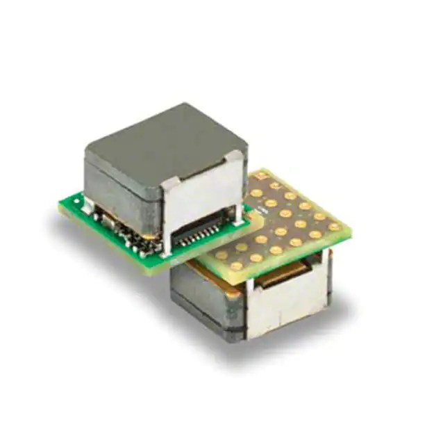


 工商网监
湘ICP备2023018690号
工商网监
湘ICP备2023018690号
