OKL-T/6-W12 Series
www.murata-ps.com
Programmable Output 6-Amp iLGA SMT PoLs
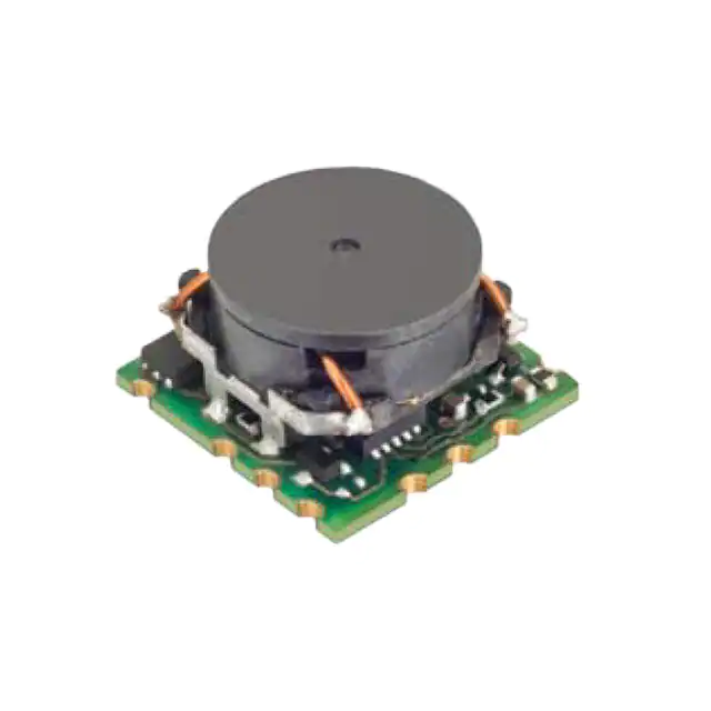
Typical unit
FEATURES
PRODUCT OVERVIEW
■
iLGA inspectable Land Grid Array
■
4.5-14Vdc input voltage range
■
Programmable output voltage from 0.591-5.5Vdc
■
Drives up to 300 μF ceramic capacitive loads
■
High power conversion efficiency at 93%
■
Outstanding thermal derating performance
■
Short circuit and over current protection
■
On/Off control and Power Good signal
■
Optional Sequence/Tracking operation (OKL2-T/6W12 models)
■
Certified to UL/EN/IEC 60950-1 safety, 2nd Edition
■
RoHS-6 hazardous substance compliance
The OKL-T/6-W12 series are miniature non-isolated Point-of-Load (PoL) DC/DC power converters
for embedded applications. Featuring inspectable
Land Grid Array (iLGA) format, the OKL-T/6-W12
measures only 0.48 x 0.48 x 0.283 inches max.
(12.2 x 12.2 x 7.2 mm max.).
The wide input range is 4.5 to 14 Volts DC.
The maximum output current is 6 Amps. Based
on fixed-frequency synchronous buck converter
switching topology, the high power conversion
efficient Point of Load (PoL) module features
programmable output voltage and On/Off control.
These converters also include under voltage lock
out (UVLO), output short circuit protection, and
over-current protections.
An optional sequence/tracking feature on
OKL2-T/6-W12 models allows power sequencing
of PoL’s. These units meet all standard UL/EN/IEC
60950-1 safety certifications (2nd Edition) and RoHS-6
hazardous substance compliance.
Connection Diagram
+Vin
F1
On/Off
Control
+Vout
t�4XJUDIJOH
Controller
Sense
t�'JMUFST
t�$VSSFOU�4FOTF
External
DC
Power
Source
Trim
Open = On
Closed = Off
(Positive
On/Off)
Reference and
Error Amplifier
Common
Sequence/Tracking
Common
Power Good out
Figure 1. OKL2-T/6-W12
Note: Murata Power Solutions strongly recommends an external input fuse, F1. See specifications.
For full details go to
www.murata-ps.com/rohs
www.murata-ps.com/support
MDC_OKL-T/6-W12 Series.C03 Page 1 of 17
�OKL-T/6-W12 Series
Programmable Output 6-Amp iLGA SMT PoLs
Model Number
Input
Efficiency
Regulation
(max.)
Vout
Iout (Amps, Power R/N (mV p-p)
Vin nom. Range Iin, no load Iin, full load
(Volts) ➀
max.)
(Watts)
Max. ➃
(Amps)
Line
Load (Volts) (Volts) ➀ (mA) ➃
Min. Typ.
OKL-T/6-W12P-C
0.591-5.5
6
30
20
±0.25% ±0.25%
12
4.5-14
20
2.69
91%
93%
Pos.
OKL-T/6-W12N-C
0.591-5.5
6
30
20
±0.25% ±0.25%
12
4.5-14
20
2.69
91%
93%
Neg.
OKL2-T/6-W12P-C
0.591-5.5
6
30
20
±0.25% ±0.25%
12
4.5-14
20
2.69
91%
93%
Pos.
OKL2-T/6-W12N-C
0.591-5.5
6
30
20
±0.25% ±0.25%
12
4.5-14
20
2.69
91%
93%
Neg.
Output
➀
➁
Seq/Track
On/Off Logic
PERFORMANCE SPECIFICATIONS SUMMARY AND ORDERING GUIDE
Package - Pinout P83
Case C83
inches (mm)
0.48x0.48x0.283 max
(12.2x12.2x7.2) max
0.48x0.48x0.283 max
no
(12.2x12.2x7.2) max
0.48x0.48x0.283 max
yes
(12.2x12.2x7.2) max
0.48x0.48x0.283 max
yes
(12.2x12.2x7.2) max
no
I/O caps are necessary for our test equipment and may not be needed for your application.
The output range is limited by Vin. See detailed specs.
All specifications are at nominal line voltage, Vout=nominal (5V) and full load, +25 deg.C.
unless otherwise noted.
➂ Use adequate ground plane and copper thickness adjacent to the converter.
Ripple and Noise (R/N) and no-load input current are shown at Vout=1V. See specs for details.
Output capacitors are 10 μF ceramic. Input cap is 22 μF. See detailed specifications.
PART NUMBER STRUCTURE
OK L 2 - T / 6 - W12 N - C
Non-isolated PoL
LGA Surface Mount
Sequence/tracking
Blank = Not installed
2 = Installed
RoHS Hazardous
Substance Compliance
C = RoHS-6 (does not claim EU RoHS exemption
7b–lead in solder)
Trimmable Output
Voltage Range
0.591-5.5Vdc
Maximum Rated Output
Current in Amps
On/Off Logic
P = Positive Logic
N = Negative Logic
Input Voltage Range
4.5-14Vdc
Product Label
Because of the small size of these products, the product label contains a
character-reduced code to indicate the model number and manufacturing date
code. Not all items on the label are always used. Please note that the label
differs from the product photograph. Here is the layout of the label:
Model Number
OKL-T/6-W12P-C
OKL-T/6-W12N-C
OKL2-T/6-W12P-C
OKL2-T/6-W12N-C
Product Code
L01106
L00106
L21106
L20106
The manufacturing date code is four characters:
Mfg.
date
code
XXXXXX
Product code
YMDX Rev.
Revision level
Figure 2. Label Artwork Layout
The label contains three rows of information:
First character – Last digit of manufacturing year, example 2009
Second character – Month code (1 through 9 = Jan-Sep;
O, N, D = Oct, Nov, Dec)
Third character – Day code (1 through 9 = 1 to 9, 10 = 0 and
11 through 31 = A through Z)
Fourth character – Manufacturing information
First row – Murata Power Solutions logo
Second row – Model number product code (see table)
Third row – Manufacturing date code and revision level
www.murata-ps.com/support
MDC_OKL-T/6-W12 Series.C03 Page 2 of 17
�OKL-T/6-W12 Series
Programmable Output 6-Amp iLGA SMT PoLs
Performance and Functional Specifications
See Note 1
Dynamic Characteristics
Input
Input Voltage Range
Isolation
Start-Up Voltage
Undervoltage Shutdown (see Note 15)
Overvoltage Shutdown
Reflected (Back) Ripple Current (Note 2)
Internal Input Filter Type
Recommended External Fuse
Reverse Polarity Protection
See Ordering Guide and Note 7.
Not isolated
4.2 V
3.4 V
None
TBD mA pk-pk
Capacitive
10A
None, install external fuse
Input Current:
Full Load Conditions
Inrush Transient
Shutdown Mode (Off, UV, OT)
Output in Short Circuit
Low Line (Vin=Vmin)
See Ordering Guide
TBD A2Sec.
1 mA
10 mA
4.54 A.
Remote On/Off Control (Note 5)
Negative Logic
Dynamic Load Response
Start-Up Time
(Vin on or On/Off to Vout regulated)
Switching Frequency
Current
Tracking/Sequencing (optional)
Slew Rate
Tracking accuracy, rising input
Tracking accuracy, falling input
Calculated MTBF (hours)
Telecordia method (4a)
Calculated MTBF (hours)
MIL-HDBK-217N2 method (4b)
Maximum Capacitive Loading (Note 14)
Cap-ESR=0.001 to 0.01 Ohms
Cap-ESR >0.01 Ohms
300 μF
1000 μF
Current Limit Inception (Note 6)
(98% of Vout setting, after warm up)
11 Amps
Short Circuit Mode
Short Circuit Current Output
Protection Method
Short Circuit Duration
Prebias Startup
Power Good output
PGood TRUE (HI)
PGood FALSE (LO)
10 mA
Hiccup autorecovery upon overload
removal. (Note 17)
Continuous, no damage
(output shorted to ground)
Converter will start up if the external
output voltage is less than Vnominal.
open drain configuration, 10 mA sink
(Vset -10%) < Vout < (Vset +10%)
0.0V < Vout < 0.4V
600 KHz
OKL Models
6,229,000
4,491,000
Relative Humidity
OKL2 Models
5,896,000
4,392,000
To 85%/+85 °C., non-condensing
Physical
Outline Dimensions
Weight
Plating Thickness
Safety
Output
30.45W max.
See Ordering Guide
No minimum load
±1.5 % of Vnominal
See Ordering Guide
None
TBD per °C of Vout range
See Ordering Guide and note 8
See Ordering Guide and note 10
See Ordering Guide
6 mSec for Vout=nominal (Vin On)
6 mSec for Vout=nominal (Remote On/Off)
Operating Temperature Range (Ambient, all output ranges)
See derating curves
-40 to TBD with derating (Note 9)
Storage Temperature Range
-55 to +125 °C.
Thermal Protection/Shutdown
Included in PWM
MSL Rating
2
See technical note on page 15
2 Volts per millisecond, max.
Vout = ±100 mV of Sequence In
Vout = ±100 mV of Sequence In
Output Power
Output Voltage Range
Minimum Loading
Accuracy (50% load, untrimmed)
Voltage Output Range (Note 13)
Overvoltage Protection (Note 16)
Temperature Coefficient
Ripple/Noise (20 MHz bandwidth)
Line/Load Regulation
Efficiency
(Note 1)
±450 mV
Environmental
ON = Open pin or -0.2V to +0.3V. max.
OFF = +3.5V min. to +Vin max.
ON = Open pin (internally pulled up) or
+3.5V to +Vin max.
OFF = -0.3V to +0.8V. max. or ground
1 mA max.
Positive Logic
50μSec max. to within ±2% of final value
(50-100% load step, di/dt=1A/µSec)
Peak Deviation
Restriction of Hazardous Substances
See Mechanical Specifications
0.06 ounces (1.6 grams)
Gold overplate 1.18μ" (0.03μm)
on Nickel subplate 118.1μ" (3.0μm)
Certified to UL/cUL 60950-1, CSAC22.2 No. 60950-1, IEC/EN 60950-1,
2nd Edition
RoHS-6 (does not claim EU RoHS exemption
7b–lead in solder)
Absolute Maximum Ratings
Input Voltage (Continuous or transient)
On/Off Control
Input Reverse Polarity Protection
Output Current (Note 7)
0 V. to +15 Volts max.
0 V. min. to +14V max.
None, install external fuse
Current-limited. Devices can withstand a
sustained short circuit without damage.
The outputs are not intended to accept
appreciable reverse current.
Storage Temperature
-55 to +125 °C.
Lead Temperature
See soldering specifications
Absolute maximums are stress ratings. Exposure of devices to greater than any of
any of these conditions may adversely affect long-term reliability. Proper operation
under conditions other than those listed in the Performance/Functional Specifications
Table is not implied nor recommended.
Specification Notes:
(1)
Specifications are typical at +25 °C, Vin=nominal (+12V.), Vout=nominal (+5V), full load, external caps and
natural convection unless otherwise indicated. Extended tests at full power must supply substantial forced
airflow.
All models are tested and specified with external 10μF ceramic output capacitors and a 22 μF external
input capacitor. All capacitors are low ESR types. These capacitors are necessary to accommodate our test
equipment and may not be required to achieve specified performance in your applications. However, Murata
Power Solutions recommends installation of these capacitors. All models are stable and regulate within
spec under no-load conditions.
(2)
Input Back Ripple Current is tested and specified over a 5 Hz to 20 MHz bandwidth. Input filtering is Cin=2 x
100 μF ceramic, Cbus=1000 μF electrolytic, Lbus=1 μH.
(3)
Note that Maximum Power Derating curves indicate an average current at nominal input voltage. At higher
temperatures and/or lower airflow, the DC/DC converter will tolerate brief full current outputs if the total
RMS current over time does not exceed the Derating curve.
www.murata-ps.com/support
MDC_OKL-T/6-W12 Series.C03 Page 3 of 17
�OKL-T/6-W12 Series
Programmable Output 6-Amp iLGA SMT PoLs
Specification Notes, Cont.:
(4a) Mean Time Before Failure is calculated using the Telcordia (Belcore) SR-332 Method 1, Case 3, ground fixed
conditions, Tpcboard=+25 ˚C, full output load, natural air convection.
(12) Maximum PC board temperature is measured with the sensor in the center of the converter.
(4b) Mean Time Before Failure is calculated using the MIL-HDBK-217N2 method, ground benign, +25ºC., full output
load, natural convection.
(14) The maximum output capacitive loads depend on the the Equivalent Series Resistance (ESR) of the external
output capacitor and, to a lesser extent, the distance and series impedance to the load. Larger caps will reduce
output noise but may change the transient response. Newer ceramic caps with very low ESR may require lower
capacitor values to avoid instability. Thoroughly test your capacitors in the application. Please refer to the Output
Capacitive Load Application Note.
(5)
The On/Off Control Input should use either a switch or an open collector/open drain transistor referenced to
-Input Common. A logic gate may also be used by applying appropriate external voltages which do not exceed
+Vin.
(6)
Short circuit shutdown begins when the output voltage degrades approximately 2% from the selected setting.
(7)
Please observe the voltage input and output specifications in the Voltage Range Graph on page 17.
(8)
Output noise may be further reduced by adding an external filter. At zero output current, the output may contain
low frequency components which exceed the ripple specification. The output may be operated indefinitely with
no load.
(9)
All models are fully operational and meet published specifications, including “cold start” at –40˚ C.
(10) Regulation specifications describe the deviation as the line input voltage or output load current is varied from a
nominal midpoint value to either extreme.
(13) Do not exceed maximum power specifications when adjusting the output trim.
(15) Do not allow the input voltage to degrade lower than the input undervoltage shutdown voltage at all times.
Otherwise, you risk having the converter turn off. The undervoltage shutdown is not latching and will attempt to
recover when the input is brought back into normal operating range.
(16) The outputs are not intended to sink appreciable reverse current.
(17) “Hiccup” overcurrent operation repeatedly attempts to restart the converter with a brief, full-current output. If the
overcurrent condition still exists, the restart current will be removed and then tried again. This short current pulse
prevents overheating and damaging the converter. Once the fault is removed, the converter immediately recovers
normal operation.
(11) Other input or output voltage ranges will be reviewed under scheduled quantity special order.
www.murata-ps.com/support
MDC_OKL-T/6-W12 Series.C03 Page 4 of 17
�OKL-T/6-W12 Series
Programmable Output 6-Amp iLGA SMT PoLs
PERFORMANCE DATA AND OSCILLOGRAMS
Efficiency vs. Line Voltage and Load Current @ +25˚C. (Vout = 5.0V)
Maximum Current Temperature Derating at Sea Level (Vin=12V, Vout=5.0V)
100
7
6
95
Output Current (Amps)
Efficiency (%)
5
90
VIN = 6.5V
VIN = 12V
VIN = 14V
85
Natural Convection
65 LFM
100 LFM
4
3
2
80
1
75
0
1
2
3
4
Load Curre nt (Amps)
5
6
0
20
25
30
35
40
45
50
55
60
65
Ambient Temperature (ºC)
70
75
80
85
90
On/Off Enable Delay (Vin=12V, Vout=5.0V, Iout=6A, Cload=0)
Trace 4=Enable, Trace2=Vout
Output Ripple and Noise (Vin=12V, Vout=5.0V, Iout=6A, Cload=0, ScopeBW=20MHz)
Step Load Transient Response (Vin=12V, Vout=5.0V, Cload=0, Iout=3A to 6A)
Trace 2=Vout, 200 mV/div. Trace 4=Iout, 5A/div.
Step Load Transient Response (Vin=12V, Vout=5.0V, Cload=0, Iout=6A to 3A)
Trace 2=Vout, 200 mV/div. Trace 4=Iout, 5A/div.
www.murata-ps.com/support
MDC_OKL-T/6-W12 Series.C03 Page 5 of 17
�OKL-T/6-W12 Series
Programmable Output 6-Amp iLGA SMT PoLs
PERFORMANCE DATA AND OSCILLOGRAMS
Efficiency vs. Line Voltage and Load Current @ +25˚C. (Vout = 3.3V)
Maximum Current Temperature Derating at Sea Level (Vin=12V, Vout=3.3V)
100
7
6
95
Output Current (Amps)
Efficiency (%)
5
90
VIN = 4.5V
VIN = 12V
VIN = 14V
85
Natural Convection
65 LFM
100 LFM
4
3
2
80
1
75
0
1
2
3
4
Load Curre nt (Amps)
5
6
0
20
25
30
35
40
45
50
55
60
65
70
75
80
85
90
Ambient Temperature (ºC)
On/Off Enable Delay (Vin=12V, Vout=3.3V, Iout=6A, Cload=0)
Trace 4=Enable, Trace2=Vout
Output Ripple and Noise (Vin=12V, Vout=3.3V, Iout=6A, Cload=0, ScopeBW=20MHz)
Step Load Transient Response (Vin=12V, Vout=3.3V, Cload=0, Iout=3A to 6A)
Trace 2=Vout, 200 mV/div. Trace 4=Iout, 5A/div.
Step Load Transient Response (Vin=12V, Vout=3.3V, Cload=0, Iout=6A to 3A)
Trace 2=Vout, 200 mV/div. Trace 4=Iout, 5A/div.
www.murata-ps.com/support
MDC_OKL-T/6-W12 Series.C03 Page 6 of 17
�OKL-T/6-W12 Series
Programmable Output 6-Amp iLGA SMT PoLs
PERFORMANCE DATA AND OSCILLOGRAMS
Efficiency vs. Line Voltage and Load Current @ +25˚C. (Vout = 2.5V)
Maximum Current Temperature Derating at Sea Level (Vin=12V, Vout=2.5V)
100
7
6
95
Output Current (Amps)
Efficiency (%)
5
90
VIN = 4.5V
VIN = 12V
VIN = 14V
85
Natural Convection
65 LFM
100 LFM
4
3
2
80
1
75
0
1
2
3
4
Load Curre nt (Amps)
5
6
0
20
25
30
35
40
45
50
55
60
65
70
75
80
85
90
Ambient Temperature (ºC)
On/Off Enable Delay (Vin=12V, Vout=2.5V, Iout=6A, Cload=0)
Trace 4=Enable, Trace2=Vout
Output Ripple and Noise (Vin=12V, Vout=2.5V, Iout=6A, Cload=0, ScopeBW=20MHz)
Step Load Transient Response (Vin=12V, Vout=2.5V, Cload=0, Iout=3A to 6A)
Trace 2=Vout, 200 mV/div. Trace 4=Iout, 5A/div.
Step Load Transient Response (Vin=12V, Vout=2.5V, Cload=0, Iout=6A to 3A)
Trace 2=Vout, 200 mV/div. Trace 4=Iout, 5A/div.
www.murata-ps.com/support
MDC_OKL-T/6-W12 Series.C03 Page 7 of 17
�OKL-T/6-W12 Series
Programmable Output 6-Amp iLGA SMT PoLs
PERFORMANCE DATA AND OSCILLOGRAMS
Efficiency vs. Line Voltage and Load Current @ +25˚C. (Vout = 1.8V)
Maximum Current Temperature Derating at Sea Level (Vin=12V, Vout=1.8V)
100
7
6
95
Output Current (Amps)
Efficiency (%)
5
90
VIN = 4.5V
VIN = 12V
VIN = 14V
85
Natural Convection
65 LFM
100 LFM
4
3
2
80
1
75
0
1
2
3
4
Load Curre nt (Amps)
5
6
0
20
25
30
35
40
45
50
55
60
65
70
75
80
85
90
Ambient Temperature (ºC)
On/Off Enable Delay (Vin=12V, Vout=1.8V, Iout=6A, Cload=0)
Trace 4=Enable, Trace2=Vout
Output Ripple and Noise (Vin=12V, Vout=1.8V, Iout=6A, Cload=0, ScopeBW=20MHz)
Step Load Transient Response (Vin=12V, Vout=1.8V, Cload=0, Iout=3A to 6A)
Trace 2=Vout, 200 mV/div. Trace 4=Iout, 5A/div.
Step Load Transient Response (Vin=12V, Vout=1.8V, Cload=0, Iout=6A to 3A)
Trace 2=Vout, 200 mV/div. Trace 4=Iout, 5A/div.
www.murata-ps.com/support
MDC_OKL-T/6-W12 Series.C03 Page 8 of 17
�OKL-T/6-W12 Series
Programmable Output 6-Amp iLGA SMT PoLs
PERFORMANCE DATA AND OSCILLOGRAMS
Maximum Current Temperature Derating at Sea Level (Vin=12V, Vout=1.2V)
100
7
95
6
90
5
Output Current (Amps)
Efficiency (%)
Efficiency vs. Line Voltage and Load Current @ +25˚C. (Vout = 1.2V)
85
80
VIN = 4.5V
VIN = 12V
VIN = 14V
75
Natural Convection
65 LFM
100 LFM
4
3
2
70
1
65
0
1
2
3
4
Load Curre nt (Amps)
5
6
0
20
25
30
35
40
45
50
55
60
65
Ambient Temperature (ºC)
70
75
80
85
90
On/Off Enable Delay (Vin=12V, Vout=1.2V, Iout=6A, Cload=0)
Trace 4=Enable, Trace2=Vout
Output Ripple and Noise (Vin=12V, Vout=1.2V, Iout=6A, Cload=0, ScopeBW=20MHz)
Step Load Transient Response (Vin=12V, Vout=1.2V, Cload=0, Iout=3A to 6A)
Trace 2=Vout, 200 mV/div. Trace 4=Iout, 5A/div.
Step Load Transient Response (Vin=12V, Vout=1.2V, Cload=0, Iout=6A to 3A)
Trace 2=Vout, 200 mV/div. Trace 4=Iout, 5A/div.
www.murata-ps.com/support
MDC_OKL-T/6-W12 Series.C03 Page 9 of 17
�OKL-T/6-W12 Series
Programmable Output 6-Amp iLGA SMT PoLs
PERFORMANCE DATA AND OSCILLOGRAMS
Efficiency vs. Line Voltage and Load Current @ +25˚C. (Vout = 1.0V)
Maximum Current Temperature Derating at Sea Level (Vin=12V, Vout=1.0V)
100
7
95
6
90
Output Current (Amps)
Efficiency (%)
5
85
80
VIN = 4.5V
VIN = 12V
VIN = 14V
75
3
70
2
65
1
60
0
1
2
3
4
Load Curre nt (Amps)
5
6
Natural Convection
65 LFM
100 LFM
4
0
20
25
30
35
40
45
50
55
60
65
70
75
80
85
90
Ambient Temperature (ºC)
On/Off Enable Delay (Vin=12V, Vout=1.0V, Iout=6A, Cload=0)
Trace 4=Enable, Trace2=Vout
Output Ripple and Noise (Vin=12V, Vout=1.0V, Iout=6A, Cload=0, ScopeBW=20MHz)
Step Load Transient Response (Vin=12V, Vout=1.0V, Cload=0, Iout=3A to 6A)
Trace 2=Vout, 200 mV/div. Trace 4=Iout, 5A/div.
Step Load Transient Response (Vin=12V, Vout=1.0V, Cload=0, Iout=6A to 3A)
Trace 2=Vout, 200 mV/div. Trace 4=Iout, 5A/div.
www.murata-ps.com/support
MDC_OKL-T/6-W12 Series.C03 Page 10 of 17
�OKL-T/6-W12 Series
Programmable Output 6-Amp iLGA SMT PoLs
MECHANICAL SPECIFICATIONS
Top View
INPUT/OUTPUT CONNECTIONS
0.48
(12.19)
Pin
1
2
3
4
5
6
7
8
9
10
11
12
Bottom View
0.48
(12.19)
Side View
Function
On/Off Control*
VIN
Ground
VOUT
Sense
Trim
Ground
No Connection
Sequence/Tracking**
Power Good Out
No Connection
No Connection
*The Remote On/Off can be provided with
either positive (P suffix) or negative (N
suffix) logic.
**OKL2 models only
0.283
(7.2)
max.
SOLDER PAD NOTES:
[1] To avoid incorrect contacts with exposed via’s and plated through holes on the bottom of the converter, do not have any
exposed copper around the unit aside from our recommended footprint. Except for connections to the pads, keep all external
circuits away from the board edges.
[2] Do not connect any additional components between the Trim pin and Vout or between the Trim and Sense pins. Use only
the specified connections.
End View
Recommended Footprint
-through the Board-
3
4
12.7
0.50
0.375 (9.53)
0.195 (4.95)
0
0.060 (1.52)
Bottom View
3.43
0.135
2
0.070-0.080 [1.78-2.03mm]
x
0.160-0.170 [4.06-4.32mm]
3 PLACES
1.27
0.050 (14 PLS)
4.57
0.180
2
3
Vin
Gnd
1.14
0.045
4
0.240 (6.10)
Gnd
Vout
0.375 (9.53)
5
Sense
11
Trim
NC
4.57
0.180
On/Off
NC
0.150 (3.81)
6
Vin
Gnd
1
PGood
NC Seq
0.060 (1.52)
10
2.29
0.090 10
Sense
On/Off
PG
NC
NC
Gnd NC
8
7
Trim1
9
5
3.43
0.135
12.40
0.488
CL
11
4.57
0.180
6
9 Seq
8
0.040-0.050 [1.02-1.27mm]
SQUARE PAD (9 PLS)
4.57
0.180
Plating Thickness:
Gold overplate 1.18μ" (0.03μm)
on Nickel subplate 118.1μ" (3.0μm)
CL
12.40
0.488
Tolerances (unless otherwise specified):
.XX ± 0.02 (0.5)
.XXX ± 0.010 (0.25)
Angles ± 1˚
Components are shown for reference only.
12
2.29
0.090
0.420 (10.67)
7
0.330 (8.38)
Dimensions are in inches (mm shown for ref. only).
0.150 (3.81)
12
0.240 (6.10)
0
Third Angle Projection
12.7
0.50
1
Vout1
0.420 (10.67)
2.29
0.090
Copper Pads
No Exposed
Copper
Permitted
Figure 3. OKL-T/6-W12 Mechanical Outline
www.murata-ps.com/support
MDC_OKL-T/6-W12 Series.C03 Page 11 of 17
�OKL-T/6-W12 Series
Programmable Output 6-Amp iLGA SMT PoLs
TAPE AND REEL INFORMATION (MSL RATING 2)
Tape Detail
7.40±0.1
A’
B-B’ SECTION
12.60±0.1
L00103
B
A
YMDX Rev.
L00103
YMDX Rev.
L00103
YMDX Rev.
Vacuum Pickup
Point in Center
0.40±0.05
(7.0º)
4.00±0.1
24.00+0.3
-0.1
16.00±0.1
B’
11.50±0.1
ø1.50+0.1
-0
1.75±0.1
Round
Sprocket
Holes
2.00±0.1
Pulling direction
12.60±0.1
(7.0º)
Notes
1) The radius (R) is 0.3mm max.
2) Cumulative tolerance of 10 pitches of the sprocket hole is ±0.2mm.
A-A’ SECTION
Reel Detail
Reel diameter 330.2
Start of
pocket tape
A
End of modules
C
B
Start of
modules
in pockets
Hub diameter 13.00
Start of
cover tape
Inner diameter 101.6
All dimensions are in millimeters.
Reel Information (400 units per reel)
Key
Description
Length (mm)
A
Tape trailer (no modules)
800 ±40
B
Pocket tape length before modules
200 min.
C
Cover tape length before pocket tape
240 ±40
www.murata-ps.com/support
MDC_OKL-T/6-W12 Series.C03 Page 12 of 17
�OKL-T/6-W12 Series
Programmable Output 6-Amp iLGA SMT PoLs
TECHNICAL NOTES
Output Voltage Adustment
The output voltage may be adjusted over a limited range by connecting an
external trim resistor (Rtrim) between the Trim pin and Ground. The Rtrim
is recommended to have a ±0.5% accuracy (or better) with low temperature coefficient, ±100 ppm/°C or better. Mount the resistor close to the
converter with very short leads or use a surface mount trim resistor.
In the tables below, the calculated resistance is given. Do not exceed the
specified limits of the output voltage or the converter’s maximum power rating
when applying these resistors. Also, avoid high noise at the Trim input. However,
to prevent instability, you should never connect any capacitors to Trim.
OKL-T/6-W12
Output Voltage
Calculated Rtrim (KΩ)
5.0 V.
1.34
3.3 V.
2.18
2.5 V.
3.1
2.0 V.
4.19
1.8 V.
4.88
1.5 V.
6.50
1.2 V.
9.70
1.0 V.
14.45
0.591 V.
∞ (open)
Resistor Trim Equation, OKL-T/6-W12 models:
5.91
RTRIM (k) = _____________
VOUT – 0.591
Do not connect any additional components between the Vtrim pin and Vout
or between the Trim and Sense pins. Use only the specified connections as
recommended per this data sheet.
Input Fusing
Certain applications and/or safety agencies may require fuses at the inputs
of power conversion components. Fuses should also be used when there
is the possibility of sustained input voltage reversal which is not currentlimited. For greatest safety, we recommend a fast blow fuse installed in the
ungrounded input supply line.
The installer must observe all relevant safety standards and regulations.
For safety agency approvals, install the converter in compliance with the
end-user safety standard.
Input Under-Voltage Shutdown and Start-Up Threshold
Under normal start-up conditions, converters will not begin to regulate
properly until the ramping-up input voltage exceeds and remains at the
Start-Up Threshold Voltage (see Specifications). Once operating, converters will not turn off until the input voltage drops below the Under-Voltage
Shutdown Limit. Subsequent restart will not occur until the input voltage
rises again above the Start-Up Threshold. This built-in hysteresis prevents
any unstable on/off operation at a single input voltage.
Users should be aware however of input sources near the Under-Voltage
Shutdown whose voltage decays as input current is consumed (such as
capacitor inputs), the converter shuts off and then restarts as the external
capacitor recharges. Such situations could oscillate. To prevent this, make
sure the operating input voltage is well above the UV Shutdown voltage AT
ALL TIMES.
Start-Up Time
Assuming that the output current is set at the rated maximum, the Vin to
Vout Start-Up Time (see Specifications) is the time interval between the
point when the ramping input voltage crosses the Start-Up Threshold and
the fully loaded regulated output voltage enters and remains within its
specified accuracy band. Actual measured times will vary with input source
impedance, external input capacitance, input voltage slew rate and final
value of the input voltage as it appears at the converter.
These converters include a soft start circuit to moderate the duty cycle of
its PWM controller at power up, thereby limiting the input inrush current.
The On/Off Remote Control interval from On command to Vout regulated
assumes that the converter already has its input voltage stabilized above the
Start-Up Threshold before the On command. The interval is measured from the
On command until the output enters and remains within its specified accuracy
band. The specification assumes that the output is fully loaded at maximum
rated current. Similar conditions apply to the On to Vout regulated specification
such as external load capacitance and soft start circuitry.
Recommended Input Filtering
The user must assure that the input source has low AC impedance to
provide dynamic stability and that the input supply has little or no inductive
content, including long distributed wiring to a remote power supply. The
converter will operate with no additional external capacitance if these
conditions are met.
For best performance, we recommend installing a low-ESR capacitor
immediately adjacent to the converter’s input terminals. The capacitor should
be a ceramic type such as the Murata GRM32 series or a polymer type. Initial
suggested capacitor values are 10 to 22 μF, rated at twice the expected
maximum input voltage. Make sure that the input terminals do not go below the
undervoltage shutdown voltage at all times. More input bulk capacitance may
be added in parallel (either electrolytic or tantalum) if needed.
Recommended Output Filtering
The converter will achieve its rated output ripple and noise with no
additional external capacitor. However, the user may install more external output capacitance to reduce the ripple even further or for improved
dynamic response. Again, use low-ESR ceramic (Murata GRM32 series)
or polymer capacitors. Initial values of 10 to 47 μF may be tried, either
single or multiple capacitors in parallel. Mount these close to the converter.
Measure the output ripple under your load conditions.
Use only as much capacitance as required to achieve your ripple and
noise objectives. Excessive capacitance can make step load recovery
sluggish or possibly introduce instability. Do not exceed the maximum rated
output capacitance listed in the specifications.
Input Ripple Current and Output Noise
All models in this converter series are tested and specified for input
reflected ripple current and output noise using designated external input/
output components, circuits and layout as shown in the figures below. The
Cbus and Lbus components simulate a typical DC voltage bus. Please note
that the values of Cin, Lbus and Cbus will vary according to the specific
converter model.
www.murata-ps.com/support
MDC_OKL-T/6-W12 Series.C03 Page 13 of 17
�OKL-T/6-W12 Series
Programmable Output 6-Amp iLGA SMT PoLs
TO
OSCILLOSCOPE
CURRENT
PROBE
+VIN
VIN
+
–
+
–
LBUS
CBUS
+VOUT
CIN
C1
-VIN
CIN = 2 x 100μF, ESR < 700mΩ @ 100kHz
CBUS = 1000μF, ESR < 100mΩ @ 100kHz
LBUS = 1μH
Figure 4: Measuring Input Ripple Current
C2
SCOPE
RLOAD
-VOUT
C1 = 1μF
C2 = 10μF
LOAD 2-3 INCHES (51-76mm) FROM MODULE
Figure 5: Measuring Output Ripple and Noise (PARD)
Minimum Output Loading Requirements
All models regulate within specification and are stable under no load to full
load conditions. Operation under no load might however slightly increase
output ripple and noise.
Thermal Shutdown
To prevent many over temperature problems and damage, these converters
include thermal shutdown circuitry. If environmental conditions cause the
temperature of the DC/DC’s to rise above the Operating Temperature Range
up to the shutdown temperature, an on-board electronic temperature
sensor will power down the unit. When the temperature decreases below
the turn-on threshold, the converter will automatically restart. There is a
small amount of hysteresis to prevent rapid on/off cycling.
CAUTION: If you operate too close to the thermal limits, the converter
may shut down suddenly without warning. Be sure to thoroughly test your
application to avoid unplanned thermal shutdown.
Temperature Derating Curves
The graphs in this data sheet illustrate typical operation under a variety of
conditions. The Derating curves show the maximum continuous ambient air
temperature and decreasing maximum output current which is acceptable under increasing forced airflow measured in Linear Feet per Minute
(“LFM”). Note that these are AVERAGE measurements. The converter will
accept brief increases in current or reduced airflow as long as the average
is not exceeded.
Note that the temperatures are of the ambient airflow, not the converter
itself which is obviously running at higher temperature than the outside
air. Also note that very low flow rates (below about 25 LFM) are similar to
“natural convection”, that is, not using fan-forced airflow.
Murata Power Solutions makes Characterization measurements in a
closed cycle wind tunnel with calibrated airflow. We use both thermocouples and an infrared camera system to observe thermal performance.
CAUTION: These graphs are all collected at slightly above Sea Level
altitude. Be sure to reduce the derating for higher density altitude.
Output Voltage Sequencing
The OKL modules include a sequencing feature that enables users to
implement various types of output voltage sequencing in their applications.
This is accomplished via an additional sequencing pin. When not using the
sequencing feature, either tie the sequence pin to Vin or leave it unconnected.
When an analog voltage is applied to the sequence pin, the output
voltage tracks this voltage until the output reaches the set-point voltage.
The final value of the sequence voltage must be set higher than the setpoint voltage of the module. The output voltage follows the voltage on the
sequence pin on a one-to-one volt basis. By connecting multiple modules
together, multiple modules can track their output voltages to the voltage
applied on the sequence pin.
For proper voltage sequencing, first, input voltage is applied to the
module. The On/Off pin of the module is left unconnected (or tied to GND
for negative logic modules or tied to Vin for positive logic modules) so that
the module is ON by default. After applying input voltage to the module,
a minimum 10msec delay is required before applying voltage on the
sequence pin. During this time, a voltage of 50mV (± 20 mV) is maintained
on the sequence pin. This delay gives the module enough time to complete
its internal powerup soft-start cycle. During the delay time, the sequence
pin should be held close to ground (nominally 50mV ± 20 mV). This is required to keep the internal opamp out of saturation thus preventing output
overshoot during the start of the sequencing ramp. By selecting resistor R1
according to the following equation
23500
R1 = ———— ohms,
Vin – 0.05
the voltage at the sequencing pin will be 50mV when the sequencing
signal is at zero. See figure 6 for R1 connection for the sequencing signal to
the SEQ pin.
http://www.murata-ps.com/data/apnotes/dcan-61.pdf
Click here to view Application Note DCAN-61
www.murata-ps.com/support
MDC_OKL-T/6-W12 Series.C03 Page 14 of 17
�OKL-T/6-W12 Series
Programmable Output 6-Amp iLGA SMT PoLs
Output Current Limiting
Current limiting inception is defined as the point at which full power falls
below the rated tolerance. See the Performance/Functional Specifications. Note particularly that the output current may briefly rise above its
rated value in normal operation as long as the average output power is
not exceeded. This enhances reliability and continued operation of your
application. If the output current is too high, the converter will enter the
short circuit condition.
Output Capacitive Load
These converters do not require external capacitance added to achieve
rated specifications. Users should only consider adding capacitance to
reduce switching noise and/or to handle spike current load steps. Install
only enough capacitance to achieve noise objectives. Excess external
capacitance may cause regulation problems, degraded transient response
and possible oscillation or instability.
Output Short Circuit Condition
When a converter is in current-limit mode, the output voltage will drop
as the output current demand increases. Following a time-out period, the
PWM will restart, causing the output voltage to begin ramping up to its
appropriate value. If the short-circuit condition persists, another shutdown
cycle will initiate. This rapid on/off cycling is called “hiccup mode”. The
hiccup cycling reduces the average output current, thereby preventing
excessive internal temperatures and/or component damage. A short circuit
can be tolerated indefinitely.
The “hiccup” system differs from older latching short circuit systems
because you do not have to power down the converter to make it restart.
The system will automatically restore operation as soon as the short circuit
condition is removed.
Remote On/Off Control
The OKL Series power modules can be specifi ed with either a positive or negative logic type. See Figures 7 and 8 for On/Off circuit control. In the positive
logic on/off option the unit turns on during a logic high on the On/Off pin and
turns off during a logic low. In a negative logic on/off option, the unit turns off
during logic high and on during logic low. The On/Off signal should always be
reference to ground. For positive or negative option, leaving then On/Off pin
disconnected will turn the unit on when input voltage is present.
Positive—Units are enabled when the on/off pin is left open or is pulled
high to +Vin. The On/Off circuit control is shown in fi gure 7. When the
external transistor Q1 is in the off state, the internal PWM enable pin is pull
high causing the unit to turn on. When Q1 is turn on, the On/Off pin is
pulled low and the units is off. Rp should be around 20K ohms.
Negative—Units are enabled when the ON/Off is open or brought to
within a low voltage (see specifi cations) with respect to –Vin. The unit is
off when the ON/Off is pulled high with respect to –Vin (see specifi cations).
The On/Off circuitry is shown in fi gure 8. The On/Off pin should be pulled
high with an external pull-up resistor (20K ohms). When Q1 is in the off
state, the On/Off pin is pulled high, transistor Q3 is turn on and the unit is
off. To turn on the unit, Q1 is turn on, pulling the On/Off pin low and turning
Q3 off resulting on the unit being on.
Dynamic control of the On/Off function should be able to sink the speci-fi
ed signal current when brought low and withstand appropriate voltage
when brought high. Be aware too that there is a fi nite time in milliseconds
(see specifi cations) between the time of On/Off Control activation and
stable, regulated output. This time will vary slightly with output load type
and current and input conditions.
OKL -T
+Vin
470K
+
OUT
R1
–
SEQ
Control Voltage
10K
SEQ
GND
Figure 6. Sequencing Signal Interface of Module
OKL N Module
+Vin
+Vin
E
PWM
Rp
On/Off
Q3
GND
Q1
GND
GND
BOM Rp 20K
BOM Q1 Q SMT MOS P 30V
Figure 7. On/Off Circuit Control for Using Negative On/Off Logic
www.murata-ps.com/support
MDC_OKL-T/6-W12 Series.C03 Page 15 of 17
�OKL-T/6-W12 Series
Programmable Output 6-Amp iLGA SMT PoLs
Voltage Range Graph
Please observe the limits below for voltage input and output ranges. These
limits apply at all output currents.
16
14
Soldering Guidelines
Murata Power Solutions recommends the specifications below when installing these
converters. These specifications vary depending on the solder type. Exceeding these
specifications may cause damage to the product. Your production environment may differ
therefore please thoroughly review these guidelines with your process engineers.
Input Voltage (V)
12
Reflow Solder Operations for surface-mount products (SMT)
10
For Sn/Ag/Cu based solders:
Vin=14V / Vout=1V
8
Preheat Temperature
Less than 1 ºC. per second
6
Time over Liquidus
45 to 75 seconds
4
Maximum Peak Temperature
260 ºC.
Cooling Rate
Less than 3 ºC. per second
Vin=4.5V / Vout=3.63V
Upper Limit
Lower Limit
2
For Sn/Pb based solders:
0
0.5
1
1.5
2
2.5
3
3.5
Output Voltage (V)
4
4.5
5
5.5
Preheat Temperature
Less than 1 ºC. per second
Time over Liquidus
60 to 75 seconds
Maximum Peak Temperature
235 ºC.
Cooling Rate
Less than 3 ºC. per second
Recommended Lead-free Solder Reflow Profile
Peak Temp.
235-260° C
250
Temperature (°C)
200
Reflow Zone
150
Soaking Zone
time above 217° C
45-75 sec
120 sec max
100


 工商网监
湘ICP备2023018690号
工商网监
湘ICP备2023018690号
