WT11
D a t a
S h e e t
V e r s i o n
F r i d a y ,
3 . 1
M a y
2 2 ,
2 0 0 9
�Copyright © 2000-2009 Bluegiga Technologies
All rights reserved.
Bluegiga Technologies assumes no responsibility for any errors, which may appear in this manual.
Furthermore, Bluegiga Technologies reserves the right to alter the hardware, software, and/or
specifications detailed herein at any time without notice, and does not make any commitment to
update the information contained herein. Bluegiga Technologies’ products are not authorized for use
as critical components in life support devices or systems.
The WRAP is a registered trademark of Bluegiga Technologies
The Bluetooth trademark is owned by the Bluetooth SIG Inc., USA, and is licensed to Bluegiga
Technologies.
All other trademarks listed herein are owned by their respective owners.
�Contents:
1.
Block Diagram and Descriptions ........................................................6
2.
Electrical characteristics ....................................................................9
3.
WT11 pin description .......................................................................13
4.
Physical Interfaces ..........................................................................16
4.1
UART Interface.......................................................................................... 16
4.1.1
UART Configuration While RESET is Active ............................................... 17
4.1.2
UART Bypass Mode............................................................................... 17
4.2
USB Interface ........................................................................................... 19
4.2.1
USB Pull-Up Resistor ............................................................................ 19
4.2.2
Self Powered Mode ............................................................................... 19
4.2.3
Bus Powered Mode ............................................................................... 20
4.2.4
Suspend Current .................................................................................. 21
4.2.5
Detach and Wake-Up Signaling .............................................................. 21
4.2.6
USB Driver .......................................................................................... 22
4.2.7
USB 1.1 Compliance ............................................................................. 22
4.2.8
USB 2.0 Compatibility ........................................................................... 22
4.3
SPI Interface ............................................................................................ 23
4.4
PCM Interface ........................................................................................... 24
4.4.1
PCM Interface Master/Slave ................................................................... 24
4.4.2
Long Frame Sync ................................................................................. 25
4.4.3
Short Frame Sync ................................................................................ 25
4.4.4
Multi Slot Operation.............................................................................. 26
4.4.5
GCI Interface ...................................................................................... 26
4.4.6
Slots and Sample Formats ..................................................................... 27
4.4.7
Additional Features .............................................................................. 28
4.4.8
PCM Configuration ................................................................................ 28
5.
I/O Parallel Ports ............................................................................30
6.
Software Stacks ...............................................................................31
2
�6.1
iWRAP Stack ............................................................................................. 31
6.2
HCI Stack ................................................................................................. 32
6.3
RFCOMM Stack .......................................................................................... 35
6.4
VM Stack .................................................................................................. 36
6.5
HID Stack ................................................................................................ 37
7.
Enhanced Data Rate .........................................................................39
7.1
Enhanced Data Rate Baseband .................................................................... 39
7.2
Enhanced Data Rate /4 DQPSK .................................................................. 39
7.3
8DQPSK ................................................................................................... 39
8.
Layout and Soldering Considerations ...............................................41
8.1
Soldering recommendations ........................................................................ 41
8.2
Layout guidelines ...................................................................................... 41
9.
WT11 physical dimensions ...............................................................43
10. Package ...........................................................................................46
11. Certifications ...................................................................................48
11.1
Bluetooth ............................................................................................ 48
11.2
FCC.................................................................................................... 49
11.2.1
FCC antenna designation .................................................................... 50
11.3
CE ..................................................................................................... 51
11.4
Industry Canada (IC)............................................................................ 51
12. RoHS Statement with a List of Banned Materials .............................52
13. Contact Information ........................................................................53
3
�TERMS & ABBREVIATIONS
Term or Abbreviation:
Explanation:
Bluetooth
Set of technologies providing audio and data transfer over short-range
radio connections
CE
Conformité Européene
DFU
Device Firmware Upgrade
EDR
Enhanced Data Rate
FCC
Federal Communications Commission
HCI
Host Controller Interface
HID
Human Interface Device
iWRAP
Interface for WRAP
PCB
Printed Circuit Board
PCM
Pulse Code Modulation
RoHS
The Restriction of Hazardous Substances in Electrical and Electronic
Equipment Directive (2002/95/EC)
SPI
Serial Peripheral Interface
UART
Universal Asynchronous Transmitter Receiver
USB
Universal Serial Bus
VM
Virtual Machine
WRAP
Wireless Remote Access Platform
4
�WT11 Bluetoooth
module
DESCRIPTION
FEATURES:
WT11 is a next-generation, class 1,
Bluetooth® 2.0+EDR (Enhanced Data Rates)
module. It introduces three times faster data
rates compared to existing Bluetooth® 1.2
modules even with lower power consumption!
WT11 is a highly integrated and sophisticated
Bluetooth® module, containing all the
necessary elements from Bluetooth® radio to
antenna and a fully implemented protocol
stack. Therefore WT11 provides an ideal
solution for developers who want to integrate
Bluetooth® wireless technology into their
design with limited knowledge of Bluetooth®
and RF technologies.
By default WT11 module is equipped with
powerful and easy-to-use iWRAP firmware.
iWRAP enables users to access Bluetooth®
functionality with simple ASCII commands
delivered to the module over serial interface it's just like a luetooth® modem.
Fully Qualified Bluetooth system v2.0 +
EDR, CE and FCC
Class 1, range up to 300 meters
Integrated chip antenna or UFL connector
Industrial temperature range from -40oC
to +85oC
Enhanced Data Rate (EDR) compliant with
v2.0.E.2 of specification for both 2Mbps
and 3Mbps modulation modes
RoHS Compliant
Full Speed Bluetooth Operation with Full
Piconet
Scatternet Support
USB interface (USB 2.0 compatible)
UART with bypass mode
Support for 802.11 Coexistence
8Mbits of Flash Memory
APPLICATIONS:
Hand held terminals
Industrial devices
Point-of-Sale systems
PCs
Personal Digital Assistants (PDAs)
Computer Accessories
Access Points
Automotive Diagnostics Units
Figure 1: Physical outlook of WT11-A
Figure 2: Physical outlook of WT11-E
ORDERING INFORMATION:
iW RAP 3.0 firmware
iW RAP 2.2.0 firmware
HCI firm ware, BT2.1 + EDR
HCI firm ware, BT2.0 + EDR
Custom firmware
Internal chip antenna
W T11-A-AI3
W T11-A-AI
W T11-A-HCI21
W T11-A-HCI
W T11-A-C (*
UFL connector
W T11-E-AI3
W T11-E-AI
W T11-E-HCI21
W T11-E-HCI
W T11-E-C (*
Table 1: Ordering information
*) Custom firmware means any standard firmware with custom parameters (like UART baud rate), custom
firmware developer by customer or custom firmware developed by Bluegiga for the customer.
To order custom firmware you must have a properly filled Custom Firmware Order From and unique ordering
code issued by Bluegiga.
Contact support@bluegiga.com for more information.
5
�1. BLOCK DIAGRAM AND DESCRIPTIONS
U.FL
connector
Chip
antenna
Matching
Power
amplifier
Switch
Balun
UART
SPI
PCM
BlueCore04
USB
PIO
RESET
+3.3V
8 MBit
Flash Memory
26 MHz
Crystal
WT11
Figure 3: Block Diagram of WT11
BlueCore04
BlueCore4 is a single chip Bluetooth solution which implements the Bluetooth radio
transceiver and also an on chip microcontroller. BlueCore4 implements Bluetooth®
2.0+EDR (Enhanced Data Rate) and it can deliver data rates up to 3 Mbps.
The microcontroller (MCU) on BlueCore04 acts as interrupt controller and event timer run
the Bluetooth software stack and control the radio and host interfaces. A 16-bit reduced
instruction set computer (RISC) microcontroller is used for low power consumption and
efficient use of memory.
BlueCore04 has 48Kbytes of on-chip RAM is provided to support the RISC MCU and is
shared between the ring buffers used to hold voice/data for each active connection and
the general purpose memory required by the Bluetooth stack.
Crystal
The crystal oscillates at 26MHz.
Flash
Flash memory is used for storing the Bluetooth protocol stack and Virtual Machine
applications. It can also be used as an optional external RAM for memory intensive
applications.
6
�Balun
Balun changes the balanced input/output signal of the module to unbalanced signal of the
monopole antenna.
Power amplifier
Power amplifier is used to increase the output power to a level required by class 1
specification.
Switch
Switch is used to separate transmission and receiver modes.
Matching
Antenna matching components match the antenna to 50 Ohms and also selects between
chip antenna and UFL connector.
Antenna
The antenna is ACX AT3216 chip antenna.
U.FL
This is a standard U.FL male connector for external antenna possibility.
USB
This is a full speed Universal Serial Bus (USB) interface for communicating with other
compatible digital devices. WT11 acts as a USB peripheral, responding to requests from a
Master host controller such as a PC.
Synchronous Serial Interface
This is a synchronous serial port interface (SPI) for interfacing with other digital devices.
The SPI port can be used for system debugging. It can also be used for programming the
Flash memory.
UART
This is a standard Universal Asynchronous Receiver Transmitter (UART) interface for
communicating with other serial devices.
Audio PCM Interface
The audio pulse code modulation (PCM) Interface supports continuous transmission and
reception of PCM encoded audio data over Bluetooth.
Programmable I/O
WT11 has a total of 6 digital programmable I/O terminals. These are controlled by
firmware running on the device.
Reset
This can be used to reset WT11.
7
�802.11 Coexistence Interface
Dedicated hardware is provided to implement a variety of coexistence schemes. Channel
skipping AFH (Adaptive Frequency Hopping), priority signaling, channel signaling and host
passing of channel instructions are all supported. The features are configured in firmware.
Since the details of some methods are proprietary (e.g. Intel WCS) please contact
Bluegiga Technologies for details.
8
�2. ELECTRICAL CHARACTERISTICS
Absolute maximum ratings
Min
-40
-40
-0,3
-0,4
Storage temperature
Operating temperature
Supply voltage
Terminal voltages
Output current from PIOs
Max
85
85
3,6
Vdd + 0,4
35
Unit
°C
°C
V
V
mA
The module should not continuously run under these conditions. Exposure to absolute maximum rating conditions for
extended periods of time may affect reliability and cause permanent damage to the device.
Table 2: Absolute maximum ratings
Recommended operating conditions
M in
-40
(1)(2)
3,1
0
Operating tem perature
Supply voltage
Term inal voltages
Max
85
3.6
Vdd
Unit
°C
V
V
Table 3: Recommended operating conditions
1)
WT11 operates as low as 2,7 V supply voltage. However, to safely meet the USB specification for minimum
voltage for USB data lines, minimum of 3,1 V supply is required.
2)
The supply voltage has an effect on the output power of WT11. See figure 4.
Terminal characteristics
Min
Typ
Max
Unit
I/O voltage levels
VIL input logic level low
-0,4
-
0,8
V
VIH input logic level high
0,7Vdd
-
Vdd + 0,4
V
VOL output logic level low
-
-
0,2
V
VOH output logic level high
Reset terminal
VTH,res threshold voltage
Vdd - 0,2
-
-
V
0,64
0,85
1,5
RIRES input resistance
220
V
k
CIRES input capacitance
Input and tri-state current with
Strong pull-up
Strong pull-down
Weak pull-up
Weak pull-down
I/O pad leakage current
Vdd supply current
TX mode
RX mode
220
nF
-100
10
-5
0,2
-1
-40
40
-1
1
0
-10
100
-0,2
5
1
-
-
170
170
mA
mA
Table 4: Terminal characteristics
9
�Current consumption
Test conditions: Room temperature, Vdd = 3,3 V, iWRAP firmware
Peak
supply
current
AVG
supply
current
Unit
Notes
170
-
mA
-
170
-
mA
-
-
3
1,5
mA
mA
Module is idle Default settin gs
Module is idle
-
0,37
mA
Module is idle Minimum consumption
INQUIRY
-
54,6
mA
NAME
-
54,6
mA
Device discovery with INQUIRY
command
Name resolution
CALL [channel]
-
54,6
mA
CALL addr 1 RFCOMM, Default settings
CALL [UUID]
-
54,7
mA
-
21,5
mA
-
6,5
mA
-
3,7
mA
-
4,9
mA
-
3,4
mA
-
6,3
mA
CONNECT +
DataSlave (RX)
-
33,4
mA
CONNECT +
DataMaster (TX)
-
22,0
mA
-
23,8
mA
-
18,3
mA
OPERATION MODE
Peak current at TX
mode
Peak current at RX
mode
IDLE
IDLE, Deep Sleep ON
IDLE, Deep Sleep ON
NOT visible, NOT
connectable
CONNECT
Slave
CONNECT
Master
CONNECT, Slave
Sniff mode ON
CONNECT, Master
Sniff mode ON
CONNECT, Slave
Park mode ON
CONNECT. Master
Park mode ON
CONNECT +
DataSlave (RX)
Sniff mode ON
CONNECT +
DataMaster (TX)
Sniff mode ON
CALL addr 1101 RFCOMM, Default
settings
No data was transmitted, Default
settings
No data was transmitted, Default
settings
No data was transmitted, Default
settings, Sniff parameter 1000
No data was transmitted, Default
settings, Sniff parameter 1000
No data was transmitted, Default
settings, Park parameter 1000
No data was transmitted, Default
settings, Park parameter 1000
UART: 115200,8n1, Full bandwidth
transmission, Default settings, 2 meter
distance
UART: 115200,8n1, Full bandwidth
transmission, Default settings, 2 meter
distance
UART: 115200,8n1, Sniff parameter 40,
Full bandwidth transmission, 1 meter
distance
UART: 115200,8n1, Sniff parameter 40,
Full bandwidth transmission, 1 meter
distance
Table 5: Current consumption
10
�Radio characteristics and general specifications
Operating
frequency range
Lower quard
band
Upper quard
band
Maximum data
rate
Receiving signal
range
Receiver IF
frequency
Transmission
power
RF input
impedance
Compliance
USB specification
Note
(2400 ... 2483,5) MHz
ISM Band
2 MHz
3,5 MHz
2402 MHz ... 2480 MHz
Carrier frequency
Modulation
method
Hopping
Specification
GFSK (1 Mbps)
P/4 DQPSK (2Mbps)
1600 hops/s, 1 MHz channel space
Asynchronous, 723.2 kbps / 57.6 kbps
GFSK:
Synchronous: 433.9 kbps / 433.9 kbps
P/4
Asynchronous, 1448.5 kbps / 115.2 kbps
DQPSK:
Synchronous: 869.7 kbps / 869.7 kbps
Asynchronous, 2178.1 kbps / 177.2 kbps
8DQPSK:
Synchronous: 1306.9 kbps / 1306.9 kbps
Min
Max
f = 2402 + k,
k = 0...78
-82 to -20 dBm
Typical condition
1.5 MHz
Center frequency
-11 ... -9 dBm
+14 ... +18 dBm
50
Bluetooth specification, version 2.0 + EDR
USB specification, version 1.1 (USB 2.0 compliant)
Table 6: Radio characteristics and general specifications
11
�Output power vs supply voltage
18
16
Output power (dBm)
14
12
10
8
6
4
2
0
2.7
2.8
2.9
3
3.1
3.2
3.3
3.4
Supply voltage (V)
Figure 4: WT11 output power vs supply voltage
12
3.5
3.6
�3. WT11 PIN DESCRIPTION
WT11
1
2
3
4
5
6
7
8
9
10
11
12
13
14
GND
VDD
PIO2
PIO3
NRTS
RXD
PCMO
USB_D+
USB_DNCTS
PCMI
PCMC
PCMS
GND
GND
AIO
TXD
PIO5
MOSI
MISO
SCLK
NCSB
PIO4
PIO7
PIO6
RES
VDD
GND
28
27
26
25
24
23
22
21
20
19
18
17
16
15
Figure 5: WT11 connection diagram
GND (pins 1, 14, 15 and 28)
Connect GND pins to the ground plane of PCB.
VDD (pins 2 and 16)
3.3 V supply voltage connection. WT11 has an internal decoupling capacitor and LC filter
to block high frequency disturbances. Thus external filtering is usually not needed. It is
however recommended to leave an option for an external high Q 10pF decoupling
capacitor in case EMC problems arise.
RES (pin 17)
The RESET pin is an active high reset and is internally filtered using the internal low
frequency clock oscillator. A reset will be performed between 1.5 and 4.0ms following
RESET being active. It is recommended that RESET be applied for a period greater than
5ms.
WT11 has an internal reset circuitry, which keeps reset pin active until supply voltage has
reached stability in the start up. This ensures that supply for the flash memory inside the
WT11 will reach stability before BC4 chip fetches instructions from it. Schematic of the
reset circuitry is shown in figure 5. Rising supply voltage charges the capacitor, which will
activate the reset of WT11. The capacitor discharges through 220 k resistor, which
eventually deactivates the reset. Time constant of the RC circuitry is set such that the
supply voltage is safely stabilized before reset deactivates. Pull-up or pull-down resistor
should not be connected to the reset pin to ensure proper star up of WT11.
13
�Figure 6: WT11 internal reset circuitry
PIO2 – PIO7 (pins 3, 4, 18, 19, 20 and 25)
Programmable digital I/O lines. All PIO lines can be configured through software to have
either weak or strong pull-ups or pull-downs. Configuration for each PIO line depends on
the application. See section 10 “I/O parallel ports” for detailed descriptions for each
terminal. Default configuration for all of the PIO lines is input with weak internal pull-up.
AIO (pin 27)
General purpose analog interface. Typically used for battery voltage measurements. Can
be left not connected.
NRTS (pin 5)
CMOS output with weak internal pull-up. Can be used to implement RS232 hardware flow
control where RTS (request to send) is active low indicator. UART interface requires
external RS232 transceiver chip.
NCTS (pin 10)
CMOS input with weak internal pull-down. Can be used to implement RS232 hardware flow
control where CTS (clear to send) is active low indicator. UART interface requires external
RS232 transceiver chip.
RXD (pin 6)
CMOS input with weak internal pull-down. RXD is used to implement UART data transfer
from another device to WT11. UART interface requires external RS232 transceiver chip.
TXD (pin 26)
CMOS output with weak internal pull-up. TXD is used to implement UART data transfer
from WT11 to another device. UART interface requires external RS232 transceiver chip.
PCMO (pin 7)
CMOS output with weak internal pull-down. Used in PCM (pulse code modulation) interface
to transmit digitized audio.
PCMI (pin 11)
14
�CMOS input with weak internal pull-down. Used in PCM interface to receive digitized audio.
PCMC (pin 12)
Bi-directional synchronous data clock signal pin with weak internal pull-down. PCMC is
used in PCM interface to transmit or receive CLK signal. When configured as a master,
WT11 generates clock signal for the PCM interface. When configured as a slave PCMC is an
input and receives the clock signal from another device.
PCMS (pin 13)
Bi-directional synchronous data strobe with weak internal pull-down. When configured as
a master, WT11 generates SYNC signal for the PCM interface. When configured as a slave
PCMS is an input and receives the SYNC signal from another device.
USB_D+ (pin 8)
Bi-directional USB data line with a selectable internal 1.5 k pull-up implemented as a
current source (compliant with USB specification v1.2). External series resistor is required
to match the connection to the characteristic impedance of the USB cable.
USB_D- (pin 9)
Bi-directional USB data line. External series resistor is required to match the connection to
the characteristic impedance of the USB cable.
NCSB (pin 21)
CMOS input with weak internal pull-up. Active low chip select for SPI (serial peripheral
interface).
SCLK (pin 22)
CMOS input for the SPI clock signal with weak internal pull-down. WT11 is the slave and
receives the clock signal from the device operating as a master.
MISO (pin 23)
SPI data output with weak internal pull-down.
MOSI (pin 24)
SPI data input with weak internal pull-down.
15
�4. PHYSICAL INTERFACES
4.1 UART Interface
WT11 Universal Asynchronous Receiver Transmitter (UART) interface provides a simple
mechanism for communicating with other serial devices using the RS232 standard. The
UART interface of WT11 uses voltage levels of 0 to Vdd and thus external transceiver IC is
required to meet the voltage level specifications of UART.
UART_TX
UART_RX
WT12
UART_RTS
UART_CTS
Figure 7: WT11 UART interface
Four signals are used to implement the UART function, as shown in Figure 7. When WT11
is connected to another digital device, UART_RX and UART_TX transfer data between the
two devices. The remaining two signals, UART_CTS and UART_RTS, can be used to
implement RS232 hardware flow control where both are active low indicators. DTR, DSR
and DCD signals can be implemented using PIO terminals of WT11. All UART connections
are implemented using CMOS technology and have signaling levels of 0V and VDD.
In order to communicate with the UART at its maximum data rate using a standard PC, an
accelerated serial port adapter card is required for the PC.
Parameter
Possible values
1200 baud (d2%Error)
9600 baud (d1%Error)
3.0Mbaud (d1%Error)
RTS/CTS, none
None, Odd, Even
1 or 2
8
Minimum
Baud rate
Maximum
Flow control
Parity
Number of stop bits
Bits per channel
Table 7: Possible UART settings
The UART interface is capable of resetting WT11 upon reception of a break signal. A Break
is identified by a continuous logic low (0V) on the UART_RX terminal, as shown in Figure
is
longer
than
the
value,
defined
by
the
PS
Key
8.
If
tBRK
PSKEY_HOST_IO_UART_RESET_TIMEOUT, (0x1a4), a reset will occur. This feature allows
a host to initialize the system to a known state. Also, WT11 can emit a Break character
that may be used to wake the Host.
Since UART_RX terminal includes weak internal pull-down, it can’t be left open unless
disabling UART interface using PS_KEY settings. If UART is not disabled, a pull-up resistor
16
�has to be connected to UART_RX. UART interface requires external RS232 transceiver,
which usually includes the required pull-up.
tBRK
UART_RX
Figure 8: Break signal
Note:
Table 8 shows a list of commonly used Baud rates and their associated values for the
Persistent Store Key PSKEY_UART_BAUD_RATE (0x204). There is no requirement to use
these standard values. Any Baud rate within the supported range can be set in the
Persistent Store Key according to the formula in Equation below.
Baud Rate =
PSKEY_UART_BAUD_RATE
0.004096
Figure 9: Baud rate calculation formula
Persistent store values
Hex
Dec
5
0x0005
10
0x000a
20
0x0014
39
0x0027
79
0x004f
157
0x009d
263
0x00ec
315
0x013b
472
0x01d8
944
0x03b0
1887
0x075f
3775
0x0ebf
5662
0x161e
7550
0x1d7e
11325
0x2c3d
Baud rate
1200
2400
4800
9600
19200
38400
57600
76800
115200
230400
460800
921600
1382400
1843200
2765800
Error
1.73%
1.73%
1.73%
-0.82%
0.45%
-0.18%
0.03%
0.14%
0.03%
0.03%
-0.02%
0.00%
-0.01%
0.00%
0.00%
Table 8: UART baud rates and error values
4.1.1 UART Configuration While RESET is Active
The UART interface for WT11 while the chip is being held in reset is tri-state. This will
allow the user to daisy chain devices onto the physical UART bus. The constraint on this
method is that any devices connected to this bus must tri-state when WT11reset is deasserted and the firmware begins to run.
4.1.2 UART Bypass Mode
Alternatively, for devices that do not tri-state the UART bus, the UART bypass mode on
WT11 can be used. The default state of WT11 after reset is de-asserted, this is for the host
17
�UART bus to be connected to the WT11 UART, thereby allowing communication to WT11
via the UART.
In order to apply the UART bypass mode, a BCCMD command will be issued to WT11 upon
this, it will switch the bypass to PIO[7:4] as shown in Figure 10. Once the bypass mode
has been invoked, WT11 will enter the deep sleep state indefinitely.
In order to re-establish communication with WT11, the chip must be reset so that the
default configuration takes affect.
It is important for the host to ensure a clean Bluetooth disconnection of any active links
before the bypass mode is invoked. Therefore it is not possible to have active Bluetooth
links while operating the bypass mode.
The current consumption for a device in UART Bypass Mode is equal to the values quoted
for a device in standby mode.
RESET
RXD
Host CTS
processor
RTS
TXD
UART_TX
PIO4
UART_RTS
PIO5
UART_CTS
PIO6
UART_RX
PIO7
Test
interface
UART
WT12
Figure 10: UART bypass mode
18
TX
RTS
Another
device
CTS
RX
�4.2 USB Interface
WT11 USB devices contain a full speed (12Mbits/s) USB interface that is capable of driving
a USB cable directly. No external USB transceiver is required. To match the connection to
the characteristic impedance of the USB cable, series resistors must be included to both of
the signal lines. These should be of 1% tolerance and the value required may vary
between 0 and 20 ohm with 10 ohm being nominal. The resistors should be placed close to
the USB pins of the module in order to avoid reflections. The module has internally 22 ohm
resistors in series. The total input impedance seen by the cable is affected by the IC
characteristics, track layout and the connector. The cable impedance is approximately 40
ohm.
The device operates as a USB peripheral, responding to requests from a master host
controller such as a PC. Both the OHCI and the UHCI standards are supported. The set of
USB endpoints implemented can behave as specified in the USB section of the Bluetooth
v2.0 + EDR specification or alternatively can appear as a set of endpoint appropriate to
USB audio devices such as speakers.
As USB is a Master/Slave oriented system (in common with other USB peripherals), WT11
only supports USB Slave operation.
4.2.1 USB Pull-Up Resistor
WT11 features an internal USB pull-up resistor. This pulls the USB_DP pin weakly high
when WT11 is ready to enumerate. It signals to the PC that it is a full speed (12Mbit/s)
USB device.
The USB internal pull-up is implemented as a current source, and is compliant with Section
7.1.5 of the USB specification v1.2. The internal pull-up pulls USB_D+ high to at least
2.8V when loaded with a 15k +/-5% pull-down resistor (in the hub/host). This presents a
Therein resistance to the host of at least 900. Alternatively, an external 1.5k pull-up
resistor can be placed between a PIO line and D+ on the USB cable. The firmware must be
alerted to which mode is used by setting PS Key PSKEY_USB_PIO_PULLUP appropriately.
The default setting uses the internal pull-up resistor.
4.2.2 Self Powered Mode
In self powered mode, the circuit is powered from its own power supply and not from the
VBUS (5V) line of the USB cable. It draws only a small leakage current (below 0.5mA)
from VBUS on the USB cable. This is the easier mode for which to design for, as the design
is not limited by the power that can be drawn from the USB hub or root port. However, it
requires that VBUS be connected to WT11 via a voltage devider (Rvb1 and Rvb2), so
WT11 can detect when VBUS is powered up. Voltage divider is essential to drop the 5V
voltage at the VBUS to 3,3V expected at the USB interface of WT11. WT11 will not pull
USB_DP high when VBUS is off.
Self powered USB designs (powered from a battery or PSU) must ensure that a PIO line is
allocated for USB pull-up purposes. A 1.5K 5% pull-up resistor between USB_DP and the
selected PIO line should be fitted to the design. Failure to fit this resistor may result in the
design failing to be USB compliant in self powered mode. The internal pull-up in WT11 is
only suitable for bus powered USB devices i.e. dongles.
19
�PIO
R =1.5k
USB_D+
WT12
USB_DUSB_ON
Rvb1
Rvb2
Figure 11: USB in self powered mode
The terminal marked USB_ON can be any free PIO pin. The PIO pin selected must be
registered by setting PSKEY_USB_PIO_VBUS to the corresponding pin number. In self
powered mode PSKEY_USB_PIO_PULLUP must be set to match with the PIO selected.
Note:
USB_ON is shared with WT11 PIO terminals (PIO2-PIO7).
4.2.3 Bus Powered Mode
In bus powered mode the application circuit draws its current from the 5V VBUS supply on
the USB cable. WT11 negotiates with the PC during the USB enumeration stage about how
much current it is allowed to consume.
For WT11 Bluetooth applications, it is recommended that the regulator used to derive 3.3V
from VBUS is rated at 200mA average current and should be able to handle peaks of
220mA without fold back or limiting. In bus powered mode, WT11 requests 200mA during
enumeration.
When selecting a regulator, be aware that VBUS may go as low as 4.4V. The inrush
current (when charging reservoir and supply decoupling capacitors) is limited by the USB
specification (see USB specification v1.1, Section 7.2.4.1). Some applications may require
soft start circuitry to limit inrush current if more than 10pF is present between VBUS and
GND.
The 5V VBUS line emerging from a PC is often electrically noisy. As well as regulation
down to 3.3V, applications should include careful filtering of the 5V line to attenuate noise
that is above the voltage regulator bandwidth.
In bus powered mode PSKEY_USB_PIO_PULLUP must be set to 16 for internal pull-up
(default configuration in WT11).
20
�USB_D+
WT12
USB_DUSB_ON
VBUS
GND
Voltage
regulator
Figure 12: USB in bus powered mode
4.2.4 Suspend Current
All USB devices must permit the USB controller to place them in a USB Suspend mode.
While in USB Suspend, bus powered devices must not draw more than 0.5mA from USB
VBUS (self powered devices may draw more than 0.5mA from their own supply). This
current draw requirement prevents operation of the radio by bus powered devices during
USB Suspend.
The voltage regulator circuit itself should draw only a small quiescent current (typically
less than 100uA) to ensure adherence to the suspend current requirement of the USB
specification. This is not normally a problem with modern regulators. Ensure that external
LEDs and/or amplifiers can be turned off by WT11. The entire circuit must be able to enter
the suspend mode. (For more details on USB Suspend, see separate CSR documentation).
4.2.5 Detach and Wake-Up Signaling
WT11 can provide out-of-band signaling to a host controller by using the control lines
called ‘USB_DETACH’ and ‘USB_WAKE_UP’. These are outside the USB specification (no
wires exist for them inside the USB cable), but can be useful when embedding WT11 into a
circuit where no external USB is visible to the user. Both control lines are shared with PIO
pins and can be assigned to any PIO pin by setting the PS Keys PSKEY_USB_PIO_DETACH
and PSKEY_USB_PIO_WAKEUP to the selected PIO number.
USB_DETACH is an input which, when asserted high, causes WT11 to put USB_D- and
USB_D+ in high impedance state and turned off the pull-up resistor on D+. This detaches
the device from the bus and is logically equivalent to unplugging the device. When
USB_DETACH is taken low, WT11 will connect back to USB and await enumeration by the
USB host.
USB_WAKE_UP is an active high output (used only when USB_DETACH is active) to wake
up the host and allow USB communication to recommence. It replaces the function of the
software USB WAKE_UP message (which runs over the USB cable), and cannot be sent
while WT11 is effectively disconnected from the bus.
21
�10ms max
10ms max
USB_DETACH
10ms max
No max
USB_WAKE_UP
Port_Imbedance
USB_DPUSB_DN
USB_PULL_UP
Disconnected
Figure 13: USB_DETACH and USB_WAKE_UP Signal
4.2.6 USB Driver
A USB Bluetooth device driver is required to provide a software interface between WT11
and Bluetooth software running on the host computer. Suitable drivers are available from
www.bluegiga.com/techforum/.
4.2.7 USB 1.1 Compliance
WT11 is qualified to the USB specification v1.1, details of which are available from
http://www.usb.org. The specification contains valuable information on aspects such as PCB
track impedance, supply inrush current and product labeling.
Although WT11 meets the USB specification, Bluegiga Technologies cannot guarantee that
an application circuit designed around the module is USB compliant. The choice of
application circuit, component choice and PCB layout all affect USB signal quality and
electrical characteristics. The information in this document is intended as a guide and
should be read in association with the USB specification, with particular attention being
given to Chapter 7. Independent USB qualification must be sought before an application is
deemed USB compliant and can bear the USB logo. Such qualification can be obtained
from a USB plug fest or from an independent USB test house.
Terminals USB_D+ and USB_D- adhere to the USB specification 2.0 (Chapter 7) electrical
requirements.
4.2.8 USB 2.0 Compatibility
WT11 is compatible with USB v2.0 host controllers; under these circumstances the two
ends agree the mutually acceptable rate of 12Mbits/s according to the USB v2.0
specification.
22
�4.3 SPI Interface
The synchronous serial port interface (SPI) is for interfacing with other digital devices. The
SPI port can be used for system debugging. It can also be used for programming the Flash
memory. SPI interface is connected using the MOSI, MISO, CSB and CLK pins.
The module operates as a slave and thus MISO is an output of the module. MISO is not in
high-impedance state when CSB is pulled high. Instead, the module outputs 0 if the
processor is running and 1 if it is stopped. Thus WT11 should not be connected in a multislave arrangement by simple parallel connection of slave MISO lines.
23
�4.4 PCM Interface
Pulse Code Modulation (PCM) is a standard method used to digitize audio (particularly
voice) patterns for transmission over digital communication channels. Through its PCM
interface, WT11 has hardware support for continual transmission and reception of PCM
data, thus reducing processor overhead for wireless headset applications. WT11 offers a bi
directional digital audio interface that routes directly into the baseband layer of the on chip
firmware. It does not pass through the HCI protocol layer.
Hardware on WT11 allows the data to be sent to and received from a SCO connection. Up
to three SCO connections can be supported by the PCM interface at any one time.
WT11 can operate as the PCM interface Master generating an output clock of 128, 256 or
512kHz. When configured as PCM interface slave it can operate with an input clock up to
2048kHz. WT11 is compatible with a variety of clock formats, including Long Frame Sync,
Short Frame Sync and GCI timing environments.
It supports 13 or 16-bit linear, 8-bit -law or A-law companded sample formats at
8ksamples/s and can receive and transmit on any selection of three of the first four slots
following PCM_SYNC. The PCM configuration options are enabled by setting the PS Key PS
KEY_PCM_CONFIG32 (0x1b3). WT11 interfaces directly to PCM audio devices including the
following:
Qualcomm MSM 3000 series and MSM 5000 series CDMA baseband devices
OKI MSM7705 four channel A-law and -law CODEC
Motorola MC145481 8-bit A-law and -law CODEC
Motorola MC145483 13-bit linear CODEC
STW 5093 and 5094 14-bit linear CODECs
BlueCore4-External is also compatible with the Motorola SSI™ interface
4.4.1 PCM Interface Master/Slave
When configured as the Master of the PCM interface, WT11 generates PCM_CLK and
PCM_SYNC.
PCM_OUT
WT11
PCM_IN
128/256/512 kHz
PCM_CLK
PCM_SYNC
8kHz
Figure 14: WT11 as PCM master
When configured as the Slave of the PCM interface, WT11 accepts PCM_CLK and
PCM_SYNC. PCM_CLK rates up to 2048kHz are accepted.
24
�PCM_OUT
WT11
PCM_IN
Up to 2048kHz
PCM_CLK
PCM_SYNC
8kHz
Figure 15: WT11 as PCM slave
4.4.2 Long Frame Sync
Long Frame Sync is the name given to a clocking format that controls the transfer of PCM
data words or samples. In Long Frame Sync, the rising edge of PCM_SYNC indicates the
start of the PCM word. When WT11 is configured as PCM Master, generating PCM_SYNC
and PCM_CLK, then PCM_SYNC is 8-bits long. When BlueCore4-External is configured as
PCM Slave, PCM_SYNC may be from two consecutive falling edges of PCM_CLK to half the
PCM_SYNC rate, i.e. 62.5s long.
WT11 samples PCM_IN on the falling edge of PCM_CLK and transmits PCM_OUT on the
rising edge. PCM_OUT may be configured to be high impedance on the falling edge of
PCM_CLK in the LSB position or on the rising edge.
PCM_SYNC
PCM_CLK
PCM_OUT
PCM_IN
undefined
1
2
3
4
5
6
7
8
1
2
3
4
5
6
7
8
undefined
Figure 16: Long frame sync (shown with 8-bit Companded Sample)
4.4.3 Short Frame Sync
In Short Frame Sync the falling edge of PCM_SYNC indicates the start of the PCM word.
PCM_SYNC is always one clock cycle long.
25
�PCM_SYNC
PCM_CLK
PCM_OUT
PCM_IN
undefined
1
2
3
4
5
6
7
8
9
10
11
12
13
14
15
16
1
2
3
4
5
6
7
8
9
10
11
12
13
14
15
16
undefined
Figure 17: Short frame sync (shown with 16-bit Companded Sample)
As with Long Frame Sync, WT11 samples PCM_IN on the falling edge of PCM_CLK and
transmits PCM_OUT on the rising edge. PCM_OUT may be configured to be high
impedance on the falling edge of PCM_CLK in the LSB position or on the rising edge.
4.4.4 Multi Slot Operation
More than one SCO connection over the PCM interface is supported using multiple slots.
Up to three SCO connections can be carried over any of the first four slots.
SHORT_PCM_SYNC
OR
LONG_PCM_SYNC
PCM_CLK
PCM_OUT
PCM_IN
undefined
1
2
3
4
5
6
7
8
1
2
3
4
5
6
7
8
undefined
Figure 18: Multi Slot Operation with Two Slots and 8-bit Companded Samples
4.4.5 GCI Interface
WT11 is compatible with the General Circuit Interface, a standard synchronous 2B+D ISDN
timing interface. The two 64Kbps B channels can be accessed when this mode is
configured.
26
�PCM_SYNC
PCM_CLK
PCM_OUT
PCM_IN
undefined
1
2
3
4
5
6
7
1
2
3
4
5
6
7
8
8
1
2
3
4
5
6
7
8
1
2
3
4
5
6
7
8
undefined
Figure 19: GCI Interface
The start of frame is indicated by the rising edge of PCM_SYNC and runs at 8kHz. With
WT11 in Slave mode, the frequency of PCM_CLK can be up to 4.096MHz.
4.4.6 Slots and Sample Formats
WT11 can receive and transmit on any selection of the first four slots following each sync
pulse. Slot durations can be either 8 or 16 clock cycles. Duration’s of 8 clock cycles may
only be used with 8-bit sample formats. Durations of 16 clocks may be used with 8, 13 or
16-bit sample formats.
WT11 supports 13-bit linear, 16-bit linear and 8-bit -law or A-law sample formats. The
sample rate is 8ksamples/s. The bit order may be little or big Endian. When 16-bit slots
are used, the 3 or 8 unused bits in each slot may be filled with sign extension, padded
with zeros or a programmable 3-bit audio attenuation compatible with some Motorola
CODECs.
Sign extension
PCM_OUT
1
2
3
4
5
6
7
8
9
10
11
12
13
14
15
16
8-bit sample
Figure 20: 16-bit slot with 8-bit companded sample and sign extension selected
8-bit sample
PCM_OUT
1
2
3
4
5
6
7
8
9
10
11
12
13
14
15
16
Zeros padding
Figure 21: 16-bit slot with 8-bit companded sample and zeros padding selected
3-bit sign
extension
PCM_OUT
1
2
3
4
5
6
7
8
9
10
11
12
13
14
15
16
13-bit sample
Figure 22: 16-bit slot with 13-bit linear sample and sign extension selected
27
�13-bit sample
PCM_OUT
1
2
3
4
5
6
7
8
9
10
11
12
13
14
15
16
Audio gain
Figure 23: 16-bit slot with 13-bit linear sample and audio gain selected
4.4.7 Additional Features
WT11 has a mute facility that forces PCM_OUT to be 0. In Master mode, PCM_SYNC may
also be forced to 0 while keeping PCM_CLK running which some CODECS use to control
power down.
4.4.8 PCM Configuration
The PCM configuration is set using two PS Keys, PSKEY_PCM_CONFIG32 and
PSKEY_PCM_LOW_JITTER_CONFIG. The following tables detail these PS Keys. The default
for PSKEY_PCM_CONFIG32 key is 0x00800000 i.e. first slot following sync is active, 13-bit
linear voice format, long frame sync and interface master generating 256kHz PCM_CLK
from
4MHz
internal
clock
with
no
tri-stating
of
PCM_OUT.
PSKEY_PCM_LOW_JITTER_CONFIG is described in Table 10.
28
�Name
Bit position
Description
-
0
SLAVE MODE EN
1
SHORT SYNC EN
2
-
3
SIGN EXTENDED
EN
4
LSB FIRST EN
5
Set to 0
0 selects Master mode with internal generation of PCM_CLK and
PCM_SYNC. 1 selects Slave mode requiring externally generated
PCM_CLK and PCM_SYNC. This should be set to 1 if
48M_PCM_CLK_GEN_EN (bit 11) is set.
0 selects long frame sync (rising edge indicates start of frame), 1
selects short frame sync (falling edge indicates start of frame).
Set to 0
0 selects padding of 8 or 13-bit voice sample into a 16- bit slot by
inserting extra LSBs, 1 selects sign extension. W hen padding is
selected with 3-bit voice sample, the 3 padding bits are the audio gain
setting; with 8-bit samples the 8 padding bits are zeroes.
0 transmits and receives voice samples MSB first, 1 uses LSB first.
TX TRISTATE EN
6
0 drives PCM_OUT continuously, 1 tri-states PCM_OUT immediately
after the falling edge of PCM_CLK in the last bit of an active slot,
assuming the next slot is not active.
TX TRISTATE
RISING EDGE EN
7
0 tristates PCM_OUT immediately after the falling edge of PCM_CLK
in the last bit of an active slot, assuming the next slot is also not active.
1 tristates PCM_OUT after the rising edge of PCM_CLK.
SYNC SUPPRESS
EN
8
GCI MODE EN
MUTE EN
9
10
48M PCM CLK GEN
EN
11
LONG LENGTH
SYNC EN
12
0 sets PCM_SYNC length to 8 PCM_CLK cycles and 1 sets length to
16 PCM_CLK cycles. Only applies for long frame sync and with
48M_PCM_CLK_GEN_EN set to 1.
-
[20:16]
Set to 0b00000.
MASTER CLK RATE
[22:21]
Selects 128 (0b01), 256 (0b00), 512 (0b10) kHz PCM_CLK frequency
when master and 48M_PCM_CLK_GEN_EN (bit 11) is low.
ACTIVE SLOT
[26:23]
SAMPLE_FORMAT
[28:27]
0 enables PCM_SYNC output when master, 1 suppresses PCM_SYNC
whilst keeping PCM_CLK running. Some CODECS utilize this to enter
a low power state.
1 enables GCI mode.
1 forces PCM_OUT to 0.
0 sets PCM_CLK and PCM_SYNC generation via DDS from internal 4
MHz clock, as for BlueCore4-External. 1 sets PCM_CLK and
PCM_SYNC generation via DDS from internal 48 MHz clock.
Default is 0001. Ignored by firmaware
Selects between 13 (0b00), 16 (0b01), 8 (0b10) bit sample with 16
cycle slot duration 8 (0b11) bit sample 8 cycle slot duration.
Table 9: PSKEY_PCM_CONFIG32 description
Name
CNT LIMIT
CNT RATE
SYNC LIMIT
Bit position
[12:0]
[23:16]
[31:24]
Description
Sets PCM_CLK counter limit
Sets PCM_CLK count rate.
Sets PCM_SYNC division relative to PCM_CLK.
Table 10: PSKEY_PCM_LOW_JITTER_CONFIG Description
29
�5. I/O PARALLEL PORTS
The Parallel Input Output (PIO) Port is a general-purpose I/O interface to WT11. The port
consists of six programmable, bi-directional I/O lines, PIO[2:7]. Programmable I/O lines
can be accessed either via an embedded application running on WT11 or via private
channel or manufacturer-specific HCI commands.
All PIO lines are configured as inputs with weak pull downs at reset.
PIO[2] / USB_PULL_UP (1)
The function depends on whether WT11 is a USB or UART capable version. On UART
versions, this terminal is a programmable I/O. On USB versions, it can drive a pull-up
resistor on USB_D+. For application using external RAM this terminal may be programmed
for chip select.
PIO[3] / USB_WAKE_UP (1)
On UART versions of WT11 this terminal is a programmable I/O. On USB versions, its
function is selected by setting the Persistent Store Key PSKEY_USB_PIO_WAKEUP (0x2cf)
either as a programmable I/O or as a USB_WAKE_UP function.
PIO[4] / USB_ON (1)
On UART versions of WT11 this terminal is a programmable I/O. On USB versions, the
USB_ON function is also selectable.
PIO[5] / USB_DETACH (1)
On UART versions of WT11 this terminal is a programmable I/O. On USB versions, the
USB_DETACH function is also selectable.
PIO[6] / CLK_REQ
Function is determined by Persistent Store Keys. Using PSKEY_CLOCK_REQUEST_ENABLE,
(0x246) this terminal can be configured to be low when WT11 is in deep sleep and high
when a clock is required. The clock must be supplied within 4ms of the rising edge of
PIO[6] to avoid losing timing accuracy in certain Bluetooth operating modes.
PIO[7]
Programmable I/O terminal.
30
�6. SOFTWARE STACKS
WT11 is supplied with Bluetooth v2.0 + EDR compliant stack firmware, which runs on the
internal RISC microcontroller.
The WT11 software architecture allows Bluetooth processing and the application program
to be shared in different ways between the internal RISC microcontroller and an external
host processor (if any). The upper layers of the Bluetooth stack (above HCI) can be run
either on-chip or on the host processor.
6.1 iWRAP Stack
iWRAP
RFCOMM
SDP
L2CAP
HCI
LM
LC
48kB RAM
UART
Host
Host I/O
I/O
PCM
Baseband MCU
Radio
PCM I/O
Figure 24: WRAP THOR VM Stack
In figure 24 above, the iWRAP software solution is described. In this version of the stack
firmware shown no host processor is required to run the Bluetooth protocol stack. All
software layers, including application software, run on the internal RISC processor in a
protected user software execution environment known as a Virtual Machine (VM).
The host processor interfaces to iWRAP software via one or more of the physical
interfaces, which are also shown in the figure 24. The most common interfacing is done via
UART interface using the ASCII commands supported by the iWRAP software. With these
ASCII commands the user can access Bluetooth functionality without paying any attention
to the complexity, which lies in the Bluetooth protocol stack.
The user may write applications code to run on the host processor to control iWRAP
software with ASCII commands and to develop Bluetooth powered applications.
31
�Notes:
More details of iWRAP software and it’s features can be found from iWRAP User Guide
which can be downloaded from www.bluegiga.com.
6.2 HCI Stack
HCI
LM
LC
48kB RAM
Baseband MCU
USB
UART
Host
Host I/O
I/O
Radio
PCM
PCM I/O
Figure 25: WRAP THOR HCI Stack
In the implementation shown in figure 25 the internal processor runs the Bluetooth stack
up to the Host Controller Interface (HCI). The Host processor must provide all upper layers
including the application.
Features of HCI Stack
1. New Bluetooth v2.0 + EDR Mandatory Functionality:
(AFH), including classifier
Faster connection – enhanced inquiry scan (immediate FHS response)
LMP improvements
Parameter ranges
2. Optional v2.0 functionality supported:
Adaptive Frequency Hopping (AFH) as Master and Automatic Channel Classification
Fast Connect – Interlaced Inquiry and Page Scan plus RSSI during Inquiry
Extended SCO (eSCO), eV3 +CRC, eV4, eV5
SCO handle
Synchronization
32
�The firmware has been written against the Bluetooth v2.0 + EDR Specification.
Bluetooth components:
o
o
o
Baseband (including LC)
LM
HCI
Standard USB v2.0 (full speed) and UART HCI Transport Layers
All standard radio packet types
Full Bluetooth data rate, enhanced data rates of 2 and 3Mbps(1)
Operation with up to seven active slaves(1)
Scatternet v2.5 operation
Maximum number of simultaneous active ACL connections: 7(2)
Maximum number of simultaneous active SCO connections: 3(2)
Operation with up to three SCO links, routed to one or more slaves
All standard SCO voice coding, plus “transparent SCO”
Standard operating modes: page, inquiry, page-scan and inquiry-scan
All standard pairing, authentication, link key and encryption operations
Standard Bluetooth power saving mechanisms: Hold, Sniff and Park modes, including
Forced Hold”
Dynamic control of peers’ transmit power via LMP
Master/Slave switch
Broadcast
Channel quality driven data rate
All standard Bluetooth Test Modes
The firmware’s supported Bluetooth features are detailed in the standard Protocol
Implementation Conformance (PICS) documents. They can be asked separately form
support@bluegiga.com.
Extra functionality:
Supports BlueCore Serial Protocol (BCSP) – a proprietary, reliable alternative to the
standard Bluetooth UART Host Transport
Provides a set of approximately 50 manufacturer-specific HCI extension commands.
This command set (called BCCMD – “BlueCore Command”), provides:
Access to the chip’s general-purpose PIO port
The negotiated effective encryption key length on established Bluetooth links
Access to the firmware’s random number generator
Controls to set the default and maximum transmit powers – these can help minimize
interference between overlapping, fixed-location piconets
Dynamic UART configuration
33
�
Radio transmitter enable/disable – a simple command connects to a dedicated
hardware switch that determines whether the radio can transmit
The firmware can read the voltage on a pair of the chip’s external pins. This is normally
used to build a battery monitor, using either VM or host code
A block of BCCMD commands provides access to the chip’s “persistent store”
configuration database (PS). The database sets the device’s Bluetooth address, Class
of Device, radio (transmit class) configuration, SCO routing, LM, USB and DFU
constants, etc.
A UART “break” condition can be used in three ways:
Presenting a UART break condition to the chip can force the chip to perform a hardware
reboot
Presenting a break condition at boot time can hold the chip in a low power state,
preventing normal initialization while the condition exists
With BCSP, the firmware can be configured to send a break to the host before sending
data – normally used to wake the host from a deep sleep state
The DFU standard has been extended with public/private key authentication, allowing
manufacturers to control the firmware that can be loaded onto their Bluetooth modules
A modified version of the DFU protocol allows firmware upgrade via the chip’s UART
A block of “radio test” or BIST commands allows direct control of the chip’s radio. This
aids the development of modules’ radio designs, and can be used to support Bluetooth
qualification.
Virtual Machine (VM). The firmware provides the VM environment in which to run
application-specific code. Although the VM is mainly used with BlueLab and “RFCOMM
builds” (alternative firmware builds providing L2CAP, SDP and RFCOMM), the VM can
be used with this build to perform simple tasks such as flashing LED’s via the chip’s
PIO port.
Hardware low power modes: shallow sleep and deep sleep. The chip drops into modes
that significantly reduce power consumption when the software goes idle.
SCO channels are normally routed via HCI (over BCSP). However, up to three SCO
channels can be routed over the chip’s single PCM port (at the same time as routing
any remaining SCO channels over HCI).
Co-operative existence with 802.11b/g chipsets. The device can be optionally
configured to support a number of different co-existence schemes including:
o
o
o
TDMA - Bluetooth and WLAN avoid transmitting at the same time.
FDMA - Bluetooth avoids transmitting within the WLAN channel
Combination TDMA & FDMA - Bluetooth avoids transmitting in the WLAN
channel only when WLAN is active.
Please refer to separate documentation for full details of the co-existence schemes that
CSR supports.
Notes:
1. Supports basic data rate up to 723.2kbps asymmetric, maximum allowed by
Bluetooth v2.0 + EDR specification
2. WT11 supports all combinations of active ACL and SCO channels for both Master
and
3.
Always refer to the Firmware Release Note for the specific functionality of a
particular build.
34
�6.3 RFCOMM Stack
RFCOMM
SDP
L2CAP
HCI
LM
LC
48kB RAM
Baseband MCU
USB
Host I/O
UART
Host
Radio
I/O
PCM I/O
PCM
Figure 26: WRAP THOR RFCOMM stack
In the version of the firmware, shown in Figure 26, the upper layers of the Bluetooth stack
up to RFCOMM are run on-chip. This reduces host-side software and hardware
requirements at the expense of some of the power and flexibility of the HCI only stack.
Features of RFCOMM Stack
Interfaces to Host:
RFCOMM, an RS-232 serial cable emulation protocol
SDP, a service database look-up protocol
Connectivity:
Maximum number of active slaves: 3
Maximum number of simultaneous active ACL connections: 3
Maximum number of simultaneous active SCO connections: 3
Data Rate: up to 350kbps1
Security:
Full support for all Bluetooth security features up to and including strong (128-bit)
encryption.
Power Saving:
35
�
Full support for all Bluetooth power saving modes (Park, Sniff and Hold).
Data Integrity:
CQDDR increases the effective data rate in noisy environments.
RSSI used to minimize interference to other radio devices using the ISM band.
Notes:
1.
The data rate is with respect to WT11 with basic data rate packets.
6.4 VM Stack
VM Application Software
RFCOMM
SDP
L2CAP
HCI
LM
LC
48kB RAM
Baseband MCU
USB
Host I/O
UART
Host
Radio
I/O
PCM I/O
PCM
Figure 27: WRAP THOR VM Stack
In figure 27, this version of the stack firmware shown requires no host processor (but can
use a host processor for debugging etc.). All software layers, including application
software, run on the internal RISC processor in a protected user software execution
environment known as a Virtual Machine (VM).
The user may write custom application code to run on the BlueCore VM using BlueLab™
software development kit (SDK) supplied with the Casira development kit, available
separately from Bluegiga or directly form CSR. This code will then execute alongside the
main WRAP THOR firmware. The user is able to make calls to the WRAP THOR firmware for
various operations. WRAP THOR firmware is not equal to iWRAP firmware, which on the
contrary does not allow user to run own firmware in the module.
36
�The execution environment is structured so the user application does not adversely affect
the main software routines, thus ensuring that the Bluetooth stack software component
does not need re-qualification when the application is changed.
Using the VM and the BlueLab SDK the user is able to develop applications such as a
cordless headset or other profiles without the requirement of a host controller. BlueLab is
supplied with example code including a full implementation of the headset profile.
Notes:
Sample applications to control PIO lines can also be written with BlueLab SDK and the VM
for the HCI stack.
6.5 HID Stack
VM Application Software
HID
SDP
L2CAP
HCI
LM
LC
48kB RAM
Baseband MCU
Host I/O
Sensing
Hardware
UART
Radio
I/O
PCM I/O
Figure 28: WRAP THOR HID stack
This version of the stack firmware requires no host processor. All software layers,
including application software, run on the internal RISC microcontroller in a protected user
software execution environment known as a virtual machine (VM).
The user may write custom application code to run on the BlueCore VM using BlueLab
Professional software development kit (SDK) supplied with the BlueLab Professional and
Casira development kits, available separately from CSR. This code will then execute
alongside the main BlueCore firmware. The user is able to make calls to the BlueCore
firmware for various operations.
37
�The execution environment is structured so the user application does not adversely affect
the main software routines, thus ensuring that the Bluetooth stack software component
does not need re-qualification when the application is changed.
Using the VM and the BlueLab Professional SDK the user is able to develop Bluetooth HID
devices such as an optical mouse or keyboard. The user is able to customize features
such as power management and connect/reconnect behavior.
The HID I/O component in the HID stack controls low latency data acquisition from
external sensor hardware. With this component running in native code, it does not incur
the overhead of the VM code interpreter. Supported external sensors include 5 mouse
buttons, the Agilent ADNS-2030 optical sensor, quadrature scroll wheel, direct coupling to
a keyboard matrix and a UART interface to custom hardware.
A reference schematic for implementing a three button, optical mouse with scroll wheel is
available separately.
Software Development
WT11 Evaluation Kits are available to allow the evaluation of the WT11 hardware and
software as well CSR BlueLab toolkit for developing on-chip and host software.
38
�7. ENHANCED DATA RATE
EDR has been introduced to provide 2x and optionally 3x data rates with minimal
disruption to higher layers of the Bluetooth stack. CSR supports both of the new data
rates, with WT11. WT11 is compliant with revision v2.0.E.2 of the specification.
7.1 Enhanced Data Rate Baseband
At the baseband level EDR uses the same 1.6kHz slot rate as basic data rate and therefore
the packets can be 1, 3, or 5 slots long as per the basic data rate. Where EDR differs from
the basic data rate is that in the same 1MHz symbol rate 2 or 3bits are used per symbol,
compared to 1bit per symbol used by the basic data rate. To achieve the increase in
number of bits symbol, two new modulation schemes have been introduced as
summarized in Table 11 presented below and the modulation schemes are explained in the
further sections.
Scheme
Basic data rate
Enhanced data rate
Enhanced data rate
Bits per symbol
1
2
3
Modulation
GFSK
P/4 DQPSK
8DPSK (optional)
Table 11: Data rate schemes
Although the EDR uses new packets Link establishment and management are unchanged
and still use Basic Rate packets.
7.2 Enhanced Data Rate
/4 DQPSK
4-state Differential Phase Shift Keying
2 bits determine phase shift between consecutive symbols
2 bits determine phase shift between consecutive symbols
S/4 rotation avoids phase shift of S, which would cause large amplitude variation
Raised Cosine pulse shaping filter to further reduce side band emissions
Bit pattern
00
01
10
11
Phase shift
Table 12: 2 bits determine phase shift between consecutive symbols
7.3 8DQPSK
8-state Differential Phase-Shift Keying
Three bits determine phase shift between consecutive symbols.
39
�Bit pattern
Phase shift
Table 13: 3 bits determine phase shift between consecutive symbols
Figure 29: 8DQPSK
40
�8. LAYOUT AND SOLDERING CONSIDERATIONS
8.1 Soldering recommendations
WT11 is compatible with industrial standard reflow profile for Pb-free solders. The reflow
profile used is dependent on the thermal mass of the entire populated PCB, heat transfer
efficiency of the oven and particular type of solder paste used. Consult the datasheet of
particular solder paste for profile configurations.
Bluegiga Technologies will give following recommendations for soldering the module to
ensure reliable solder joint and operation of the module after soldering. Since the profile
used is process and layout dependent, the optimum profile should be studied case by case.
Thus following recommendation should be taken as a starting point guide.
Refer to technical documentations of particular solder paste for profile configurations
Avoid using more than one flow.
Reliability of the solder joint and self-alignment of the component are dependent on
the solder volume. Minimum of 150m stencil thickness is recommended.
Aperture size of the stencil should be 1:1 with the pad size.
A low residue, “no clean” solder paste should be used due to low mounted height of
the component.
8.2 Layout guidelines
It is strongly recommended to use good layout practices to ensure proper operation of the
module. Placing copper or any metal near antenna deteriorates its operation by having
effect on the matching properties and the radiation efficiency. Metal shield around the
antenna will prevent the radiation and thus metal case should not be used with the
module.
When using overlapping GND planes, use grounding vias separated max 3 mm apart at the
edge of grounding areas to prevent RF penetrating inside the PCB and causing an
unintentional resonator. Use GND vias all around the PCB edges. Figure 30 illustrates
recommended PCB design around the antenna of WT11 when the module is placed at the
edge of a PCB.
Avoid placing bare copper, such as vias, under the module to avoid shorts caused by the
vias at the bottom layer of the module. Avoid placing any metal closer than 20 mm from
the antenna.
Avoid placing plastic or any other dielectric material closer than 5 mm to the antenna. The
impedance matching of the antenna is optimized with the evaluation kit and any dielectric
material, such as a plastic case, closer than 5 mm to the antenna will move the resonant
frequency down wards. Any dielectric material closer than 2 mm to the antenna will have a
radical effect on the range of the module. It is highly recommended to strictly follow the
layout show in the figure 30 using FR4 with thickness of 1 mm. In a case, when thicker
FR4 or a plastic case close to the antenna is mandatory, the antenna matching can be
retuned by removing extra FR4 under the antenna. Please contact Bluegiga technical
support for details.
41
�Edge of the PCB
Do not place
copper or any
metal within
the area
marked with
cross lines
GND area with
stitching vias
Figure 30: Recommended PCB layout around ACX antenna with the module at the edge of PCB
Following recommendations helps to avoid EMC problems arising in the design. Note that
each design is unique and the following list do not consider all basic design rules such as
avoiding capacitive coupling between signal lines. Following list is aimed to avoid EMC
problems caused by RF part of the module. Use good consideration to avoid problems
arising from digital signals in the design.
Do not remove copper from the PCB more than needed. Use ground filling as much
as possible. However remove small floating islands after copper pour.
Do not place a ground plane underneath the antenna. The grounding areas under
the module should be designed as shown in Figure 30.
Use conductive vias separated max. 3 mm apart at the edge of the ground areas.
This prevents RF to penetrate inside the PCB. Use ground vias extensively all over
the PCB. If you allow RF freely inside the PCB, you have a potential resonator in
your hand. All the traces in (and on) the PCB are potential antennas.
Avoid loops.
Ensure that signal lines have return paths as short as possible. For example if a
signal goes to an inner layer through a via, always use ground vias around it. Locate
them tightly and symmetrically around the signal vias.
Routing of any sensitive signals should be done in the inner layers of the PCB.
Sensitive traces should have a ground area above and under the line. If this is not
possible make sure that the return path is short by other means (for example using
a ground line next to the signal line).
42
�9. WT11 PHYSICAL DIMENSIONS
WT11-A Dimensions
Tolerances ~10%
35.3mm
23.4 mm
14 mm
4.3mm
ant
BLUEGIGA
11.6mm
7.2 mm
0.5mm
4.2mm
PCB thickness 1.0mm
ant
2.3 mm
ant
1.6 +/- 0.2 mm
3.2 +/- 0.2mm
Figure 31: WT11-A dimensions
43
2.0 mm
�WT11-E Dimensions
Tolerances +/- 10%
35.3mm
23.4 mm
7.3 mm
U.FL
10.3 mm
14 mm
BLUEGIGA
0.5mm
7.3 mm
2.3 mm
U.FL
PCB thickness 1.0 mm
2.1 mm
r = 0.82 mm
2.0 mm
r
U.FL
Figure 32: WT11-E dimensions
Figure 33: WT11 foot print and dimension (top view)
44
�Figure 34: WT11 pad dimensions
45
�10. PACKAGE
Figure 35: Reel information
46
�Figure 36: Tape information
47
�11. CERTIFICATIONS
WT11 is compliant to the following specifications
11.1 Bluetooth
WT12 module is Bluetooth qualified and listed as an end product. If not modified in any
way, it is a complete Bluetooth entity, containing software and hardware functionality as
well as the whole RF-part including the antenna. This practically translates to that if the
module is used without modification of any kind, it does not need any Bluetooth approval
work. If changes are made in the parameter set, added profiles or in the antenna design,
it is required to be submitted to a BQB (Bluetooth Qualification Body) for evaluation on
what needs to be tested.
With HCI firmware WT11 will not meet the requirements of end product qualification.
WT11 is Bluetooth compliant to the following specifications
1. RF as defined in Part A of the Bluetooth specification v2.0+EDR, Vol.2 Core System
Package [Controller volume] (Class 1 operation) with all optional and mandatory
features supported.
2. BB as defined in Part B of the Bluetooth specification v2.0+EDR, Vol.2 Core System
Package [Controller volume], and specified in the covered functionality of the
Software Integrated Component (Bluetooth ID: B01294)
3. LM as defined in Part C of the Bluetooth specification v2.0+EDR, Vol.2 Core System
Package [Controller volume], and specified in the covered functionality of the
Software Integrated Component (Bluetooth ID: B01294)
4. L2CAP as defined in Part A of the Bluetooth specification v2.0+EDR, Vol.3 Core
System Package [Controller volume], and specified in the covered functionality of
the Software Integrated Component (Bluetooth ID: B00477)
5. SDP as defined in Part B of the Bluetooth specification v2.0+EDR, Vol.3 Core
System Package [Controller volume], and specified in the covered functionality of
the Software Integrated Component (Bluetooth ID: B00477)
6. RFCOMM as defined in PART F:1 of the Bluetooth Core Specification v1.1 and
specified in the covered functionality of the Software Integrated Component
(Bluetooth ID: B00047).
7. Generic Access GAP as defined in PART C of the Bluetooth Core Specification
v2.0+EDR, Vol.3 Core Systems Package [Host Volume], and specified in the
covered functionality of the Software Integrated Component
(Bluetooth ID:
B00047).
8. Serial Port Profile (SPP) as defined in PART K:5 of the Bluetooth Profile Specification
v1.1, and specified in the covered functionality of the Software Integrated
Component (Bluetooth ID: B00047).
Bluetooth identifier: B03005
48
�11.2 FCC
Federal Communications Commission (FCC) Statement
15.21
You are cautioned that changes or modifications not expressly approved by the part
responsible for compliance could void the user’s authority to operate the equipment.
15.105(b)
This equipment has been tested and found to comply with the limits for a Class B digital
device, pursuant to part 15 of the FCC rules. These limits are designed to provide
reasonable protection against harmful interference in a residential installation. This
equipment generates, uses and can radiate radio frequency energy and, if not installed
and used in accordance with the instructions, may cause harmful interference to radio
communications. However, there is no guarantee that interference will not occur in a
particular installation. If this equipment does cause harmful interference to radio or
television reception, which can be determined by turning the equipment off and on, the
user is encouraged to try to correct the interference by one or more of the following
measures:
Reorient or relocate the receiving antenna.
Increase the separation between the equipment and receiver.
Connect the equipment into an outlet on a circuit different from that to which the
receiver is connected.
Consult the dealer or an experienced radio/TV technician for help.
Operation is subject to the following two conditions:
This device may not cause interference and
This device must accept any interference, including interference that may cause
undesired operation of the device.
FCC RF Radiation Exposure Statement:
This equipment complies with FCC radiation exposure limits set forth for an uncontrolled
environment. End users must follow the specific operating instructions for satisfying RF
exposure compliance. This transmitter must not be co-located or operating in conjunction
with any other antenna or transmitter.
Note: The end product shall has the words “Contains Transmitter Module FCC ID:
QOQWT11”
WT11-A FCC ID: QOQWT11
49
�11.2.1 FCC antenna designation
FCC certified and listed antennas for WT11-E are:
1. EAD MMTX-EA-/)A Bluetooth 2.4GHz SMA M, Dipole Antenna, 2dBi
2. GigAnt Titanis, Dipole Antenna, 4.4dBi
3. EAD MTX-BT-Blade, Dipole Antenna, 2dBi
4. EAD BT-Stubby, Dipole Antenna, 0dBi
5. ACX AT3216, Chip Antenna, 0.5dBi
50
�11.3 CE
WT11 meets the requirements of the standards below and hence fulfills the requirements
of EMC Directive 89/336/EEC as amended by Directives 92/31/EEC and 93/68/EEC within
CE marking requirement.
Electromagnetic emission EN 301 489-17 V.1.2.1
o
EN 55022:1998+A
o
EN 55022:2000+A3
o
EN 55022:2003 Class B
o
EN 61000-3-2:2001
o
EN 61000-3-3:1995 A1:2001
o
EN 61000-4-3:2002
o
EN 61000-4-4:1995 A1:2000
o
EN 61000-4-5:1995 A1:2000
o
EN 61000-4-6:1996 A1:2000
o
EN 61000-4-11:1994 A1:2000
ETSI EN 300.328 V1.6.1:2004
11.4 Industry Canada (IC)
WT11 Industry Canada ID: 5123A-BGTWT11E
51
�12. ROHS STATEMENT WITH A LIST OF BANNED MATERIALS
WT11 meets the requirements of Directive 2002/95/EC of the European Parliament and of
the Council on the Restriction of Hazardous Substance (RoHS)
The following banned substances are not present in WT11, which is compliant with RoHS:
Cadmium
Lead
Mercury
Hexavalent chromium
PBB (Polybrominated Bi-Phenyl)
PBDE (Polybrominated Diphenyl Ether)
52
�13. CONTACT INFORMATION
Sales:
sales@bluegiga.com
Technical support:
support@bluegiga.com
http://www.bluegiga.com/techforum/
Orders:
orders@bluegiga.com
Head Office / Finland
Phone: +358-9-4355 060
Fax: +358-9-4355 0660
Street Address:
Sinikalliontie 11
02630 ESPOO
FINLAND
Postal address:
P.O. BOX 120
02631 ESPOO, FINLAND
Sales Office / USA
Phone: (781) 556-1039
Bluegiga Technologies, Inc.
99 Derby Street, Suite 200
Hingham, MA 02043
53
�
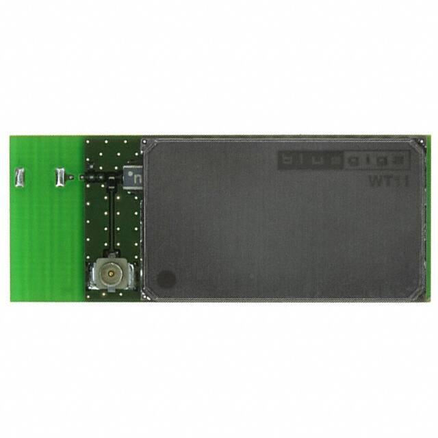


 工商网监
湘ICP备2023018690号
工商网监
湘ICP备2023018690号
