AYL1
For LED
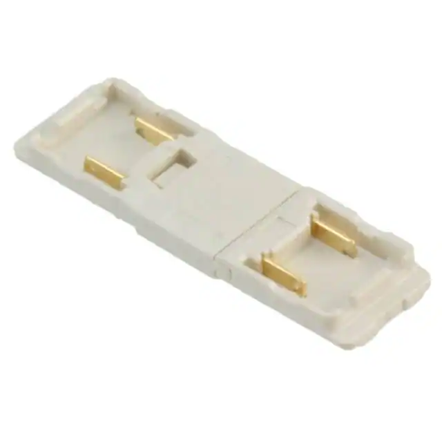
LED lighting connector
L1 Series
(Joint type)
FEATURES
New
1. Small and low profile design does
not obstruct the LED light
The connector is of a 2.4 mm pitch two
pins board joint type. The LED light is not
obstructed by the low profile (1.4 mm
mated height) L1 series connector.
Explanatory diagram of the connector
mounted on a circuit board
Joint plug
3. Safety covered by ensuring
insulation distance (Min. 1.6 mm)
4. Mating lock construction using
molded lock
5. Unmating configured with jig
APPLICATIONS
Straight LED tube lights, LED base
lights, etc.
Receptacle (common)
1.4mm
LED
RoHS compliant
4.4mm
LED mounted board
2. Floating design
The three-directional floating function
(X: ±0.3 mm, Y: ±0.5 mm, Z: ±0.3 mm)
accommodates thermal expansion of
circuit boards.
X-direction: ±0.3 mm
Y-direction: ±0.5 mm
Z-direction: ±0.3 mm
ORDERING INFORMATION
AYL 1
1
2
4
0
1: L1
Product type
1: Receptacle
2: Joint plug
Type of mating
1: Vertical
Number of pins (1 digit)
Terminal pitch
4: 2.4 mm
Function
0: Standard
ACCTB50E 201207-T
Panasonic Corporation
Automation Controls Business Unit
industrial.panasonic.com/ac/e/
�AYL1
PRODUCT TYPES
1. Receptacle
Mated height
Part No.
1.4mm
AYL111240
Mated height
Part No.
1.4mm
AYL121240
Packing
Inner carton (1-reel)
5,000 pieces
Outer carton
10,000 pieces
2. Joint plug
Packing
Inner carton (1-reel)
5,000 pieces
Outer carton
10,000 pieces
Notes: 1. Order unit:
For volume production: 1-inner carton (1-reel) units
Samples for mounting check: 50-connector units. Please contact our sales office.
2. Please contact us for connectors having a number of pins other than those listed above.
SPECIFICATIONS
1. Characteristics
Electrical
characteristics
Item
Rated current
Rated voltage
1.0A/pin contact
125V AC/DC
Breakdown voltage
1,250V AC for 1 min.
Insulation resistance
Min. 1,000MΩ (initial)
Contact resistance
Max. 90mΩ
Composite insertion force
(initial)
Composite removal force
(initial)
Specifications
Conditions
No short-circuiting or damage at a detection current of 1 mA
when the specified voltage is applied for one minute.
Using 500V DC megger (applied for 1 min.)
Based on the contact resistance measurement method
specified by JIS C 5402.
Two contacts of receptacle and a post of joint plug
Max. 25.2N
Insertion force of two receptacles and a joint plug
Min. 4.0N
Removal force of two receptacles and a joint plug
Y
Mechanical
characteristics
Floating distance
(Receptacle and joint plug
mated)
X direction: ±0.3 mm
Y direction: ±0.5 mm
Z direction: ±0.3 mm
X
Z
Ambient temperature
–40°C to +105°C
No freezing at low temperatures. No dew condensation.
Storage temperature
–40°C to +85°C (product only)
–40°C to +50°C (packing structure)
No freezing at low temperatures. No dew condensation.
Conformed to MIL-STD-202F, method 107G
Thermal shock resistance
(Receptacle and plug)
Order Temperature (°C)
1
–40 −30
2
3
105 +30
4
–40 −30
200 cycles,
insulation resistance min. 100MΩ,
contact resistance max. 90mΩ
Environmental
characteristics
Humidity resistance
(Receptacle and plug)
Saltwater spray resistance
(Receptacle and plug)
H2S resistance
(Receptacle and plug)
Durability
Soldering
temperature
resistance
Receptacle
Solder paste thickness
500 hours,
insulation resistance min. 100MΩ,
contact resistance max. 90mΩ
24 hours,
insulation resistance min. 100MΩ,
contact resistance max. 90mΩ
Time (minutes)
30
Max. 5
30
Max. 5
Bath temperature 85±2°C,
humidity 80 to 85% R.H.
Conformed to MIL-STD-1344F, method 1001
Bath temperature 35±2°C,
saltwater concentration 5±1%
Conformed to JEIDA-38-1984
Bath temperature 40±2°C, gas concentration 3±1 ppm,
humidity 75 to 80% R.H.
48 hours,
contact resistance max. 90mΩ
3 times,
contact resistance max. 90mΩ
Using removal tool
The initial specification must be satisfied electrically
and mechanically
Reflow soldering:
Max. peak temperature of 260°C, Max. 2 times
(PC board surface temperature near connector terminals)
Soldering iron: 300°C within 5 s
350°C within 3s
The initial specification must be satisfied electrically
and mechanically
Recommendation t = 0.12 mm screen
Note: The preceding show characteristics, when mated with receptacle and Joint plug.
Panasonic Corporation
Automation Controls Business Unit
industrial.panasonic.com/ac/e/
ACCTB50E 201207-T
�AYL1
2. Material and surface treatment
1. Receptacle
Part name
Molded portion
Material
LCP resin (UL94V-0)
Color
White
Contact
Copper alloy
—
Soldering terminal
Copper alloy
—
Material
LCP resin (UL94V-0)
Copper alloy
Color
White
—
Surface treatment
—
Contact portion: Pd-Ni+Au flash plating over Ni
Terminal portion: Au plating over Ni (except the terminal tips)
Terminal portion: Au plating over Ni
2. Joint plug
Part name
Molded portion
Post
Surface treatment
—
Terminal portion: Pd-Ni+Au flash plating over Ni
DIMENSIONS (Unit: mm)
Receptacle
Terminal coplanarity
0.08
0.20±0.03
2.42
X
X
(Contact and
soldering terminals)
3.78
Y
2.00
(Suction face)
2.40±0.05
3.02
Y
0.90±0.05
0.38
0.60
General tolerance: ±0.2
1.00
0.19
0.15
0.75
4.40
15.00
2.40±0.05
1.60 (Suction face)
Joint plug
1.38
13.62
1.35
1.15
3.22
3.00
3.08
9.60
General tolerance: ±0.2
ACCTB50E 201207-T
Panasonic Corporation
Automation Controls Business Unit
industrial.panasonic.com/ac/e/
�AYL1
Receptacle and Joint plug are mated
Joint plug
Receptacle
1.40±0.1
Receptacle
EMBOSSED TAPE DIMENSIONS (Unit: mm)
(1.75)
(17.4±1)
Top cover tape
Label
Top cover tape
Embossed carrier tape
Embossed carrier tape
to 18
0°
380 dia.
Note 1)
(4.0)
(16.0 +0.3
−0.1 )
(7.5)
• Specifications for the plastic reel
(In accordance with EIAJ ET-7200B.)
(8.0) (2.0)
1.
5
Embossed mounting-hole
165°
Leading direction after packaging
• Tape packed status
Receptacle
Taping reel
Receptacle
+0
0 .1
dia
.
(24.0 +0.3
−0.1 )
(11.50)
Top cover tape
(1.75)
(25.4±1)
Label
0°
to 18
5
165°
1.
+0
0 .1
Top cover tape
Embossed carrier tape
Embossed carrier tape
380 dia.
Note 1)
(4.0)
(8.0) (2.0)
Leading direction after packaging
Joint plug
Embossed mounting-hole
Joint plug
Taping reel
dia
.
• Connector orientation with respect to embossed tape feeding direction
Type
L1
Direction
of tape progress
Receptacle
Panasonic Corporation
Automation Controls Business Unit
Joint plug
industrial.panasonic.com/ac/e/
ACCTB50E 201207-T
�AYL1
NOTES ON USING CONNECTOR FOR LED LIGHTING
Recommended PC board pattern (mounting pad layout)
(TOP VIEW)
Unit: mm
0.05±0.03
2.32±0.03
0.05±0.03
Note 3) Between
ACCTB50E 201207-T
Panasonic Corporation
2.40±0.03
0.40±0.03
PC board: Max. 1.00
Note 1)
1.10±0.03
Note 2)
0.20±0.05
Note 2)
Note 2) 0.20±0.05
0.20±0.05
Note 2) 0.20±0.05
Note 1)
Pad area
Note 2)
It is necessary to do the resist processing on the copper foil.
Note 3) These dimensions are applied when the insulation distance from the edge of the PC board is 1.5 mm.
2) Reflow soldering
• Screen-printing is recommended for printing paste solder.
• To determine the relationship between the screen opening area
and the PC board foot pattern area, refer to the diagrams in the
recommended patterns for PC boards and metal masks.
Make sure to use the terminal tip as a reference position when
setting.
• Too much solder may cause solder creeping near the
contacting part or contact failure.
Terminal
� About receptacle
• PC board design
Design the recommended foot pattern in order to secure the
mechanical strength in the soldered areas of the terminal.
• Connector mounting
When mounting, if there is too much suction nozzle pressure,
the molded and metal parts might deform and break.
Please check beforehand.
In case of dry condition, please care the occurrence of static
electricity.
The product may be adhered to the embossed carrier tape or
the cover tape in dry condition.
Recommended humidity is between 40 to 60 % and please
remove static electricity by ionizer in manufacturing scene.
• Soldering
1) Manual soldering.
• Since this connector is the low profile type the amount of solder
supplied should be closely monitored.
Too much solder during manual soldering may cause solder
creeping near the contacting part or contact failure.
• Make sure that the soldering iron tip is heated within the
temperature and time limits indicated in the specifications.
• Flux from the solder wire may adhere to the contact surfaces
during soldering operations. After soldering, carefully check the
contact surfaces with a magnifying glass and clean off any flux
before use.
• Be aware that a load applied to the connector terminals while
soldering may displace the contact.
• Thoroughly clean the soldering iron tip.
Note 1) 1.10±0.03
11.92±0.05
0.40±0.03
Note 3) (Min. 1.84)
� Safety precautions
Observe the following safety precautions to prevent accidents
and injuries.
1) The use of the connector outside of the specified rated current
and breakdown voltage ranges may cause abnormal heating,
smoke, and fire.
Never use the connector beyond the specified ranges of the
product.
2) In order to avoid accidents, make sure you have thoroughly
reviewed the specifications before use.
Consult us if you plan to use the product in a way not covered by
the specifications.
3) We are consistently striving to improve quality and reliability.
However, the fact remains that electrical components and
devices generally fail at a given statistical probability.
Furthermore, their durability varies depending on where and
how they are used. Please be sure to verify electrical
components and devices under actual conditions before use.
Continuously using them in a state of degraded performance
may cause deterioration in insulation performance, thus
resulting in abnormal heat generation, smoke generation, or fire.
To avoid that, we ask you to implement safe designs that include
redundancy, fire prevention, and malfunction prevention. Also,
please conduct periodic maintenance so that no accidents
resulting in injury or death, fire, or harm to society will be caused
as a result of product failure or service life.
Paste
solder
PC board
foot pattern
• Consult us when using a screen-printing thickness other than
that recommended.
• Depending on the size of the connector being used, self
alignment may not be possible. Accordingly, carefully position
the terminal with the PC board pattern.
• The recommended reflow temperature profile is given in the
figure below
Upper limit (Soldering heat resistance)
Lower limit (Solder wettability)
Temperature
260°C
230°C
180°C
150°C
Peak temperature
Preheating
220°C
200°C
25 sec.
60 to 120 sec.
70 sec.
Time
• The temperature is measured on the surface of the PC board
near the connector terminal.
• Certain solder and flux types may cause serious solder
creeping.
Solder and flux characteristics should be taken into
consideration when setting the reflow soldering conditions.
• Do not apply adhesive to secure the connector, because it can
affect the spring action of the contact.
• When coating the PC board after soldering the connector to
prevent the deterioration of insulation, perform the coating in
such a way so that the coating does not get on the connector.
3) Reworking on a soldered portion
• Finish reworking in one operation.
• For reworking of the solder bridge, use a soldering iron with a
flat tip. Do not add flux, otherwise, the flux may creep to the
contact parts.
• Use a soldering iron whose tip temperature is within the
temperature range specified in the specifications.
Automation Controls Business Unit
industrial.panasonic.com/ac/e/
�AYL1
• Although this product has floating structure, it’s the
performance in the state of receptacles and a plug mated. We
can’t guarantee mating in the state where receptacles and a
plug are shifted from the center. When inserting a plug in
receptacles, please check the position of a mutual receptacle.
Position
sifts
Joint plug
Joint plug
Position
sifts
Receptacle
Position
sifts
• Do not drop or handle the connector carelessly. Otherwise, the
terminals may become deformed due to excessive force or
applied solderability may degrade.
• When cutting or bending the PC board after mounting the
connector, be careful that the soldered sections are subjected to
excessive forces.
� Insertion / Removal and mating retention of connectors
• Do not insert or remove the connector when it is not soldered.
Also, forcibly applied external pressure on the terminals can
weaken the adherence of the terminals to the molded part or
cause the terminals to lose their evenness.
• Excessive prying-force applied to one end may cause product
breakage and separation of the solder joints at the terminal.
Excessive force applied for insertion in a pivot action as shown
may also cause product breakage.
Always align the connector with the mating part and slide it in
parallel.
Mating
X
Z
Receptacle
X
Y
Receptacle
Joint plug
Joint plug
Z
Z
Y
Y
Receptacle
Receptacle
• Pushing the plug excessively when inserting it may deform and
break the product.
• This product has simple lock structure for mating. However,
connectors may be unmated because of impact by dropping and
so on. Please take countermeasures at the equipment side for
preventing removal of connectors. In order to prevent removal of
connectors, please fix the PC board by frame and so on not to
move more than floating distance, especially the neighborhood
of connectors.
Receptacle
Fix the PC board by frame and so on
Z
Y
PC board with mounted connectors
(Don’t move more than floating distance)
• When removing the connector, please use the recommended
removal tool.
After inserting the tip of removal jig under the plug, push down
the jig shown in below. (Removable from either the left or right
side) Since holding force of mating will decline when removing
the connector without using tool, please don’t use the remove
plug, and exchange to a new plug.
Removal tool
Z
Insert removal tool and push down
in the direction of the arrow.
Y
X
Z
Insertion point
of removal tool
Panasonic Corporation
Y
Automation Controls Business Unit
industrial.panasonic.com/ac/e/
ACCTB50E 201207-T
�


 工商网监
湘ICP备2023018690号
工商网监
湘ICP备2023018690号
