DME50C01
Silicon PNP epitaxial planar type (Tr1)
Silicon NPN epitaxial planar type (Tr2)
Unit: mm
For general amplification
DME20C01 in SMini5 type package
Features
High forward current transfer ratio hFE with excellent linearity
Low collector-emitter saturation voltage VCE(sat)
Halogen-free / RoHS compliant
(EU RoHS / UL-94 V-0 / MSL: Level 1 compliant)
Marking Symbol: A4
Basic Part Number
DSA2001 + DSC2001 (Base-emitterr connection)
Packaging
DME50C010R Embossed type (Thermo-compression sealing): 3 000 pcs / reel (standard)
Absolute Maximum Ratings Ta = 25°C
Parameter
Tr1
Tr2
Overall
Symbol
Rating
Unit
Collector-base voltage (Emitter open)
VCBO
–60
V
Collector-emitter voltage (Base open)
VCEO
–50
V
Emitter-base voltage (Collector open)
VEBO
–7
V
Collector current
IC
–100
mA
Peak collector current
ICP
–200
mA
Collector-base voltage (Emitter open)
VCBO
60
V
Collector-emitter voltage (Base open)
VCEO
50
V
Emitter-base voltage (Collector open)
VEBO
7
V
Collector current
IC
100
mA
Peak collector current
ICP
200
mA
Total power dissipation
PT
150
mW
Junction temperature
Tj
150
°C
Operating ambient temperature
Topr
–40 to +85
°C
Storage temperature
Tstg
–55 to +150
°C
Publication date: January 2014
Ver. CED
1: Emitter (Tr1)
2: Base (Tr1)
Emitter (Tr2)
Panasonic
JEITA
Code
(C1)
5
Tr1
3: Base (Tr2)
4: Collector (Tr2)
5: Collector (Tr1)
SMini5-F3-B
SC-113CB
SOT-353
(C2)
4
Tr2
1
2
3
(E1) (B1,E2) (B2)
1
�DME50C01
Electrical Characteristics Ta = 25°C±3°C
Tr1
Parameter
Symbol
Conditions
Min
Typ
Max
Unit
Collector-base voltage (Emitter open)
VCBO
IC = –10 µA, IE = 0
–60
V
Collector-emitter voltage (Base open)
VCEO
IC = –2 mA, IB = 0
–50
V
Emitter-base voltage (Collector open)
VEBO
IE = –10 µA, IC = 0
–7
V
Collector-base cutoff current (Emitter open)
ICBO
VCB = –20 V, IE = 0
– 0.1
µA
Collector-emitter cutoff current (Base open)
ICEO
VCE = –10 V, IB = 0
–100
µA
Forward current transfer ratio
hFE
VCE = –10 V, IC = –2 mA
460
– 0.5
V
Collector-emitter saturation voltage
VCE(sat)
Transition frequency
fT
Collector output capacitance
(Common base, input open circuited)
Cob
210
IC = –100 mA, IB = –10 mA
– 0.2
VCE = –10 V, IC = –2 mA
150
MHz
2
pF
VCB = –10 V, IE = 0, f = 1 MHz
Note) Measuring methods are based on JAPANESE INDUSTRIAL STANDARD JIS C 7030 measuring methods for transistors.
Tr2
Parameter
Symbol
Conditions
Min
Typ
Max
Unit
Collector-base voltage (Emitter open)
VCBO
IC = 10 µA, IE = 0
60
V
Collector-emitter voltage (Base open)
VCEO
IC = 2 mA, IB = 0
50
V
Emitter-base voltage (Collector open)
VEBO
IE = 10 µA, IC = 0
7
V
Collector-base cutoff current (Emitter open)
ICBO
VCB = 20 V, IE = 0
0.1
µA
Collector-emitter cutoff current (Base open)
ICEO
VCE = 10 V, IB = 0
100
µA
Forward current transfer ratio
hFE
VCE = 10 V, IC = 2 mA
460
0.3
V
Collector-emitter saturation voltage
VCE(sat)
Transition frequency
fT
Collector output capacitance
(Common base, input open circuited)
Cob
210
IC = 100 mA, IB = 10 mA
0.13
VCE = 10 V, IC = 2 mA
150
MHz
VCB = 10 V, IE = 0, f = 1 MHz
1.5
pF
Note) Measuring methods are based on JAPANESE INDUSTRIAL STANDARD JIS C 7030 measuring methods for transistors.
Common characteristics chart
DME50C01_PT-Ta
PT Ta
Total power dissipation PT (mW)
200
150
100
50
0
0
40
80
120
160
200
Ambient temperature Ta (°C)
Ver. CED
2
�DME50C01
Characteristics
charts of Tr1
DME50C01(Tr1)_IC-VCE
DME50C01(Tr1)_hFE-IC
−120
−80
−400 µA
−300 µA
−60
−200 µA
−40
−100 µA
−20
−2
−4
−6
−8
−10
500
400
Ta = 85°C
300
25°C
200
100
0
− 0.1
−12
Collector-emitter voltage VCE (V)
Collector current IC (mA)
−80
−40°C
−60
−40
−20
− 0.4
− 0.8
−1.2
Collector output capacitance
(Common base, input open circuited) Cob (pF)
25°C
Ta = 85°C
0
−10
2.0
1.0
0
−1
−10
150 µA
100 µA
50 µA
4
6
8
10
12
Collector-emitter voltage VCE (V)
Forward current transfer ratio hFE
Collector current IC (mA)
200 µA
2
50
Ta = 85°C
25°C
300
−40°C
200
100
0
0.1
1
10
Collector current IC (mA)
Ver. CED
−10
−100
VCE(sat) IC
500
400
−1
Collector current IC (mA)
DME50C01(Tr2)_VCEsat-IC
VCE = 10 V
IB = 250 µA
0
100
0
− 0.1
−100
600
20
150
hFE IC
100
−100
VCE = −10 V
Ta = 25°C
200
DME50C01(Tr2)_hFE-IC
Ta = 25°C
−10
250
Collector-base voltage VCB (V)
120
40
−1
DME50C01(Tr1)_fT-IC
3.0
IC VCE
60
− 0.01
− 0.1
Collector current IC (mA)
IE = 0
f = 1 MHz
Ta = 25°C
Characteristics
charts of Tr2
DME50C01(Tr2)_IC-VCE
0
−100
−40°C
fT IC
4.0
Base-emitter voltage VBE (V)
80
Ta = 85°C
25°C
Cob VCB
−120
0
−1
DME50C01(Tr1)_Cob-VCB
IC VBE
−100
IC / IB = 10
Collector current IC (mA)
DME50C01(Tr1)_IC-VBE
VCE = −10 V
−1
−10
− 0.1
−40°C
Transition frequency fT (MHz)
0
VCE = −10 V
100
Collector-emitter saturation voltage VCE(sat) (V)
Collector current IC (mA)
−500 µA
Forward current transfer ratio hFE
IB = −600 µA
−100
0
VCE(sat) IC
600
Ta = 25°C
DME50C01(Tr1)_VCEsat-IC
hFE IC
Collector-emitter saturation voltage VCE(sat) (V)
IC VCE
10
IC / IB = 10
1
0.1
0.01
0.1
Ta = 85°C
−40°C
25°C
1
10
100
Collector current IC (mA)
3
�DME50C01
DME50C01(Tr2)_IC-VBE
Collector current IC (mA)
100
Ta = 85°C
80
−40°C
60
40
20
0
0
0.2
0.4
0.6
0.8
1.0
Base-emitter voltage VBE (V)
1.2
fT IC
250
VCE = 10 V
Ta = 25°C
4.0
Transition frequency fT (MHz)
25°C
Collector output capacitance
(Common base, input open circuited) Cob (pF)
Cob VCB
120
VCE = 10 V
DME50C01(Tr2)_fT-IC
DME50C01(Tr2)_Cob-VCB
IC VBE
3.0
2.0
1.0
0
1
10
100
Collector-base voltage VCB (V)
Ver. CED
200
150
100
50
0
0.1
1
10
100
Collector current IC (mA)
4
�DME50C01
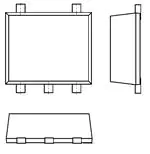
SMini5-F3-B
Unit: mm
Land Pattern (Reference) (Unit: mm)
Ver. CED
5
�Request for your special attention and precautions
in using the technical information and semiconductors described in this book
(1) If any of the products or technical information described in this book is to be exported or provided to non-residents, the
laws and regulations of the exporting country, especially, those with regard to security export control, must be observed.
(2) The technical information described in this book is intended only to show the main characteristics and application circuit
examples of the products. No license is granted in and to any intellectual property right or other right owned by
Panasonic Corporation or any other company. Therefore, no responsibility is assumed by our company as to the
infringement upon any such right owned by any other company which may arise as a result of the use of technical
information de-scribed in this book.
(3) The products described in this book are intended to be used for general applications (such as office equipment,
communications equipment, measuring instruments and household appliances), or for specific applications as expressly
stated in this book.
Please consult with our sales staff in advance for information on the following applications, moreover please exchange
documents separately on terms of use etc.: Special applications (such as for in-vehicle equipment, airplanes, aerospace,
automotive equipment, traffic signaling equipment, combustion equipment, medical equipment and safety devices) in
which exceptional quality and reliability are required, or if the failure or malfunction of the products may directly
jeopardize life or harm the human body.
Unless exchanging documents on terms of use etc. in advance, it is to be understood that our company shall not be held
responsible for any damage incurred as a result of or in connection with your using the products described in this book
for any special application.
(4) The products and product specifications described in this book are subject to change without notice for modification
and/or improvement. At the final stage of your design, purchasing, or use of the products, therefore, ask for the most upto-date Product Standards in advance to make sure that the latest specifications satisfy your requirements.
(5) When designing your equipment, comply with the range of absolute maximum rating and the guaranteed operating
conditions (operating power supply voltage and operating environment etc.). Especially, please be careful not to exceed
the range of absolute maximum rating on the transient state, such as power-on, power-off and mode-switching. Otherwise, we will not be liable for any defect which may arise later in your equipment.
Even when the products are used within the guaranteed values, take into the consideration of incidence of break down
and failure mode, possible to occur to semiconductor products. Measures on the systems such as redundant design,
arresting the spread of fire or preventing glitch are recommended in order to prevent physical injury, fire, social damages,
for example, by using the products.
(6) Comply with the instructions for use in order to prevent breakdown and characteristics change due to external factors
(ESD, EOS, thermal stress and mechanical stress) at the time of handling, mounting or at customer's process. We do
not guarantee quality for disassembled products or the product re-mounted after removing from the mounting board.
When using products for which damp-proof packing is required, satisfy the conditions, such as shelf life and the elapsed
time since first opening the packages.
(7) When reselling products described in this book to other companies without our permission and receiving any claim of
request from the resale destination, please understand that customers will bear the burden.
(8) This book may be not reprinted or reproduced whether wholly or partially, without the prior written permission of our
company.
No.010618
�


 工商网监
湘ICP备2023018690号
工商网监
湘ICP备2023018690号
