2018
CATALOG
EMC Components
ESD Components
2018.3
industrial.panasonic.com/
�EMC Components / ESD Components CONTENTS
Classification
Product Item
Part No.
Page
Safety Precautions (Common precautions for EMC Components and ESD Suppressor)
Common mode Noise Filters
EMC Components
Common mode Noise Filter Array
2
EXC X4CZ
3
EXC X4CH
5
EXC X4CE
7
EXC X4CT
9
EXC 14CH
11
EXC 14CG, 14CE
13
EXC 14CT
16
EXC 14CX
18
EXC 16CT
20
EXC 24CH
22
EXC 24CG
24
EXC 24CE, 24CF
26
EXC 34CG, 34CE
28
EXC 18CG, 18CE
30
EXC 28CH
32
EXC 28CG
34
EXC 28CE
36
Common specifications for Common mode Noise Filters / Array
Common mode Noise Filters with ESD Suppressor
Common mode Noise Filter Array with ESD Suppressor
38
EXC 14CS
40
EXC 24CS
42
EXC 18CS
44
Common specifications for Common mode Noise Filters with ESD Suppressor
46
EXC 14CP
48
EXC 24CB, 24CP, 24CN
50
ELK EA, E, EV
54
EZA EG2A, EG3A
60
EZA EG1N, EG2N
62
ESD Suppressor Array
EZA EGCA
64
ESD Suppressor High Withstanding Type
EZA EG3W
66
2 mode Noise Filters
Coil type EMI Filters
ESD Suppressor
Common specifi cations for ESD Suppressor / Array
ESD Components
68
Multilayer Varistor (Automotive Grade)
EZJ Z-M / EZJ P-M
69
Multilayer Varistor
(DC voltage lines / High speed signal lines)
EZJ Z / EZJ P
80
Multilayer Varistor
(2 Array Type for high speed signal lines)
EZJ ZSV-A
85
Multilayer Varistor (DC voltage lines)
EZJZ S
87
Common specifi cations for Multilayer Varistor
89
All products in this catalog comply with the RoHS Directive.
The RoHS Directive is “the Directive (2011/65/EU) on the Restriction of the Use of Certain
Hazardous Substances in Electrical and Electronic Equipment “ and its revisions.
04
–1–
Mar. 2018
�Safety Precautions (Common precautions for EMC Components and ESD Suppressor)
• When using our products, no matter what sort of equipment they might be used for, be sure to make a written
agreement on the specifications with us in advance. The design and specifications in this catalog are subject
to change without prior notice.
• Do not use the products beyond the specifications described in this catalog.
• This catalog explains the quality and performance of the products as individual components. Before use, check
and evaluate their operations when installed in your products.
• Install the following systems for a failsafe design to ensure safety if these products are to be used in equipment
where a defect in these products may cause the loss of human life or other significant damage, such as damage to
vehicles (automobile, train, vessel), traffic lights, medical equipment, aerospace equipment, electric heating
appliances, combustion/gas equipment, rotating equipment, and disaster/crime prevention equipment.
✽ Systems equipped with a protection circuit and a protection device
✽ Systems equipped with a redundant circuit or other system to prevent an unsafe status in the event of a single fault
(1) Precautions for use
• These products are designed and manufactured for general and standard use in general electronic equipment
(e.g. AV equipment, home electric appliances, office equipment, information and communication equipment)
• These products are not intended for use in the following special conditions. Before using the products,
carefully check the effects on their quality and performance, and determine whether or not they can be used.
1. In liquid, such as water, oil, chemicals, or organic solvent
2. In direct sunlight, outdoors, or in dust
3. In salty air or air with a high concentration of corrosive gas, such as Cl2, H2S, NH3, SO2, or NO2
4. Electric Static Discharge (ESD) Environment (except ESD Suppressors)
These components are sensitive to static electricity and can be damaged under static shock (ESD).
Please take measures to avoid any of these environments.
Smaller components are more sensitive to ESD environment.
5. Electromagnetic Environment
Avoid any environment where strong electromagnetic waves exist.
6. In an environment where these products cause dew condensation
7. Sealing or coating of these products or a printed circuit board on which these products are mounted, with
resin or other materials
• These products generate Joule heat when energized. Carefully position these products so that their heat will
not affect the other components.
• Carefully position these products so that their temperatures will not exceed the category temperature range due
to the effects of neighboring heat-generating components. Do not mount or place heat-generating components
or inflammables, such as vinyl-coated wires, near these products.
• Note that non-cleaning solder, halogen-based highly active flux, or water-soluble flux may deteriorate the
performance or reliability of the products.
• Carefully select a flux cleaning agent for use after soldering. An unsuitable agent may deteriorate the performance
or reliability. In particular, when using water or a water-soluble cleaning agent, be careful not to leave water
residues. Otherwise, the insulation performance may be deteriorated.
(2) Precautions for storage
• Do not store these products in the following conditions. Otherwise, their electrical performance and/or
solderability may be deteriorated, and the packaging materials (e.g. taping materials) may be deformed or
deteriorated, resulting in mounting failures.
1. In salty air or in air with a high concentration of corrosive gas, such as Cl2, H2S, NH3, SO2, or NO2
2. In direct sunlight
Package markings include the product number, quantity, and country of origin.
In principle, the country of origin should be indicated in English.
01 Dec. 2016
–2–
�Common mode Noise Filters
Common mode Noise Filters
EXCX4CZ
Type:
Features
● Small
and thin (L 0.65 mm×W 0.50 mm×H 0.30 mm)
mode attenuation at 2.4GHz, Suitable for noise suppression at Wi-Fi band
● Strong multilayer/sintered structure, excellent reflow resistance and high mounting reliability
● Lead, halogen and antimony-free
● RoHS compliant
● High-common
Recommended Applications
● Smartphones,
● Suppresses
Tablet PCs and DSC
noise radiation to Wi-Fi Equipment
Explanation of Part Numbers
1
2
3
4
5
6
7
8
9
10
11
E
X
C
X
4
C
Z
2
0
0
X
Size
Number of
Terminals
Product Code
Noise Filter
Code Dimensions(mm)
X
4 Terminals C
Type Characteristics
Coupled
type
Z
Nominal Impedance
Wide band width,
high attenuation
0.65 × 0.50 × 0.30
(L) × (W) × (H)
Construction
12
Form
Suffix
The first two digits are
Code
Packing
significant figure of
Pressed Carrier Taping
impedance value, and the
X
2 mm pitch, 10,000 pcs.
third one denotes the
number of zeros following
Dimensions in mm (not to scale)
F
Ceramics
D
C
E
A
B
Part No.
(inch size)
Electrode
Inner Conductor
Dimensions (mm)
A
B
C
D
E
F
EXCX4CZ 0.50±0.05 0.65±0.05 0.30±0.05 0.12±0.10 0.40±0.10 0.15±0.10
(0202)
Mass
(Weight)
[mg/pc.]
0.28
Circuit Configuration (No Polarity)
4
3
4
3
●
1
2
1
2
The pin numbers shown here are for reference purposes
only. Confirm the actual pin number arrangement with
the exchanged specification documents.
Design and specifications are each subject to change without notice. Ask factory for the current technical specifications before purchase and/or use.
Should a safety concern arise regarding this product, please be sure to contact us immediately.
03
–3–
Oct. 2015
�Common mode Noise Filters
Ratings
Part Number
Impedance (Ω) at 100 MHz
Common Mode
Rated Voltage
(V DC)
Rated Current
(mA DC)
DC Resistance
(Ω)max.
20 Ω±30 %
10
100
3.0±30 %
EXCX4CZ200X
●
Category Temperature Range –40 °C to +85 °C
Impedance Characteristics (Typical)
●
EXCX4CZ200X
Impedance (Ω)
10000
1000
Common Mode
100
10
Differential Mode
1
●
1
10
100
Frequency (MHz)
1000
10000
Measurement Circuit
(A) Common Mode
(B) Differential Mode
Z
Z
Attenuation Characteristics (Typical)
●
EXCX4CZ200X
Attenuation (dB)
0
-5
Differential Mode
-10
-15
-20
-25
-30
-35
-40
-45
-50
Common Mode
100
1000
Frequency (MHz)
10000
■ As for Packaging Methods, Land Pattern, Soldering Conditions and Safety Precautions,
Please see Data Files
Design and specifications are each subject to change without notice. Ask factory for the current technical specifications before purchase and/or use.
Should a safety concern arise regarding this product, please be sure to contact us immediately.
03
–4–
Oct. 2015
�Common mode Noise Filters
Common mode Noise Filters
EXCX4CH
Type:
Features
● Small
and thin (L 0.65 mm×W 0.50 mm×H 0.30 mm)
common mode attenuation in high-speed differential transmission lines, Cut-off frequency is more than
8.5 GHz, and an influence to differential transmission signal quality is little
● Strong multilayer/sintered structure, excellent reflow resistance and high mounting reliability
● Lead, halogen and antimony-free
● RoHS compliant
● High
Recommended Applications
● Smartphones,
● Noise
Tablet PCs and DSC
suppression of high-speed differential data lines such as USB, LVDS and HDMI
Explanation of Part Numbers
1
2
3
4
5
6
7
8
9
10
11
E
X
C
X
4
C
H
3
5
0
X
Size
Number of
Terminals
Product Code
Noise Filter
Code Dimensions(mm)
X
4 Terminals C
Type Characteristics
Coupled
type
0.65 × 0.50 × 0.30
(L) × (W) × (H)
H
Nominal Impedance
12
Form
Suffix
The first two digits are
High speed
Code
Packing
Differential transmission significant figure of
Pressed
Carrier Taping
impedance value, and the
X
2 mm pitch, 10,000 pcs.
third one denotes the
number of zeros following
Construction
Dimensions in mm (not to scale)
F
E
Ceramics
Ferrite
D
C
A
B
Inner Conductor
Electrode
Part No.
(inch size)
Dimensions (mm)
A
B
C
D
E
F
EXCX4CH 0.50±0.05 0.65±0.05 0.30±0.05 0.12±0.10 0.40±0.10 0.15±0.10
(0202)
Mass
(Weight)
[mg/pc.]
0.43
Circuit Configuration (No Polarity)
4
3
4
3
●
1
2
1
2
The pin numbers shown here are for reference purposes
only. Confirm the actual pin number arrangement with
the exchanged specification documents.
Design and specifications are each subject to change without notice. Ask factory for the current technical specifications before purchase and/or use.
Should a safety concern arise regarding this product, please be sure to contact us immediately.
00 Feb. 2016
–5–
�Common mode Noise Filters
Ratings
Impedance (Ω) at 100 MHz
Common Mode
Rated Voltage
(V DC)
Rated Current
(mA DC)
DC Resistance
(Ω)max.
EXCX4CH120X
12 Ω±5 Ω
5
100
2.0
EXCX4CH350X
35 Ω±30 %
5
100
2.7
Part Number
●
Category Temperature Range –40 °C to +85 °C
Impedance Characteristics (Typical)
●
●
EXCX4CH120X
EXCX4CH350X
1000
100
Impedance (Ω)
Impedance (Ω)
1000
Common Mode
10
Common Mode
100
10
Differential Mode
Differential Mode
1
●
1
10
100
Frequency (MHz)
1000
1
10000
1
10
1000
10000
Measurement Circuit
(A) Common Mode
(B) Differential Mode
Z
Z
Insertion Loss (Typical)
Common mode Attenuation Characteristics (Typical)
0
0
Attenuations (dB)
Attenuations (dB)
100
Frequency (MHz)
EXCX4CH350
-5
EXCX4CH120
-10
-15
-5
-10
EXCX4CH350
-15
EXCX4CH120
-20
-25
-20
1
10
100
Frequency (MHz)
1000
-30
10000
1
10
100
Frequency (MHz)
1000
10000
■ As for Packaging Methods, Land Pattern, Soldering Conditions and Safety Precautions,
Please see Data Files
Design and specifications are each subject to change without notice. Ask factory for the current technical specifications before purchase and/or use.
Should a safety concern arise regarding this product, please be sure to contact us immediately.
00 Feb. 2016
–6–
�Common mode Noise Filters
Common mode Noise Filters
EXCX4CE
Type:
Features
● Small
and thin (L 0.65 mm×W 0.50 mm×H 0.30 mm)
suppression of high-speed differential transmission lines with little influence of waveform rounding on
signal transmission
● Strong multilayer/sintered structure, excellent reflow resistance and high mounting reliability
● Lead, halogen and antimony-free
● RoHS compliant
● Noise
Recommended Applications
● Smartphones,
● Noise
Tablet PCs and DSC
suppression of high-speed differential data lines such as MIPI, USB and LVDS
Explanation of Part Numbers
1
2
3
4
5
6
7
8
9
10
11
E
X
C
X
4
C
E
9
0
0
U
Size
Number of
Terminals
Product Code
Noise Filter
Code Dimensions(mm)
X
4 Terminals C
Type Characteristics
Coupled
type
E
Nominal Impedance
High speed
Differential transmission
0.65 × 0.50 × 0.30
(L) × (W) × (H)
Construction
12
Form
Suffix
The first two digits are
Code
Packing
significant figure of
Pressed Carrier Taping
impedance value, and the
U
2 mm pitch, 10,000 pcs.
third one denotes the
number of zeros following
Dimensions in mm (not to scale)
F
Ferrite
D
C
E
A
B
Part No.
(inch size)
Electrode
Inner Conductor
Dimensions (mm)
A
B
C
D
E
F
EXCX4CE 0.50±0.05 0.65±0.05 0.30±0.05 0.12±0.10 0.40±0.10 0.15±0.10
(0202)
Mass
(Weight)
[mg/pc.]
0.56
Circuit Configuration (No Polarity)
4
3
4
3
●
1
2
1
2
The pin numbers shown here are for reference purposes
only. Confirm the actual pin number arrangement with
the exchanged specification documents.
Design and specifications are each subject to change without notice. Ask factory for the current technical specifications before purchase and/or use.
Should a safety concern arise regarding this product, please be sure to contact us immediately.
03
–7–
Oct. 2015
�Common mode Noise Filters
Ratings
Impedance (Ω) at 100 MHz
Common Mode
Differential Mode
Rated Voltage
(V DC)
Rated Current
(mA DC)
DC Resistance
(Ω)max.
EXCX4CE600U
60 Ω±20 %
18 Ω max.
5
100
2.4±30 %
EXCX4CE900U
90 Ω±20 %
20 Ω max.
5
100
3.0±30 %
Part Number
●
Category Temperature Range –40 °C to +85 °C
Impedance Characteristics (Typical)
●
●
EXCX4CE600U
EXCX4CE900U
1000
Impedance (Ω)
Impedance (Ω)
1000
Common Mode
100
10
Common Mode
100
10
Differential Mode
Differential Mode
1
●
1
10
100
Frequency (MHz)
1000
1
10000
1
10
100
Frequency (MHz)
1000
10000
Measurement Circuit
(A) Common Mode
(B) Differential Mode
Z
Z
■ As for Packaging Methods, Land Pattern, Soldering Conditions and Safety Precautions,
Please see Data Files
Design and specifications are each subject to change without notice. Ask factory for the current technical specifications before purchase and/or use.
Should a safety concern arise regarding this product, please be sure to contact us immediately.
03
–8–
Oct. 2015
�Common mode Noise Filters
Common mode Noise Filters
EXCX4CT
Type:
Features
● Small
and thin (L 0.65 mm×W 0.50 mm×H 0.30 mm)
● High attenuation at common-mode for noise suppression of harmonic signal components and cellular frequency
● Cut-off
frequency is more than 3 GHz, the insertion loss is low in differential transmission line
multilayer/sintered structure, excellent reflow resistance and high mounting reliability
● Lead, halogen and antimony-free
● RoHS compliant
● Strong
Recommended Applications
● Smartphones,
● Noise
Tablet PCs and DSC
suppression of high-speed differential data lines such as MIPI, USB and LVDS
Explanation of Part Numbers
1
2
3
4
5
6
7
8
9
10
11
E
X
C
X
4
C
T
9
0
0
X
Size
Number of
Terminals
Product Code
Noise Filter
Code Dimensions(mm)
X
4 Terminals C
Type Characteristics
Coupled
type
Nominal Impedance
T High attenuation type
0.65 × 0.50 × 0.30
(L) × (W) × (H)
Construction
12
Form
Suffix
The first two digits are
Code
Packing
significant figure of
Pressed Carrier Taping
impedance value, and the
X
2 mm pitch, 10,000 pcs.
third one denotes the
number of zeros following
Dimensions in mm (not to scale)
F
E
Ceramics
Ferrite
D
C
A
B
Inner Conductor
Part No.
(inch size)
Electrode
Dimensions (mm)
A
B
C
D
E
F
EXCX4CT 0.50±0.05 0.65±0.05 0.30±0.05 0.12±0.10 0.40±0.10 0.15±0.10
(0202)
Mass
(Weight)
[mg/pc.]
0.43
Circuit Configuration (No Polarity)
4
3
4
3
●
1
2
1
2
The pin numbers shown here are for reference purposes
only. Confirm the actual pin number arrangement with
the exchanged specification documents.
Design and specifications are each subject to change without notice. Ask factory for the current technical specifications before purchase and/or use.
Should a safety concern arise regarding this product, please be sure to contact us immediately.
00 Sep. 2015
–9–
�Common mode Noise Filters
Ratings
Impedance (Ω) at 100 MHz
Common Mode
Rated Voltage
(V DC)
Rated Current
(mA DC)
DC Resistance
(Ω)
EXCX4CT650X
65 Ω±20 %
10
100
2.7 Ω±30 %
EXCX4CT900X
90 Ω±20 %
10
100
3.0 Ω±30 %
Part Number
●
Category Temperature Range –40 °C to +85 °C
Impedance Characteristics (Typical)
●
●
EXCX4CT650X
10000
1000
Impedance (Ω)
Impedance (Ω)
10000
EXCX4CT900X
Common Mode
100
10
1000
Common Mode
100
10
Differential Mode
1
●
1
10
100
Frequency (MHz)
1000
Differential Mode
1
10000
1
10
1000
10000
Measurement Circuit
(A) Common Mode
(B) Differential Mode
Z
Z
Insertion Loss (Typical)
Common mode Attenuation Characteristics (Typical)
0
Attenuation (dB)
0
Attenuation (dB)
100
Frequency (MHz)
–5
EXCX4CT650X
–10
–15
–20
10
100
Frequency (MHz)
1000
–20
–30
EXCX4CT900X
1
–10
–40
10000
EXCX4CT900X
EXCX4CT650X
1
10
100
Frequency (MHz)
1000
10000
■ As for Packaging Methods, Land Pattern, Soldering Conditions and Safety Precautions,
Please see Data Files
Design and specifications are each subject to change without notice. Ask factory for the current technical specifications before purchase and/or use.
Should a safety concern arise regarding this product, please be sure to contact us immediately.
00 Sep. 2015
– 10 –
�Common mode Noise Filters
Common mode Noise Filters
EXC14CH
Type:
Features
● Small
and thin (L 0.85 mm×W 0.65 mm×H 0.45 mm)
common mode attenuation in high-speed differential transmission lines, Cut-off frequency is more than
8.5 GHz, and an influence to differential transmission signal quality is little
● Strong multilayer/sintered structure, excellent reflow resistance and high mounting reliability
● Lead, halogen and antimony-free
● RoHS compliant
● High
Recommended Applications
● Smartphones,
● Noise
Tablet PCs and DSC
suppression of high-speed differential data lines such as USB, LVDS and HDMI
Explanation of Part Numbers
1
2
3
4
5
6
7
8
9
10
11
E
X
C
1
4
C
H
3
5
0
U
Size
Number of
Terminals
Product Code
Noise Filter
Code Dimensions(mm)
1
4 Terminals C
Type Characteristics
Coupled
type
0.85 × 0.65 × 0.45
(L) × (W) × (H)
H
Nominal Impedance
12
Form
Suffix
The first two digits are
High speed
Code
Packing
Differential transmission significant figure of
Embossed
Carrier Taping
impedance value, and the
U
2 mm pitch, 10,000 pcs.
third one denotes the
number of zeros following
Construction
Dimensions in mm (not to scale)
F
E
Ceramics
Ferrite
D
C
A
B
Inner Conductor
Electrode
Part No.
(inch size)
Dimensions (mm)
A
B
C
D
E
F
EXC14CH 0.65±0.05 0.85±0.05 0.45±0.05 0.10 min. 0.50±0.10 0.27±0.10
(0302)
Mass
(Weight)
[mg/pc.]
1.0
Circuit Configuration (No Polarity)
4
3
4
3
●
1
2
1
2
The pin numbers shown here are for reference purposes
only. Confirm the actual pin number arrangement with
the exchanged specification documents.
Design and specifications are each subject to change without notice. Ask factory for the current technical specifications before purchase and/or use.
Should a safety concern arise regarding this product, please be sure to contact us immediately.
00 Sep. 2015
– 11 –
�Common mode Noise Filters
Ratings
Impedance (Ω) at 100 MHz
Common Mode
Differential Mode
Rated Voltage
(V DC)
Rated Current
(mA DC)
DC Resistance
(Ω)max.
EXC14CH120U
12 Ω±25 %
10 Ω max.
5
100
1.0
EXC14CH350U
35 Ω±30 %
15 Ω max.
5
100
1.5
Part Number
●
Category Temperature Range –40 °C to +85 °C
Impedance Characteristics (Typical)
●
●
EXC14CH120U
EXC14CH350U
1000
Impedance (Ω)
Impedance (Ω)
1000
100
Common Mode
10
Common Mode
100
10
Differential Mode
Differential Mode
1
●
1
10
100
Frequency (MHz)
1000
1
10000
1
10
1000
10000
Measurement Circuit
(A) Common Mode
(B) Differential Mode
Z
Z
Insertion Loss (Typical)
Common mode Attenuation Characteristics (Typical)
0
0
-5
EXC14CH120
-5
Attenuation (dB)
Attenuations (dB)
100
Frequency (MHz)
EXC14CH350
-10
-10
EXC14CH120
-15
-20
-15
-25
-20
1
10
100
Frequency (MHz)
1000
-30
10000
EXC14CH350
1
10
100
Frequency (MHz)
1000
10000
■ As for Packaging Methods, Land Pattern, Soldering Conditions and Safety Precautions,
Please see Data Files
Design and specifications are each subject to change without notice. Ask factory for the current technical specifications before purchase and/or use.
Should a safety concern arise regarding this product, please be sure to contact us immediately.
00 Sep. 2015
– 12 –
�Common mode Noise Filters
Common mode Noise Filters
EXC14CG
EXC14CE
Type:
Features
● Small
and thin (L 0.85 mm×W 0.65 mm×H 0.45 mm)
suppression of high-speed differential transmission lines with little influence of waveform rounding on
signal transmission
● Low DC resistance and low insertion loss
● High-Q value and high impedance of GHz zone : EXC14CG type
● Strong multilayer/sintered structure, excellent reflow resistance and high mounting reliability
● Lead, halogen and antimony-free
● RoHS compliant
● Noise
Recommended Applications
● Smartphones,
● Noise
Tablet PCs and DSC
suppression of high-speed differential data lines such as USB, LVDS and MHL
Explanation of Part Numbers
1
2
3
4
5
6
7
8
9
10
11
E
X
C
1
4
C
E
9
0
0
U
Size
Number of
Terminals
Product Code
Noise Filter
Code Dimensions(mm)
1
4 Terminals C
Type Characteristics
Coupled
type
0.85 × 0.65 × 0.45
(L) × (W) × (H)
E
Nominal Impedance
High speed
Differential transmission
G High-Q type
Construction
12
Form
Suffix
The first two digits are
Packing
Code
significant figure of
Embossed Carrier Taping
impedance value, and the
U 2 mm pitch, 10,000 pcs.
third one denotes the
number of zeros following
Dimensions in mm (not to scale)
F
Ferrite
D
C
E
A
B
Part No.
(inch size)
Electrode
Inner Conductor
Dimensions (mm)
A
B
C
D
E
F
EXC14CG/CE 0.65±0.05 0.85±0.05 0.45±0.05 0.10 min. 0.50±0.10 0.27±0.10
(0302)
Mass
(Weight)
[mg/pc.]
1.4
Circuit Configuration(No Polarity)
4
3
4
3
● The pin numbers shown here are for reference purposes
only. Confirm the actual pin number arrangement with
the exchanged specification documents.
1
2
1
2
Design and specifications are each subject to change without notice. Ask factory for the current technical specifications before purchase and/or use.
Should a safety concern arise regarding this product, please be sure to contact us immediately.
04
– 13 –
Jun. 2015
�Common mode Noise Filters
Ratings
Impedance (Ω) at 100 MHz
Common Mode
Differential Mode
12 Ω±30 %
10 Ω max.
35 Ω±30 %
15 Ω max.
43 Ω±25 %
15 Ω max.
65 Ω±20 %
20 Ω max.
90 Ω±20 %
20 Ω max.
120 Ω±20 %
20 Ω max.
Part Number
EXC14CG120U
EXC14CG350U
EXC14CG430U
EXC14CE650U
EXC14CE900U
EXC14CE121U
●
Rated Voltage
(V DC)
Rated Current
(mA DC)
DC Resistance
(Ω)max.
5
5
5
5
5
5
130
100
100
130
130
100
2.0
2.0
2.7
2.5
2.5
3.8
Category Temperature Range –40 °C to +85 °C
Impedance Characteristics (Typical)
●
●
EXC14CG120U
EXC14CG350U
1000
100
Impedance (Ω)
Impedance (Ω)
1000
Common Mode
10
100
Common Mode
10
Differential Mode
1
●
1
10
100
Frequency (MHz)
1000
Differential Mode
1
10000
●
EXC14CG430U
10
100
Frequency (MHz)
1000
10000
EXC14CE650U
1000
100
Impedance (Ω)
Impedance (Ω)
1000
1
Common Mode
10
Common Mode
100
10
Differential Mode
Differential Mode
1
●
1
10
100
Frequency (MHz)
1000
1
10000
●
EXC14CE900U
10
Common Mode
100
10
●
1000
10000
EXC14CE121U
Common Mode
100
10
Differential Mode
Differential Mode
1
100
Frequency (MHz)
1000
Impedance (Ω)
Impedance (Ω)
1000
1
1
10
100
Frequency (MHz)
Measurement Circuit
1000
1
10000
(A) Common Mode
1
10
100
Frequency (MHz)
1000
10000
(B) Differential Mode
Z
Z
Design and specifications are each subject to change without notice. Ask factory for the current technical specifications before purchase and/or use.
Should a safety concern arise regarding this product, please be sure to contact us immediately.
04
– 14 –
Jun. 2015
�Common mode Noise Filters
Attenuation Characteristics (Typical)
●
EXC14CG120U
EXC14CG350U
0
0
–5
–5
Attenuation (dB)
Attenuation (dB)
●
–10
Common Mode
–15
–20
–10
–15
Common Mode
–20
Differential Mode
–25
–25
–30
–30
Differential Mode
10
100
Frequency (MHz)
1000
10000
●
EXC14CG430U
0
–5
–5
–10
–15
Common Mode
–20
–25
1
10
100
Frequency (MHz)
–15
Common Mode
–20
–25
1
10
100
Frequency (MHz)
1000
Differential Mode
–30
10000
●
EXC14CE900U
0
–5
–5
–10
–15
Common Mode
–20
–25
1
10
1000
10000
–10
–15
–20
Common Mode
–25
Differential Mode
–30
100
Frequency (MHz)
EXC14CE121U
0
Attenuation (dB)
Attenuation (dB)
●
10000
–10
Differential Mode
–30
1000
EXC14CE650U
0
Attenuation (dB)
Attenuation (dB)
●
1
1
10
100
Frequency (MHz)
1000
Differential Mode
–30
10000
1
10
100
Frequency (MHz)
1000
10000
■ As for Packaging Methods, Land Pattern, Soldering Conditions and Safety Precautions,
Please see Data Files
Design and specifications are each subject to change without notice. Ask factory for the current technical specifications before purchase and/or use.
Should a safety concern arise regarding this product, please be sure to contact us immediately.
04
– 15 –
Jun. 2015
�Common mode Noise Filters
Common mode Noise Filters
EXC14CT
Type:
Features
● Small
and thin (L 0.85 mm×W 0.65 mm×H 0.45 mm)
attenuation at common-mode for noise suppression of harmonic signal components and cellular
frequency
● High cut-off frequency and capability of coping with high-speed signals (USB and HDMI)
● Strong multilayer/sintered structure, excellent reflow resistance and high mounting reliability
● Lead, halogen and antimony-free
● RoHS compliant
● High
Recommended Applications
● Smartphones,
● Noise
Tablet PCs and DSC
suppression of high-speed differential data lines such as MIPI, USB and LVDS
Explanation of Part Numbers
1
2
3
4
5
6
7
8
9
10
11
E
X
C
1
4
C
T
9
0
0
U
Size
Number of
Terminals
Product Code
Noise Filter
Code Dimensions(mm)
1
4 Terminals C
Type Characteristics
Coupled
type
Nominal Impedance
T High attenuation type
0.85 × 0.65 × 0.45
(L) × (W) × (H)
Construction
12
Form
Suffix
The first two digits are
Packing
Code
significant figure of
Embossed Carrier Taping
impedance value, and the
U 2 mm pitch, 10,000 pcs.
third one denotes the
number of zeros following
Dimensions in mm (not to scale)
F
Ferrite
D
C
E
A
B
Part No.
(inch size)
Electrode
Inner Conductor
Dimensions (mm)
A
B
C
D
E
F
EXC14CT 0.65±0.05 0.85±0.05 0.45±0.05 0.10 min. 0.50±0.10 0.27±0.10
(0302)
Mass
(Weight)
[mg/pc.]
1.0
Circuit Configuration (No Polarity)
4
3
4
3
●
1
2
1
2
The pin numbers shown here are for reference purposes
only. Confirm the actual pin number arrangement with
the exchanged specification documents.
Design and specifications are each subject to change without notice. Ask factory for the current technical specifications before purchase and/or use.
Should a safety concern arise regarding this product, please be sure to contact us immediately.
00
– 16 –
Mar. 2015
�Common mode Noise Filters
Ratings
Impedance (Ω) at 100 MHz
Common Mode
Differential Mode
Rated Voltage
(V DC)
Rated Current
(mA DC)
DC Resistance
(Ω)max.
EXC14CT500U
50 Ω±25 %
17 Ω max.
5
100
2.3 Ω±30 %
EXC14CT900U
90 Ω±20 %
20 Ω max.
5
100
3.3 Ω±30 %
Part Number
●
Category Temperature Range –40 °C to +85 °C
Impedance Characteristics (Typical)
●
●
EXC14CT500U
10000
1000
Impedance (Ω)
Impedance (Ω)
10000
EXC14CT900U
Common Mode
100
10
1000
Common Mode
100
10
Differential Mode
1
●
1
10
100
Frequency (MHz)
1000
Differential Mode
1
10000
1
10
100
Frequency (MHz)
1000
10000
1000
10000
Measurement Circuit
(A) Common Mode
(B) Differential Mode
Z
Z
Attenuation Characteristics (Typical)
●
EXC14CT500U
EXC14CT900U
0
0
–5
–5
Attenuation (dB)
Attenuation (dB)
●
–10
–15
Differential Mode
–20
–25
–30
–35
10
100
Frequency (MHz)
–15
–20
Differential Mode
–25
–30
Common Mode
1
–10
Common Mode
1000
–35
10000
1
10
100
Frequency (MHz)
■ As for Packaging Methods, Land Pattern, Soldering Conditions and Safety Precautions,
Please see Data Files
Design and specifications are each subject to change without notice. Ask factory for the current technical specifications before purchase and/or use.
Should a safety concern arise regarding this product, please be sure to contact us immediately.
00
– 17 –
Mar. 2015
�Common mode Noise Filters
Common mode Noise Filters
EXC14CX
Type:
Features
● Small
and thin (L 0.85 mm×W 0.65 mm×H 0.45 mm)
noise suppression of smartphones by eliminating common mode noises and removing differential
signal components
● Strong multilayer/sintered structure, excellent reflow resistance and high mounting reliability
● Lead, halogen and antimony-free
● RoHS compliant
● Effective
Recommended Applications
● Smartphones,
● Noise
Tablet PCs and DSC
suppression of high-speed differential data lines such as MIPI, USB and LVDS
Explanation of Part Numbers
1
2
3
4
5
6
7
8
9
10
11
E
X
C
1
4
C
X
9
0
0
U
Size
Number of
Terminals
Product Code
Noise Filter
Code Dimensions(mm)
1
4 Terminals C
Type Characteristics
Coupled
type
0.85 × 0.65 × 0.45
(L) × (W) × (H)
Nominal Impedance
Both Common mode
X and Differential mode
noise suppression type
Construction
12
Form
Suffix
The first two digits are
Code
Packing
significant figure of
Embossed Carrier Taping
impedance value, and the
U
2 mm pitch, 10,000 pcs.
third one denotes the
number of zeros following
Dimensions in mm (not to scale)
F
Ferrite
D
C
E
A
B
Part No.
(inch size)
Electrode
Inner Conductor
Dimensions (mm)
A
B
C
D
E
F
EXC14CX 0.65±0.05 0.85±0.05 0.45±0.05 0.10 min. 0.50±0.10 0.27±0.10
(0302)
Mass
(Weight)
[mg/pc.]
1.4
Circuit Configuration (No Polarity)
4
3
4
3
●
1
2
1
2
The pin numbers shown here are for reference purposes
only. Confirm the actual pin number arrangement with
the exchanged specification documents.
Design and specifications are each subject to change without notice. Ask factory for the current technical specifications before purchase and/or use.
Should a safety concern arise regarding this product, please be sure to contact us immediately.
02 Sep. 2015
– 18 –
�Common mode Noise Filters
Ratings
Impedance (Ω) at 100 MHz
Common Mode
Differential Mode
Rated Voltage
(V DC)
Rated Current
(mA DC)
DC Resistance
(Ω)max.
EXC14CX280U
28 Ω±25 %
25 Ω max.
5
100
3.0
EXC14CX400U
40 Ω±25 %
30 Ω max.
5
100
4.0
Part Number
●
Category Temperature Range –40 °C to +85 °C
Impedance Characteristics (Typical)
●
●
EXC14CX280U
EXC14CX400U
1000
Impedance (Ω)
Impedance (Ω)
1000
100
Common Mode
10
100
Common Mode
10
Differential Mode
Differential Mode
1
●
1
10
100
Frequency (MHz)
Measurement Circuit
1000
1
10000
(A) Common Mode
1
10
100
Frequency (MHz)
1000
10000
(B) Differential Mode
Z
Z
Attenuation Characteristics (Typical)
●
EXC14CX280U
EXC14CX400U
0
0
-5
-5
Attenuation (dB)
Attenuation (dB)
●
-10
Common Mode
-15
-20
-25
Differential Mode
-30
-35
1
10
100
Frequency (MHz)
1000
-10
-15
Common Mode
-20
-25
-30
-35
10000
Differential Mode
1
10
100
Frequency (MHz)
1000
10000
■ As for Packaging Methods, Land Pattern, Soldering Conditions and Safety Precautions,
Please see Data Files
Design and specifications are each subject to change without notice. Ask factory for the current technical specifications before purchase and/or use.
Should a safety concern arise regarding this product, please be sure to contact us immediately.
02 Sep. 2015
– 19 –
�Common mode Noise Filters
Common mode Noise Filters
EXC16CT
Type:
Features
● Corresponding
to new high-speed differential interface (MIPI C-PHY)
Corresponding to 3-line transmission, transmission rate up to 2.5 Gsps
● Unique plating fine coil process and ceramic multilayer process enable compact size
(L 0.9.0 mm×W 0.68 mm×H 0.40 mm)
around 40% reduction of mounting area (comparing with MIPI D-PHY)
● Strong multilayer/sintered structure, excellent reflow resistance and high mounting reliability
● Lead, halogen and antimony-free
● RoHS compliant
Recommended Applications
● High
resolution camera and display equipped mobile devices (Smartphones, Tablet PCs and wearable)
suppression of high-speed differential data lines such as MIPI C-PHY
● Noise
Explanation of Part Numbers
1
2
3
4
5
6
7
8
9
10
11
E
X
C
1
6
C
T
3
5
0
U
Size
Number of
Terminals
Product Code
Noise Filter
Code Dimensions(mm)
6 Terminals C
Type Characteristics
Coupled
type
Nominal Impedance
T High attenuation type
0.90 × 0.68 × 0.40
(L) × (W) × (H)
1
Construction
12
Form
Suffix
The first two digits are
Code
Packing
significant figure of
Embossed
Carrier Taping
impedance value, and the
U
2 mm pitch, 10,000 pcs.
third one denotes the
number of zeros following
Dimensions in mm (not to scale)
F
E
E
Ferrite
Ceramics
D
C
A
B
Electrode
Inner Conductor
Part No.
(inch size)
Dimensions (mm)
A
B
C
D
E
F
EXC16CT 0.68±0.05 0.90±0.05 0.40±0.05 0.125±0.075 0.35±0.05 0.165±0.065
(0403)
Mass
(Weight)
[mg/pc.]
1.1
Circuit Configuration (No Polarity)
6
5
4
6
5
4
●
1
2
3
1
2
The pin numbers shown here are for reference purposes
only. Confirm the actual pin number arrangement with
the exchanged specification documents.
3
Design and specifications are each subject to change without notice. Ask factory for the current technical specifications before purchase and/or use.
Should a safety concern arise regarding this product, please be sure to contact us immediately.
00 May. 2017
– 20 –
�Common mode Noise Filters
Impedance (Ω) at 100 MHz
Common Mode
Rated Voltage
(V DC)
Rated Current
(mA DC)
DC Resistance
(Ω) max.
EXC16CT250U
25 Ω±25 %
5
100
3.0
EXC16CT350U
35 Ω±25 %
5
100
4.0
Part Number
●
Category Temperature Range –40 °C to +85 °C
Common mode Impedance Characteristics (Typical)
Common mode Attenuation Characteristics (Typical)
0
10000
Attenuation (dB)
Impedance (Ω)
–5
1000
EXC16CT350U
100
EXC16CT250U
10
EXC16CT250U
–10
–15
–20
–25
EXC16CT350U
–30
1
10
●
100
1000
Frequency (MHz)
Measurement Circuit
–35
10000
●
Common Mode
10
100
1000
Frequency (MHz)
10000
Measurement Circuit
Z
Differential Insertion Loss (Typical)
●
EXC16CT250U
Attenuation (dB)
0
CA
–5
BC
–10
AB
–15
–20
●
EXC16CT350U
0
CA
Attenuation (dB)
●
–5
BC
–10
AB
–15
10
100
1000
Frequency (MHz)
–20
10000
10
100
1000
Frequency (MHz)
10000
Measurement Circuit
A
A
A
B
C
B
C
B
C
AB
BC
AC
■ As for Packaging Methods, Land Pattern, Soldering Conditions and Safety Precautions,
Please see Data Files
Design and specifications are each subject to change without notice. Ask factory for the current technical specifications before purchase and/or use.
Should a safety concern arise regarding this product, please be sure to contact us immediately.
00 May. 2017
– 21 –
�Common mode Noise Filters
Common mode Noise Filters
EXC24CH
Type:
Features
● Small and thin type, built-in filter circuit (L 1.25 mm×W 1.00 mm×H 0.50 mm)
● Suppression of high frequency noise with little influence of waveform rounding
on signal transmission,
achieved by setting high cut-off frequency between 6 and 10 GHz
● Strong multilayer/sintered structure, excellent reflow resistance and high mounting reliability
● Lead, halogen and antimony-free
● RoHS compliant
Recommended Applications
● AV
equipment (LCD-TV, DVD/Blu-ray drives), Information equipment (PCs, HDD),
Communications equipment (Mobile phones, Smartphones)
● Noise suppression of high-speed differential data lines such as USB 3.0, HDMI and Display Port
Explanation of Part Numbers
1
2
3
4
5
6
7
8
9
10
11
E
X
C
2
4
C
H
9
0
0
U
Size
Number of
Terminals
Product Code
Noise Filter
Code Dimensions(mm)
2
4 Terminals C
Type Characteristics
Coupled
type
1.25 × 1.00 × 0.50
(L) × (W) × (H)
Nominal Impedance
High speed
H Differential transmission
(for Gbps)
Construction
12
Form
Suffix
The first two digits are
Code
Packing
significant figure of
impedance value, and the
Embossed Carrier Taping
U 4 mm pitch, 5,000 pcs.
third one denotes the
number of zeros following
Dimensions in mm (not to scale)
F
C
Ferrite
D
E
A
B
Inner Conductor
Part No.
(inch size)
Electrode
Dimensions (mm)
A
B
C
D
E
F
EXC24CH
1.25±0.15 1.00±0.15 0.50±0.10 0.20±0.15 0.55±0.10 0.30±0.10
(0504)
Mass
(Weight)
[mg/pc.]
3
Circuit Configuration (No Polarity)
4
3
4
3
●
1
2
1
The pin numbers shown here are for reference purposes
only. Confirm the actual pin number arrangement with
the exchanged specification documents.
2
Design and specifications are each subject to change without notice. Ask factory for the current technical specifications before purchase and/or use.
Should a safety concern arise regarding this product, please be sure to contact us immediately.
03
– 22 –
Mar. 2015
�Common mode Noise Filters
Ratings
Part Number
●
Impedance (Ω) at 100 MHz
Cutoff Frequency Rated Voltage Rated Current DC Resistance
(GHz)
(V DC)
(mA DC)
(Ω)max.
Common Mode
Differential Mode
EXC24CH500U
50 Ω±25 %
13 Ω max.
10 Typ.
5
160
1.5
EXC24CH900U
90 Ω±20 %
15 Ω max.
6 Typ.
5
130
2.5
Category Temperature Range –40 °C to +85 °C
Impedance Characteristics (Typical)
1000
Common Mode
Impedance (Ω)
EXC24CH900U
100
EXC24CH500U
10
EXC24CH900U
EXC24CH500U
Differential Mode
1
1
10
100
1000
10000
Frequency (MHz)
●
Measurement Circuit
(A) Common Mode
(B) Differential Mode
Z
Z
Insertion Loss (Typical)
0
Attenuation (dB)
-2
EXC24CH500U
-4
EXC24CH900U
-6
-8
-10
1
10
100
1000
10000
Frequency (MHz)
■ As for Packaging Methods, Land Pattern, Soldering Conditions and Safety Precautions,
Please see Data Files
Design and specifications are each subject to change without notice. Ask factory for the current technical specifications before purchase and/or use.
Should a safety concern arise regarding this product, please be sure to contact us immediately.
03
– 23 –
Mar. 2015
�Common mode Noise Filters
Common mode Noise Filters
EXC24CG
Type:
Features
● Elimination of radiation noises from high-speed differential transmissions
● Prevention of reflection of transmission signals and noise radiation
by controlling TDR characteristic
impedance as 100 Ω
● Satisfaction of eye pattern standards of HDMI waveforms with capability to improve waveform fluctuations of
skew and overshoot
● Simple multilayer structure, excellent mass productivity and high reliability
● Small and thin (L 1.25 mm×W 1.00 mm×H 0.50 mm)
● RoHS compliant
Recommended Applications
● AV
equipment (LCD-TV, DVD/Blu-ray drives), Information equipment (PCs, HDD),
Communications equipment (Mobile phones, Smartphones)
● Noise suppression of high-speed differential data lines such as HDMI, SATA and LAN
Explanation of Part Numbers
1
2
3
4
5
6
7
8
9
10
11
E
X
C
2
4
C
G
9
0
0
U
Size
Number of
Terminals
Product Code
Noise Filter
Code Dimensions(mm)
2
4 Terminals C
Type Characteristics
Coupled
type
1.25 × 1.00 × 0.50
(L) × (W) × (H)
Nominal Impedance
High speed
G Differential transmission
(for Gbps)
Construction
12
Form
Suffix
The first two digits are
Code
Packing
significant figure of
Embossed
Carrier Taping
impedance value, and the
U
4 mm pitch, 5,000 pcs.
third one denotes the
number of zeros following
Dimensions in mm (not to scale)
E
Ceramics
F
Ferrite
C
D
A
B
Inner Conductor
Part No.
(inch size)
Electrode
Dimensions (mm)
A
B
C
D
E
F
EXC24CG 1.25±0.15 1.00±0.15 0.50±0.10 0.20±0.15 0.55±0.10 0.30±0.10
(0504)
Mass
(Weight)
[mg/pc.]
3
Circuit Configuration (No Polarity)
4
3
4
3
●
1
2
1
The pin numbers shown here are for reference purposes
only. Confirm the actual pin number arrangement with
the exchanged specification documents.
2
Design and specifications are each subject to change without notice. Ask factory for the current technical specifications before purchase and/or use.
Should a safety concern arise regarding this product, please be sure to contact us immediately.
05
– 24 –
Jan. 2016
�Common mode Noise Filters
Ratings
Impedance (Ω) at 100 MHz
Common Mode
Differential Mode
Rated Voltage
(V DC)
Rated Current
(mA DC)
DC Resistance
(Ω)max.
EXC24CG240U
24 Ω±25 %
15 Ω max.
5
160
1.5
EXC24CG360U
36 Ω±25 %
15 Ω max.
5
130
1.7
EXC24CG900U
90 Ω±25 %
20 Ω max.
5
100
3.0
Part Number
●
Category Temperature Range –40 °C to +85 °C
Impedance Characteristics (Typical)
●
●
EXC24CG240U
EXC24CG360U
1000
1000
Impedance (Ω)
10000
Impedance (Ω)
10000
Common Mode
100
10
Common Mode
100
10
Differential Mode
Differential Mode
1
1
1
10
100
1000
10000
1
Frequency (MHz)
●
10
100
1000
10000
Frequency (MHz)
EXC24CG900U
10000
Common Mode
Impedance (Ω)
1000
100
10
Differential Mode
1
1
10
100
1000
10000
Frequency (MHz)
●
Measurement Circuit
(A) Common Mode
(B) Differential Mode
Z
Z
■ As for Packaging Methods, Land Pattern, Soldering Conditions and Safety Precautions,
Please see Data Files
Design and specifications are each subject to change without notice. Ask factory for the current technical specifications before purchase and/or use.
Should a safety concern arise regarding this product, please be sure to contact us immediately.
05
– 25 –
Jan. 2016
�Common mode Noise Filters
Common mode Noise Filters
EXC24CE
EXC24CF
Type:
Features
● Elimination
of radiation noises from high-speed differential transmissions
multilayer structure, excellent reflow resistance and high mounting reliability
● Magnetic shield type with no leakage
● High-Q impedance : EXC24CF
● Small and thin (L 1.25 mm×W 1.00 mm×H 0.50 mm)
● RoHS compliant
● Strong
Recommended Applications
● AV
equipment (LCD-TV, DVD/Blu-ray drives), Information equipment (PCs, HDD, Printers),
Communications equipment (Mobile phones, Smartphones)
● Noise suppression of high-speed differential data lines such as USB2.0 and LVDS
Explanation of Part Numbers
1
2
3
4
5
6
7
8
9
10
11
E
X
C
2
4
C
E
9
0
0
U
Size
Number of
Terminals
Product Code
Noise Filter
Code Dimensions(mm)
2
4 Terminals C
Type Characteristics
Coupled
type
1.25 × 1.00 × 0.50
(L) × (W) × (H)
Nominal Impedance
High speed
E Differential transmission
(for Mbps)
High speed
F Differential transmission
(for Mbps) High-Q type
Construction
12
Form
Suffix
The first two digits are
Code
Packing
significant figure of
Embossed Carrier Taping
impedance value, and the
U
4 mm pitch, 5,000 pcs.
third one denotes the
number of zeros following
Dimensions in mm (not to scale)
F
Ferrite
C
D
E
A
B
Inner Conductor
Electrode
Part No.
(inch size)
Dimensions (mm)
A
B
C
D
E
F
EXC24CE/CF
1.25±0.15 1.00±0.15 0.50±0.10 0.20±0.15 0.55±0.10 0.30±0.10
(0504)
Mass
(Weight)
[mg/pc.]
3
Circuit Configuration (No Polarity)
4
3
4
3
●
1
2
1
The pin numbers shown here are for reference purposes
only. Confirm the actual pin number arrangement with
the exchanged specification documents.
2
Design and specifications are each subject to change without notice. Ask factory for the current technical specifications before purchase and/or use.
Should a safety concern arise regarding this product, please be sure to contact us immediately.
03
– 26 –
Mar. 2015
�Common mode Noise Filters
Ratings
Impedance (Ω) at 100 MHz
Common Mode
Differential Mode
Rated Voltage
(V DC)
Rated Current
(mA DC)
DC Resistance
(Ω)max.
36 Ω±25 %
20 Ω max.
5
200
1.0
EXC24CE900U
90 Ω±25 %
15 Ω max.
5
160
1.75
EXC24CE121U
120 Ω±25 %
18 Ω max.
5
140
2.2
EXC24CE201U
200 Ω±25 %
20 Ω max.
5
130
2.7
EXC24CF900U
90 Ω±25 %
20 Ω max.
5
130
2.5
Part Number
EXC24CE360UP
●
Category Temperature Range –40 °C to +85 °C
Impedance Characteristics (Typical)
●
●
EXC24CE360UP
EXC24CE900U
1000
Impedance (Ω)
Impedance (Ω)
10000
1000
Common Mode
100
Common Mode
100
10
10
Differential Mode
11
●
10
100
Frequency (MHz)
Differential Mode
1000
1
10000
●
EXC24CE121U
1
10000
Common Mode
Impedance (Ω)
100
10
100
10
Differential Mode
Differential Mode
●
1000
1000
Common Mode
1
100
Frequency (MHz)
EXC24CE201U
1000
Impedance (Ω)
10
1
10
100
Frequency (MHz)
1000
11
10000
10
100
Frequency (MHz)
1000
10000
EXC24CF900U
Impedance (Ω)
10000
1000
Common Mode
100
10
Differential Mode
1
●
1
10
100
Frequency (MHz)
Measurement Circuit
1000
10000
(A) Common Mode
(B) Differential Mode
Z
Z
■ As for Packaging Methods, Land Pattern, Soldering Conditions and Safety Precautions,
Please see Data Files
Design and specifications are each subject to change without notice. Ask factory for the current technical specifications before purchase and/or use.
Should a safety concern arise regarding this product, please be sure to contact us immediately.
03
– 27 –
Mar. 2015
�Common mode Noise Filters
Common mode Noise Filters
EXC34CG/CE
Type:
Features
● Thin
type, built-in filter circuit (L 2.0 mm×W 1.25 mm×H 0.50 mm)
suppression of high-speed differential transmission lines with little influence of waveform rounding on
signal transmission
● Strong multilayer/sintered structure, excellent reflow resistance and high mounting reliability
● Lead, halogen and antimony-free
● RoHS compliant
● Noise
Recommended Applications
● AV
equipment (LCD-TV, DVD/Blu-ray drives), Information equipment (PCs, HDD, Printers)
suppression of high-speed differential data lines such as USB2.0, LVDS, HDMI and LAN
● Noise
Explanation of Part Numbers
1
2
3
4
5
6
7
8
9
10
11
E
X
C
3
4
C
G
9
0
0
U
Size
Number of
Terminals
Product Code
Noise Filter
Code Dimensions(mm)
4 Terminals C
Coupled
type
2.00 × 1.25 × 0.50
(L) × (W) × (H)
3
Type Characteristics
Nominal Impedance
High speed
E Differential transmission
(for Mbps)
High speed
G Differential transmission
(for Gbps)
Construction
12
Form
Suffix
The first two digits are
Code
Packing
significant figure of
impedance value, and the
Embossed Carrier Taping
U 4 mm pitch, 5,000 pcs.
third one denotes the
number of zeros following
Dimensions in mm (not to scale)
F
Ferrite
C
D
E
A
B
Inner Conductor
Electrode
Part No.
(inch size)
Dimensions (mm)
A
B
C
D
E
F
EXC34C
2.00±0.15 1.25±0.15 0.50±0.10 0.30±0.20 0.80±0.10 0.30±0.15
(0805)
Mass
(Weight)
[mg/pc.]
5
Circuit Configuration (No Polarity)
4
3
4
3
●
1
2
1
The pin numbers shown here are for reference purposes
only. Confirm the actual pin number arrangement with
the exchanged specification documents.
2
Design and specifications are each subject to change without notice. Ask factory for the current technical specifications before purchase and/or use.
Should a safety concern arise regarding this product, please be sure to contact us immediately.
02
– 28 –
Mar. 2015
�Common mode Noise Filters
Ratings
Impedance (Ω) at 100 MHz
Common Mode
67 Ω±25 %
90 Ω±25 %
120 Ω±25 %
200 Ω±25 %
90 Ω±25 %
Part Number
EXC34CE670U
EXC34CE900U
EXC34CE121U
EXC34CE201U
EXC34CG900U
●
Rated Current Rated Voltage Insulation Resistance Withstand Voltage DC Resistance
(mA DC)
(V DC)
(MΩ min.)
(V DC)
(Ω)max.
250
250
200
200
100
5
5
5
5
5
10 MΩ
10 MΩ
10 MΩ
10 MΩ
10 MΩ
125
125
125
125
125
0.8
0.8
1.0
1.0
3.0
Category Temperature Range –40 °C to +85 °C
Impedance Characteristics (Typical)
●
●
EXC34CE670U
Impedance (Ω)
Impedance (Ω)
EXC34CE900U
1000
1000
100
Common Mode
10
100
Common Mode
10
Differential Mode
11
●
10
100
Frequency (MHz)
Differential Mode
1
1000
●
EXC34CE121U
10
100
Frequency (MHz)
EXC34CE201U
Impedance (Ω)
Common Mode
100
10
Common Mode
100
10
Differential Mode
11
●
1000
1000
1000
Impedance (Ω)
1
10
100
Frequency (MHz)
Differential Mode
1
1000
1
10
100
Frequency (MHz)
1000
EXC34CG900U
Impedance (Ω)
10000
1000
Common Mode
100
10
Differential Mode
1
●
1
10
100
Frequency (MHz)
Measurement Circuit
1000
10000
(A) Common Mode
(B) Differential Mode
Z
Z
■ As for Packaging Methods, Land Pattern, Soldering Conditions and Safety Precautions,
Please see Data Files
Design and specifications are each subject to change without notice. Ask factory for the current technical specifications before purchase and/or use.
Should a safety concern arise regarding this product, please be sure to contact us immediately.
02
– 29 –
Mar. 2015
�Common mode Noise Filters Array
Common mode Noise Filter Array
EXC18CG
EXC18CE
Type:
Features
● Small and thin type, two built-in filter circuit (L 1.6 mm×W 0.8 mm×H 0.4 mm)
● Noise suppression of high-speed differential transmission lines with little influence
of waveform rounding on
signal transmission
● Low DC resistance and low insertion loss
● High-Q value and high impedance of GHz zone : EXC18CG type
● Strong multilayer/sintered structure, excellent reflow resistance and high mounting reliability
● Lead, halogen and antimony-free
● RoHS compliant
Recommended Applications
● AV
equipment (LCD-TV, DVD/Blu-ray drives), Information equipment (PCs, HDD, Printers)
suppression of high-speed differential data lines such as USB2.0, LVDS, HDMI and LAN
● Noise
Explanation of Part Numbers
1
2
3
4
5
6
7
8
9
10
11
E
X
C
1
8
C
E
9
0
0
U
Size
Number of
Terminals
Product Code
Noise Filter
Code Dimensions(mm)
1
8 Terminals C
Type Characteristics
Coupled
type
1.6 × 0.8 × 0.4
(L) × (W) × (H)
E
Nominal Impedance
High speed
Differential transmission
Form
Suffix
The first two digits are
Packing
Code
significant figure of
impedance value, and the
Embossed Carrier Taping
U
third one denotes the
4 mm pitch, 5,000 pcs.
number of zeros following
G High-Q type
Construction
12
Dimensions in mm (not to scale)
F
Ferrite
D
C
E
A
B
Inner Conductor
Part No.
(inch size)
Electrode
Dimensions (mm)
A
B
C
D
E
F
EXC18CG/CE 0.8±0.1 1.6±0.1 0.4±0.1 0.2±0.1 0.4±0.1 0.2±0.1
(0603)
Mass
(Weight)
[mg/pc.]
2.6
Circuit Configuration (No Polarity)
●
8
7
6
5
8
7
6
5
1
2
3
4
1
2
3
4
The pin numbers shown here are for reference purposes only. Confirm the actual
pin number arrangement with the exchanged specification documents.
Design and specifications are each subject to change without notice. Ask factory for the current technical specifications before purchase and/or use.
Should a safety concern arise regarding this product, please be sure to contact us immediately.
03
– 30 –
Mar. 2015
�Common mode Noise Filters Array
Ratings
Impedance (Ω) at 100 MHz
Common Mode
Differential Mode
Rated Voltage
(V DC)
Rated Current
(mA DC)
DC Resistance
(Ω)max.
EXC18CG430U
43 Ω±25 %
15 Ω max.
5
100
2.7
EXC18CE650U
65 Ω±20 %
18 Ω max.
5
140
1.8
EXC18CE900U
90 Ω±20 %
20 Ω max.
5
130
2.0
EXC18CE201U
200 Ω±20 %
22 Ω max.
5
100
3.5
Part Number
●
Category Temperature Range –40 °C to +85 °C
Impedance Characteristics (Typical)
●
●
EXC18CG430U
EXC18CE650U
1000
1000
Impedance (Ω)
Impedance (Ω)
Common Mode
Common Mode
100
10
100
10
Differential Mode
Differential Mode
1
1
10
100
1000
1
10000
1
10
●
100
1000
10000
Frequency (MHz)
Frequency (MHz)
●
EXC18CE900U
EXC18CE201U
1000
1000
Common Mode
Impedance (Ω)
Impedance (Ω)
Common Mode
100
10
100
10
Differential Mode
Differential Mode
1
1
10
100
1000
1
10000
Frequency (MHz)
●
1
10
100
1000
10000
Frequency (MHz)
Measurement Circuit
(A) Common Mode
(B) Differential Mode
Z
Z
■ As for Packaging Methods, Land Pattern, Soldering Conditions and Safety Precautions,
Please see Data Files
Design and specifications are each subject to change without notice. Ask factory for the current technical specifications before purchase and/or use.
Should a safety concern arise regarding this product, please be sure to contact us immediately.
03
– 31 –
Mar. 2015
�Common mode Noise Filter Array
Common mode Noise Filter Array
EXC28CH
Type:
Features
● Small and thin type, two built-in filter circuit (L 2.0 mm×W 1.0 mm×H 0.5 mm)
● Suppression of high frequency noise with little influence of waveform rounding
on signal transmission,
achieved by setting high cut-off frequency between 6 and 10 GHz
● Strong multilayer/sintered structure, excellent reflow resistance and high mounting reliability
● Lead, halogen and antimony-free
● RoHS compliant
Recommended Applications
● AV equipment (LCD-TV, DVD/Blu-ray drives), Information equipment (PCs, HDD, Printers)
● Noise suppression of high-speed differential data lines such as USB3.0, LVDS, HDMI and
LAN
Explanation of Part Numbers
1
2
3
4
5
6
7
8
9
10
11
E
X
C
2
8
C
H
9
0
0
U
Size
Number of
Terminals
Product Code
Noise Filter
Code Dimensions(mm)
2
8 Terminals C
Type Characteristics
Coupled
type
2.0 × 1.0 × 0.5
(L) × (W) × (H)
Nominal Impedance
High speed
H Differential transmission
(for Gbps)
Construction
12
Form
Suffix
The first two digits are
Packing
Code
significant figure of
impedance value, and the
Embossed Carrier Taping
U
third one denotes the
4 mm pitch, 5,000 pcs.
number of zeros following
Dimensions in mm (not to scale)
F
Ferrite
D
C
E
A
B
Inner Conductor
Dimensions (mm)
Part No.
(inch size)
Electrode
A
B
C
D
E
F
EXC28CH
1.00±0.15 2.0±0.2 0.5±0.1 0.20±0.15 0.5±0.1 0.25±0.10
(0804)
Mass
(Weight)
[mg/pc.]
5
Circuit Configuration (No Polarity)
●
8
7
6
5
8
7
6
5
1
2
3
4
1
2
3
4
The pin numbers shown here are for reference purposes only. Confirm the actual
pin number arrangement with the exchanged specification documents.
Design and specifications are each subject to change without notice. Ask factory for the current technical specifications before purchase and/or use.
Should a safety concern arise regarding this product, please be sure to contact us immediately.
03
– 32 –
Mar. 2015
�Common mode Noise Filter Array
Ratings
Part Number
●
Impedance (Ω) at 100 MHz
Cutoff Frequency Rated Voltage Rated Current DC Resistance
(GHz)
(V DC)
(mA DC)
(Ω)max.
Common Mode
Differential Mode
EXC28CH500U
50 Ω±25 %
13 Ω max.
10 Typ.
5
160
1.5
EXC28CH900U
90 Ω±20 %
15 Ω max.
6 Typ.
5
130
2.5
Category Temperature Range –40 °C to +85 °C
Impedance Characteristics (Typical)
1000
Common Mode
Impedance (Ω)
EXC28CH900U
100
EXC28CH500U
10
EXC28CH900U
EXC28CH500U
Differential Mode
1
1
10
100
1000
10000
Frequency (MHz)
●
Measurement Circuit
(A) Common Mode
(B) Differential Mode
Z
Z
Insertion Loss (Typical)
0
Attenuation (dB)
-2
EXC28CH500U
-4
EXC28CH900U
-6
-8
-10
1
10
100
1000
10000
Frequency (MHz)
■ As for Packaging Methods, Land Pattern, Soldering Conditions and Safety Precautions,
Please see Data Files
Design and specifications are each subject to change without notice. Ask factory for the current technical specifications before purchase and/or use.
Should a safety concern arise regarding this product, please be sure to contact us immediately.
03
– 33 –
Mar. 2015
�Common mode Noise Filter Array
Common mode Noise Filter Array
EXC28CG
Type:
Features
● Small and thin type, two built-in filter circuit (L 2.0 mm×W 1.0 mm×H 0.5 mm)
● Prevention of weakening of transmission signals by controlling singal pass band as 3 GHz or above
● Prevention of reflection of transmission signals and noise radiation by controlling TDR characteristic
impedance as 100 Ω
of eye pattern standards of HDMI waveforms with capability to improve waveform fluctuations of
Jitter and phase shift etc
● Elimination of radiation noises from high-speed differential transmissions
● Magnetic shield type with no leakage
● RoHS compliant
● Satisfaction
Recommended Applications
● AV
equipment (LCD-TV, DVD/Blu-ray drives), Information equipment (PCs, HDD),
Communications equipment (Mobile phones, Smartphones)
● Noise suppression of high-speed differential data lines such as HDMI, SATA and LAN
Explanation of Part Numbers
1
2
3
4
5
6
7
8
9
10
11
E
X
C
2
8
C
G
9
0
0
U
Size
Number of
Terminals
Product Code
Noise Filter
Code Dimensions(mm)
2
8 Terminals C
Type Characteristics
Coupled
type
2.0 × 1.0 × 0.5
(L) × (W) × (H)
Nominal Impedance
High speed
G Differential transmission
(for Gbps)
Construction
12
Form
Suffix
The first two digits are
Code
Packing
significant figure of
impedance value, and the
Embossed Carrier Taping
U
third one denotes the
4 mm pitch, 5,000 pcs.
number of zeros following
Dimensions in mm (not to scale)
F
D
Ferrite
C
E
A
B
Dimensions (mm)
Part No.
(inch size)
Inner Conductor
Electrode
A
B
C
D
E
F
EXC28CG 1.00±0.15 2.0±0.2 0.5±0.1 0.20±0.15 0.5±0.1 0.25±0.10
(0804)
Mass
(Weight)
[mg/pc.]
5
Circuit Configuration (No Polarity)
●
8
7
6
5
8
7
6
5
1
2
3
4
1
2
3
4
The pin numbers shown here are for reference purposes only. Confirm the actual
pin number arrangement with the exchanged specification documents.
Design and specifications are each subject to change without notice. Ask factory for the current technical specifications before purchase and/or use.
Should a safety concern arise regarding this product, please be sure to contact us immediately.
03
– 34 –
Mar. 2015
�Common mode Noise Filter Array
Ratings
Impedance (Ω) at 100 MHz
Common Mode
Differential Mode
Rated Voltage
(V DC)
Rated Current
(mA DC)
DC Resistance
(Ω)max.
EXC28CG240U
24 Ω ±25 %
15 Ω max.
5
160
1.5
EXC28CG900U
90 Ω ±25 %
17 Ω max.
5
130
3.0
Part Number
●
Category Temperature Range –40 °C to +85 °C
Impedance Characteristics (Typical)
●
●
EXC28CG240U
EXC28CG900U
1000
1000
Impedance (Ω)
10000
Impedance (Ω)
10000
Common Mode
100
10
Common Mode
100
10
Differential Mode
Differential Mode
1
1
1
10
100
1000
1
10000
100
1000
10000
Frequency (MHz)
Frequency (MHz)
●
10
Measurement Circuit
(A) Common Mode
(B) Differential Mode
Z
Z
■ As for Packaging Methods, Land Pattern, Soldering Conditions and Safety Precautions,
Please see Data Files
Design and specifications are each subject to change without notice. Ask factory for the current technical specifications before purchase and/or use.
Should a safety concern arise regarding this product, please be sure to contact us immediately.
03
– 35 –
Mar. 2015
�Common mode Noise Filter Array
Common mode Noise Filter Array
EXC28CE
Type:
Features
● Small and thin type, two built-in filter circuit (L 2.0 mm×W 1.0 mm×H 0.5 mm)
● Elimination of radiation noises from high-speed differential transmissions
● Magnetic shield type with no leakage
● Strong multilayer/sintered structure, excellent reflow resistance and high mounting
● Lead, halogen and antimony-free
● RoHS compliant
reliability
Recommended Applications
● AV
equipment (LCD-TV, DVD/Blu-ray drives), Information equipment (PCs, HDD, Printers),
Communications equipment (Mobile phones, Smartphones)
● Noise suppression of high-speed differential data lines such as USB2.0 and LVDS
Explanation of Part Numbers
1
2
3
4
5
6
7
8
9
10
11
E
X
C
2
8
C
E
9
0
0
U
Size
Number of
Terminals
Product Code
Noise Filter
Code Dimensions(mm)
2
8 Terminals C
Type Characteristics
Coupled
type
2.0 × 1.0 × 0.5
(L) × (W) × (H)
Nominal Impedance
High speed
E Differential transmission
(for Mbps)
Construction
12
Form
Suffix
The first two digits are
Code
Packing
significant figure of
Embossed Carrier Taping
impedance value, and the
U
third one denotes the
4 mm pitch, 5,000 pcs.
number of zeros following
Dimensions in mm (not to scale)
F
Ferrite
D
C
E
A
B
Inner Conductor
Dimensions (mm)
Part No.
(inch size)
Electrode
A
B
C
D
E
F
EXC28CE 1.00±0.15 2.0±0.2 0.5±0.1 0.20±0.15 0.5±0.1 0.25±0.10
(0804)
Mass
(Weight)
[mg/pc.]
5
Circuit Configuration (No Polarity)
●
8
7
6
5
8
7
6
5
1
2
3
4
1
2
3
4
The pin numbers shown here are for reference purposes only. Confirm the actual
pin number arrangement with the exchanged specification documents.
Design and specifications are each subject to change without notice. Ask factory for the current technical specifications before purchase and/or use.
Should a safety concern arise regarding this product, please be sure to contact us immediately.
04 Sep. 2015
– 36 –
�Common mode Noise Filter Array
Ratings
Impedance (Ω) at 100 MHz
Common Mode
Differential Mode
90 Ω±25 %
15 Ω max.
120 Ω±25 %
18 Ω max.
200 Ω±25 %
20 Ω max.
Part Number
EXC28CE900U
EXC28CE121U
EXC28CE201U
●
Rated Voltage
(V DC)
Rated Current
(mA DC)
DC Resistance
(Ω) max.
5
5
5
160
140
130
1.5
2.0
2.5
Category Temperature Range –40 °C to +85 °C
Impedance Characteristics (Typical)
●
●
EXC28CE900U
1000
EXC28CE121U
1000
Common Mode
100
Impedance (Ω)
Impedance (Ω)
Common Mode
10
100
10
Differential Mode
Differential Mode
1
1
10
100
1000
1
10000
Frequency (MHz)
●
1
10
100
1000
10000
Frequency (MHz)
EXC28CE201U
1000
Impedance (Ω)
Common Mode
100
10
Differential Mode
1
1
10
100
1000
10000
Frequency (MHz)
●
Measurement Circuit
(A) Common Mode
(B) Differential Mode
Z
Z
■ As for Packaging Methods, Land Pattern, Soldering Conditions and Safety Precautions,
Please see Data Files
Design and specifications are each subject to change without notice. Ask factory for the current technical specifications before purchase and/or use.
Should a safety concern arise regarding this product, please be sure to contact us immediately.
04 Sep. 2015
– 37 –
�Common mode Noise Filters / Array
Packaging Methods (Taping)
● Standard
Quantity
Part Number
EXCX4C
EXC14C
EXC16C
EXC24C
EXC34C
EXC18C
EXC28C
Type
Kind of Taping
Pressed Carrier Taping
Pitch (P1)
2 mm
Quantity
10,000 pcs./reel
2 mm
10,000 pcs./reel
4 mm
5,000 pcs./reel
Single
Embossed Carrier Taping
Array
● Embossed
Carrier Taping
EXCX4C
Carrier Taping
EXC14C, 16C
P1
fD0
P2
t1
P0
Sprocket hole
E
P0
E
Sprocket hole
F
B
W
A
B
F
f D0
W
● Pressed
Size (inch)
0202
0302
0403
0504
0805
0603
0804
A
T
● Embossed
P1
t2
Compartment
Chip component
Tape running direction
Chip component
● Taping
Carrier Taping
P2
Compartment
Tape running
direction
Reel
EXC18C, 24C, 28C, 34C
T
fD0
fC
B
fB
F
A
fD
W
Sprocket hole
Compartment
E
t1
E
P1
t2
Chip component
● Pressed
P2
P0
fA
Tape running direction
Carrier Taping
Part Number
A
B
W
F
E
P1
EXCX4C 0.60±0.10 0.80±0.10 8.0±0.2 3.50±0.05 1.75±0.10 2.0±0.1
● Embossed
Part Number
EXC14C
EXC16C
EXC18C
EXC24C
EXC28C
EXC34C
● Taping
W
P2
2.0±0.1
P0
4.0±0.1
(mm)
T
0.35 typ.
fD0
+0.1
1.5 0
Carrier Taping
(mm)
A
B
W
F
E
P1
P2
P0
0.75±0.10 0.95±0.10
8.0±0.2 3.50±0.05 1.75±0.10 2.0±0.1 2.0±0.1 4.0±0.1
0.77±0.10 0.99±0.10
1.00±0.10 1.80±0.10
1.45±0.15
1.20±0.15
8.0±0.2 3.5±0.1 1.75±0.10 4.0±0.1 2.0±0.1 4.0±0.1
2.25±0.15
1.50±0.20 2.30±0.20
fD0
1.5
+0.1
0
t1
t2
0.85±0.15
0.25±0.05
0.80±0.15
0.80±0.05
1.5
+0.1
0
0.25±0.05
0.90±0.15
Reel
Standard Reel Dimensions
Part Number
EXCX4C
EXC14C
EXC16C
EXC18C
EXC24C
EXC28C
EXC34C
(mm)
fA
fB
180.0±3.0
60.0±1.0
fC
13.0±0.2
13.0±0.5
fD
E
W
21.0±0.8
2.0±0.5
9.0±0.3
T
11.4±1.0
11.4±1.5
Design and specifications are each subject to change without notice. Ask factory for the current technical specifications before purchase and/or use.
Should a safety concern arise regarding this product, please be sure to contact us immediately.
06 May. 2017
– 38 –
�Common mode Noise Filters / Array
Recommended Land Pattern Design
●
● Array
Single
EXCX4C, 14C, 24C, 34C
EXC16C
B
F
E
E
F
E
F
F
E
E
A
D
D
C
A
D
C
A
C
D
D
D
E
B
B
Dimensions (mm)
A
B
C
D
E
F
0.80 to 0.60 to 0.20 to
0.20 to 0.20 to
EXCX4C
0.30
0.90
0.75
0.30
0.25
0.25
0.80 to
0.25 to
EXC14C
0.80
0.30
0.30
0.20
1.00
0.35
1.60 to
0.45 to
EXC24C
0.95
0.70
0.35
0.25
2.00
0.65
EXC34C
2.60
1.20
1.10
0.75
0.40
0.40
EXC16C
0.99
085
0.33
0.33
0.15
0.20
Part
Number
Part
Number
EXC18C
EXC28C
A
1.4
1.4
Dimensions (mm)
B
C
D
E
1.4 0.4 0.5 0.2
1.75 0.4 0.5 0.25
F
0.4
0.5
Recommended Soldering Conditions
Recommendations and precautions are described below
● Recommended soldering conditions for reflow
· Reflow soldering shall be performed a maximum of two times.
· Please contact us for additional information when used in
conditions other than those specified.
· Please measure the temperature of the terminals and study
every kind of solder and printed circuit board for solderability
before actual use.
Temperature
Peak
Preheating
For soldering (Example : Sn-37Pb)
Temperature
Preheating
140 °C to 160 °C
Main heating
Above 200 °C
Peak
235 ± 10 °C
Time
60 s to 120 s
30 s to 40 s
max. 10 s
For lead-free soldering (Example : Sn/3Ag/0.5Cu)
Temperature
Time
Preheating
150 °C to 170 °C
60 s to 120 s
Main heating
Above 230 °C
30 s to 40 s
Peak
max. 260 °C
max. 10 s
Heating
Time
● Flow soldering
· We do not recommend flow soldering, because flow soldering may cause bridges between the electrodes.
● Preheat with a blast of hot air or similar method. Use a soldering iron with a tip temperature of 350 °C or less. Solder each electrode for 3 seconds or less.
● Never touch this product with the tip of a soldering iron.
Safety Precations
The following are precautions for individual products. Please also refer to the common precautions for EMC Components
in this catalog.
1. Use rosin-based flux or halogen-free flux.
2. For cleaning, use an alcohol-based cleaning agent. Before using any other type, consult with our sales person in advance.
3. Do not apply shock to Common mode Noise Filters (hereafter called the filters) or pinch them with a hard tool (e.g. pliers and tweezers).
Otherwise, their bodies may be chipped, affecting their performance. Excessive mechanical stress may damage the filters. Handle with care.
4. Store the filters in a location with a temperature ranging from –5 °C to +40 °C and a relative humidity of 40 % to 60 % , where
there are no rapid changes in temperature or humidity.
5. Use the filters within a year after the date of the outgoing inspection indicated on the packages.
Design and specifications are each subject to change without notice. Ask factory for the current technical specifications before purchase and/or use.
Should a safety concern arise regarding this product, please be sure to contact us immediately.
06 May. 2017
– 39 –
�Common mode Noise Filters with ESD Suppressor
Common mode Noise Filters
with ESD Suppressor
EXC14CS
Type:
Features
● Provides
EMI Filtering and ESD Potection (L 0.85 mm×W 0.65 mm×H 0.45 mm)
and noise suppression of high-speed differential transmission lines with little influence of
waveform rounding on signal transmission
● High Common mode attenuation in the range between 700 MHz and 1 GHz (RF band)
● Strong multilayer/sintered structure, excellent reflow resistance and high mounting reliability
● Lead, halogen and antimony-free
● RoHS compliant
● ESD
Recommended Applications
● Smartphones,
● ESD
Tablet PCs and DSC
and noise suppression of high-speed differential data lines such as MIPI and USB
Explanation of Part Numbers
1
2
3
4
5
6
7
8
9
10
11
E
X
C
1
4
C
S
9
0
0
H
Size
Number of
Terminals
Product Code
Code Dimensions(mm)
Noise Filter
1
4 Terminals C
Type Characteristics
Coupled
type
S
Nominal Impedance
Intergrated
ESD Protection
0.85 × 0.65 × 0.45
(L) × (W) × (H)
Construction
12
Form
Suffix
The first two digits are
Packing
Code
significant figure of
Embossed Carrier Taping
impedance value, and the
H 2 mm pitch, 10,000 pcs.
third one denotes the
number of zeros following
Dimensions in mm (not to scale)
F
E
G
Ferrite
Ceramics
D
C
A
B
Inner Conductor
Part No.
(inch size)
Electrode
Dimensions (mm)
A
B
C
D
E
F
G
EXC14CS 0.67±0.05 0.87±0.05 0.45±0.05 0.15±0.07 0.40±0.05 0.20±0.07 0.20±0.07
(0302)
Mass
(Weight)
[mg/pc.]
0.97
Circuit Configuration(No Polarity)
6
5
1
6
4
5
GND 1
4 GND
● The pin numbers shown here are for reference
purposes only. Confirm the actual pin number
arrangement with the exchanged specification
documents.
2
3
2
3
Design and specifications are each subject to change without notice. Ask factory for the current technical specifications before purchase and/or use.
Should a safety concern arise regarding this product, please be sure to contact us immediately.
01 Nov. 2016
– 40 –
�Common mode Noise Filters with ESD Suppressor
Ratings
Impedance (Ω) at 100 MHz
Common Mode
Differential Mode
Rated Voltage
(V DC)
Rated Current
(mA DC)
DC Resistance
(Ω)
EXC14CS350H
35 Ω±30 %
15 Ω max.
5
100
2.0±30 %
EXC14CS900H
90 Ω±20 %
20 Ω max.
5
100
3.3±30 %
Part Number
●
Category Temperature Range –40 °C to +85 °C
Impedance Characteristics (Typical)
●
EXC14CS350H
EXC14CS900H
10000
10000
1000
1000
Impedance (Ω)
Impedance (Ω)
●
Common Mode
100
10
Common Mode
100
10
Differential Mode
1
●
1
10
100
Frequency (MHz)
Differential Mode
1000
1
10000
1
10
100
Frequency (MHz)
1000
10000
Measurement Circuit
(A) Common Mode
(B) Differential Mode
Z
Z
ESD Suppression Characteristics(Typical : IEC61000-4-2, 8 kV contact discharge)
Recommended Land Pattern Design in mm (not to scale)
0.61
0.30
0.20
0.
0
5
0.39
0.15
15
0.90
Voltage (V)
1.10
500
450
400
350
300
250
200
150
100
50
0
–5
10 15 20 25 30 35 40 45 50 55 60
Time (nsec)
■ As for Packaging Methods, Soldering Conditions and Safety Precautions,
Please see Data Files
Design and specifications are each subject to change without notice. Ask factory for the current technical specifications before purchase and/or use.
Should a safety concern arise regarding this product, please be sure to contact us immediately.
01 Nov. 2016
– 41 –
�Common mode Noise Filters with ESD Suppressor
Common mode Noise Filters
with ESD Suppressor
EXC24CS
Type:
Features
● Provides
EMI Filtering and ESD Potection (L 1.25 mm×W 1.00 mm×H 0.50 mm)
and noise suppression of high-speed differential transmission lines with little influence of
waveform rounding on signal transmission
● High Common mode attenuation in the range between 700 MHz and 1 GHz (RF band)
● Strong multilayer/sintered structure, excellent reflow resistance and high mounting reliability
● Lead, halogen and antimony-free
● RoHS compliant
● ESD
Recommended Applications
● Smartphones,
● ESD
Tablet PCs and DSC
and noise suppression of high-speed differential data lines such as MIPI and USB
Explanation of Part Numbers
1
2
3
4
5
6
7
8
9
10
11
E
X
C
2
4
C
S
9
0
0
U
Size
Number of
Terminals
Product Code
Noise Filter
Code Dimensions(mm)
4 Terminals C
Type Characteristics
Coupled
type
1.25 × 1.00 × 0.50
(L) × (W) × (H)
2
S
Nominal Impedance
Intergrated
ESD Protection
Construction
12
Form
Suffix
The first two digits are
Code
Packing
significant figure of
Embossed
Carrier Taping
impedance value, and the
U
4 mm pitch, 5,000 pcs.
third one denotes the
number of zeros following
Dimensions in mm (not to scale)
E
F
G
Ferrite
Ceramics
C
D
A
B
Inner Conductor
Part No.
(inch size)
Ceramics
EXC24CS
Dimensions (mm)
A
B
C
D
E
F
G
(0504) 1.25±0.15 1.00±0.15 0.50±0.10 0.20±0.15 0.55±0.10 0.30±0.10 0.20±0.10
Mass
(Weight)
[mg/pc.]
2.4
Circuit Configuration (No Polarity)
6
5
1
6
4
5
GND 1
4 GND
●
2
3
2
3
The pin numbers shown here are for reference
purposes only. Confirm the actual pin number
arrangement with the exchanged specification
documents.
Design and specifications are each subject to change without notice. Ask factory for the current technical specifications before purchase and/or use.
Should a safety concern arise regarding this product, please be sure to contact us immediately.
01 Nov. 2016
– 42 –
�Common mode Noise Filters with ESD Suppressor
Ratings
Impedance (Ω) at 100 MHz
Common Mode
Differential Mode
Rated Voltage
(V DC)
Rated Current
(mA DC)
DC Resistance
(Ω)max.
EXC24CS350U
35 Ω±30 %
15 Ω max.
5
100
2.0
EXC24CS900U
90 Ω±20 %
20 Ω max.
5
100
3.0
Part Number
●
Category Temperature Range –40 °C to +85 °C
Impedance Characteristics (Typical)
●
EXC24CS350U
EXC24CS900U
10000
10000
1000
1000
Impedance (Ω)
Impedance (Ω)
●
Common Mode
100
10
Common Mode
100
10
Differential Mode
1
●
1
10
100
Frequency (MHz)
Differential Mode
1000
1
10000
1
10
100
Frequency (MHz)
1000
10000
Measurement Circuit
(A) Common Mode
(B) Differential Mode
Z
Z
ESD Suppression Characteristics(Typical : IEC61000-4-2, 8 kV contact discharge)
Recommended Land Pattern Design in mm (not to scale)
0.50
0.30 0.25 0.30
0.75
0.20
1.75
0.40
0.60
0.50
Voltage (V)
0.85
500
450
400
350
300
250
200
150
100
50
0
–5
0
5
10 15 20 25 30 35 40 45 50 55 60
Time (nsec)
■ As for Packaging Methods, Soldering Conditions and Safety Precautions,
Please see Data Files
Design and specifications are each subject to change without notice. Ask factory for the current technical specifications before purchase and/or use.
Should a safety concern arise regarding this product, please be sure to contact us immediately.
01 Nov. 2016
– 43 –
�Common mode Noise Filter Array with ESD Suppressor
Common mode Noise Filter Array
with ESD Suppressor
EXC18CS
Type:
Features
● Provides
EMI Filtering and ESD Potection (L 1.6 mm×W 0.8 mm×H 0.4 mm)
and noise suppression of high-speed differential transmission lines with little influence of
waveform rounding on signal transmission
● High Common mode attenuation in the range between 700 MHz and 1 GHz (RF band)
● Strong multilayer/sintered structure, excellent reflow resistance and high mounting reliability
● Lead, halogen and antimony-free
● RoHS compliant
● ESD
Recommended Applications
● Smartphones,
● ESD
Tablet PCs and DSC
and noise suppression of high-speed differential data lines such as MIPI and USB
Explanation of Part Numbers
1
2
3
4
5
6
7
8
9
10
11
E
X
C
1
8
C
S
9
0
0
U
Size
Number of
Terminals
Product Code
Noise Filter
Code Dimensions(mm)
1
8 Terminals C
Type Characteristics
Coupled
type
S
Nominal Impedance
Intergrated
ESD Protection
1.6 × 0.8 × 0.4
(L) × (W) × (H)
Construction
12
Form
Suffix
The first two digits are
Packing
Code
significant figure of
impedance value, and the
Embossed Carrier Taping
U
third one denotes the
4 mm pitch, 5,000 pcs.
number of zeros following
Dimensions in mm (not to scale)
E
E
D
Ferrite
Ceramics
F
C
B
A
Inner Conductor
Dimensions (mm)
Part No.
(inch size)
Electrode
A
B
C
D
E
F
Mass
(Weight)
[mg/pc.]
EXC18CS 1.6±0.1 0.8±0.1 0.4±0.1 0.4±0.1 0.2±0.1 0.2±0.1 1.9
(0603)
Circuit Configuration (No Polarity)
10
9
8
1
6
2
●
10
7
3
4
9
8
7
GND 1
5
6 GND
2
3
4
5
The pin numbers shown here are for reference purposes only. Confirm the actual
pin number arrangement with the exchanged specification documents.
Design and specifications are each subject to change without notice. Ask factory for the current technical specifications before purchase and/or use.
Should a safety concern arise regarding this product, please be sure to contact us immediately.
01 Nov. 2016
– 44 –
�Common mode Noise Filter Array with ESD Suppressor
Ratings
Impedance (Ω) at 100 MHz
Common Mode
Differential Mode
Rated Voltage
(V DC)
Rated Current
(mA DC)
DC Resistance
(Ω)
EXC18CS350U
35 Ω±30 %
15 Ω max.
5
100
1.8±30 %
EXC18CS900U
90 Ω±20 %
20 Ω max.
5
100
3.0±30 %
Part Number
●
Category Temperature Range –40 °C to +85 °C
Impedance Characteristics (Typical)
●
EXC18CS350U
EXC18CS900U
10000
10000
1000
1000
Impedance (Ω)
Impedance (Ω)
●
Common Mode
100
10
Common Mode
100
10
Differential Mode
1
●
1
10
100
Frequency (MHz)
1000
Differential Mode
1
10000
1
10
100
Frequency (MHz)
1000
10000
Measurement Circuit
(A) Common Mode
(B) Differential Mode
Z
Z
ESD Suppression Characteristics(Typical : IEC61000-4-2, 8 kV contact discharge)
Recommended Land Pattern Design in mm (not to scale)
1.30
0.20
1.42
0.15
0.20
0.48
Voltage (V)
2.00
500
450
400
350
300
250
200
150
100
50
0
–5
0.35
0
5
10 15 20 25 30 35 40 45 50 55 60
Time (nsec)
■ As for Packaging Methods, Soldering Conditions and Safety Precautions,
Please see Data Files
Design and specifications are each subject to change without notice. Ask factory for the current technical specifications before purchase and/or use.
Should a safety concern arise regarding this product, please be sure to contact us immediately.
01 Nov. 2016
– 45 –
�Common mode Noise Filters with ESD Suppressor
Packaging Methods (Taping)
● Standard
Quantity
Part Number
Size (inch)
EXC14CS
0302
EXC24CS
0504
EXC18CS
0603
● Embossed
Type
Kind of Taping
Single
Pitch (P1)
Quantity
2 mm
10,000 pcs./reel
4 mm
5,000 pcs./reel
Embossed Carrier Taping
Array
● Embossed
Carrier Taping
EXC14CS
Carrier Taping
EXC18CS, EXC24CS
t1
t1
P0
Sprocket hole
Compartment
fD0
F
B
F
B
W
A
A
W
f D0
E
E
Sprocket hole
P1
t2
Chip component
● Taping
P2
Compartment
P1
t2
Tape running
direction
P2
Chip component
P0
Tape running direction
Reel
T
fB
fC
fD
E
fA
● Embossed
W
Carrier Taping
Part Number
A
(mm)
B
W
F
E
P1
P2
P0
EXC14CS 0.75±0.10 0.95±0.10 8.0±0.2 3.50±0.05 1.75±0.10 2.0±0.1 2.0±0.1 4.0±0.1
EXC18CS 1.00±0.10 1.80±0.10
EXC24CS 1.20±0.15 1.45±0.15
● Taping
8.0±0.2 3.5±0.1 1.75±0.10 4.0±0.1 2.0±0.1 4.0±0.1
fD0
1.5
+0.1
0
1.5+0.1
0
t1
t2
0.25±0.05 0.85±0.15
0.25±0.05
0.50±0.05
0.90±0.15
Reel
Standard Reel Dimensions
(mm)
Part Number
fA
fB
fC
fD
E
W
T
EXC14CS
EXC18CS
EXC24CS
180.0±3.0
60.0±1.0
13.0±0.5
21.0±0.8
2.0±0.5
9.0±0.3
11.4±1.5
Design and specifications are each subject to change without notice. Ask factory for the current technical specifications before purchase and/or use.
Should a safety concern arise regarding this product, please be sure to contact us immediately.
00
– 46 –
Apr. 2015
�Common mode Noise Filters with ESD Suppressor
Recommended Soldering Conditions
Recommendations and precautions are described below
● Recommended soldering conditions for reflow
· Reflow soldering shall be performed a maximum of two times.
· Please contact us for additional information when used in
conditions other than those specified.
· Please measure the temperature of the terminals and study
every kind of solder and printed circuit board for solderability
before actual use.
Temperature
Peak
Preheating
For soldering (Example : Sn-37Pb)
Temperature
Preheating
140 °C to 160 °C
Main heating
Above 200 °C
Peak
235 ± 10 °C
Time
60 s to 120 s
30 s to 40 s
max. 10 s
For lead-free soldering (Example : Sn/3Ag/0.5Cu)
Temperature
Time
Preheating
150 °C to 170 °C
60 s to 120 s
Main heating
Above 230 °C
30 s to 40 s
Peak
max. 260 °C
max. 10 s
Heating
Time
● Flow soldering
· We do not recommend flow soldering, because flow soldering may cause bridges between the electrodes.
● Preheat with a blast of hot air or similar method. Use a soldering iron with a tip temperature of 350 °C or less. Solder each electrode for 3 seconds or less.
● Never touch this product with the tip of a soldering iron.
Safety Precations
The following are precautions for individual products. Please also refer to the common precautions for EMC Components
in this catalog.
1. Use rosin-based flux or halogen-free flux.
2. For cleaning, use an alcohol-based cleaning agent. Before using any other type, consult with our sales person in advance.
3. Do not apply shock to Common mode Noise Filters (hereafter called the filters) or pinch them with a hard tool (e.g. pliers and tweezers).
Otherwise, their bodies may be chipped, affecting their performance. Excessive mechanical stress may damage the filters. Handle with care.
4. Store the filters in a location with a temperature ranging from –5 °C to +40 °C and a relative humidity of 40 % to 60 % , where
there are no rapid changes in temperature or humidity.
5. Use the filters within a year after the date of the outgoing inspection indicated on the packages.
Design and specifications are each subject to change without notice. Ask factory for the current technical specifications before purchase and/or use.
Should a safety concern arise regarding this product, please be sure to contact us immediately.
00
– 47 –
Apr. 2015
�2 mode Noise Filters
2 mode Noise Filters
EXC14CP
Type:
Features
● Small
size and low-profile : 0302 inch size (L 0.85 mm×W 0.65 mm×H 0.45 mm)
noise filtering for audio circuits
● The optimally magnetic-coupled ferrite beads allow for the filtering of both common and normal mode noises
● The strong multi-layer structure provides high resistance to reflow soldering heat and a high mounting reliability
● Lead, halogen, and antimony free
● RoHS compliant
● Burst/radiation
Recommended Applications
● Smart
● Noise
phones, Tablet PCs, DSC and Portable Music Player
suppression of burst noise of Receiver/Microphone and D-class power amplifier
Explanation of Part Numbers
1
2
3
4
5
6
7
8
9
10
11
E
X
C
1
4
C
P
2
2
1
U
Size
Number of
Terminals
Product Code
Noise Filter
Code Dimensions(mm)
1
4 Terminals
C
Coupled
type
Type Characteristics
Nominal Impedance
P Low DCR Type
0.85 × 0.65 × 0.45
(L) × (W) × (H)
Construction
12
Form
The first two digits are
significant figure of
impedance value, and the
third one denotes the
number of zeros following
Suffix
Code
Packing
U
Embossed Carrier Taping
2 mm pitch, 10,000 pcs.
Dimensions in mm (not to scale)
F
D
Ferrite
C
E
A
B
Part No.
(inch size)
Electrode
Inner Conductor
Dimensions (mm)
A
B
C
D
E
F
EXC14CP 0.65±0.05 0.85±0.05 0.45±0.05 0.10 min. 0.50±0.10 0.27±0.10
(0302)
Mass
(Weight)
[mg/pc.]
1.2
Circuit Configuration (No Polarity)
4
3
4
3
●
1
2
1
2
The pin numbers shown here are for reference purposes
only. Confirm the actual pin number arrangement with
the exchanged specification documents.
Design and specifications are each subject to change without notice. Ask factory for the current technical specifications before purchase and/or use.
Should a safety concern arise regarding this product, please be sure to contact us immediately.
01
– 48 –
Jul. 2014
�2 mode Noise Filters
Ratings
Impedance(Ω) at 100 MHz
Part Number
●
Open mode
Common mode
EXC14CP121U
120 Ω±30 %
75 Ω±25 %
EXC14CP221U
220 Ω±30 %
140 Ω±25 %
Rated Voltage
(V DC)
Rated Current
(mA DC)
DC Resistance
(Ω) max.
300
0.5
200
0.7
5
Category Temperature Range –40 °C to +85 °C
Impedance Characteristics (Typical)
●
●
EXC14CP121U
EXC14CP221U
200
500
Impedance (Ω)
Impedance (Ω)
300
Open Mode
100
Common Mode
0
1
10
100
1000
400
300
Open Mode
200
100
Common Mode
0
10000
1
10
Frequency (MHz)
●
100
1000
Frequency (MHz)
10000
Measurement Circuit
(A)Open Mode
(B)Common Mode
Z
Z
■ As for Packaging Methods, Land Pattern, Soldering Conditions and Safety Precautions,
Please see Data Files
Design and specifications are each subject to change without notice. Ask factory for the current technical specifications before purchase and/or use.
Should a safety concern arise regarding this product, please be sure to contact us immediately.
01
– 49 –
Jul. 2014
�2 mode Noise Filters
2 mode Noise Filters
EXC24CB/CP
EXC24CN
Type:
Features
● Burst/radiation noise filtering for audio circuits
● The optimally magnetic-coupled ferrite beads allow for the filtering of both common and normal mode noises
● The strong multi-layer structure provides high resistance to reflow soldering heat and a high mounting reliability
● Magnetic shield type
● High Impedance : 220 to 1 kΩ (EXC24CB type)
● Low Resistance Value : 0.4 Ω max. (EXC24CP type)
● High Impedance : 600 Ω, Low Resistance Value : 0.9 Ω max. (EXC24CN type)
● RoHS compliant
Recommended Applications
● Smart
● Noise
phones, Tablet PCs, DSC and Portable Music Player
suppression of burst noise of Receiver/Microphone and D-class power amplifier
Explanation of Part Numbers
●
EXC24CB/CP Type
1
2
3
4
5
6
7
8
9
10
11
E
X
C
2
4
C
B
1
0
2
U
Size
Number of
Terminals
Product Code
Noise Filter
Code Dimensions(mm)
2
●
4 Terminals
C
Coupled
type
1.25 × 1.00 × 0.50
(L) × (W) × (H)
Type Characteristics
Nominal Impedance
Form
The first two digits are
significant figure of
impedance value, and the
third one denotes the
number of zeros following
B High Impedance Type
P Low DCR Type
12
Suffix
Code
Packing
U
Embossed Carrier Taping
2 mm pitch, 5,000 pcs.
EXC24CN Type
1
2
3
4
5
6
7
8
9
10
11
E
X
C
2
4
C
N
6
0
1
X
Size
Number of
Terminals
Product Code
Noise Filter
Code Dimensions(mm)
2
4 Terminals
C
Coupled
type
Type Characteristics
N
Nominal Impedance
High Impedance Type
and Low DCR Type
1.25 × 1.00 × 0.50
(L) × (W) × (H)
Construction
12
Form
The first two digits are
significant figure of
impedance value, and the
third one denotes the
number of zeros following
Suffix
Code
Packing
X
Pressed Carrier Taping
2 mm pitch, 10,000 pcs.
Dimensions in mm (not to scale)
F
D
Ferrite
C
E
A
B
Inner Conductor
Part No.
(inch size)
Electrode
Dimensions (mm)
A
B
C
D
E
F
EXC24C 1.00±0.15 1.25±0.15 0.50±0.10 0.20±0.15 0.65±0.10 0.35±0.10
(0504)
Design and specifications are each subject to change without notice. Ask factory for the current technical specifications before purchase and/or use.
Should a safety concern arise regarding this product, please be sure to contact us immediately.
04
– 50 –
Mass
(Weight)
[mg/pc.]
3
Jul. 2014
�2 mode Noise Filters
Circuit Configuration (No Polarity)
4
3
4
3
●
1
2
1
2
The pin numbers shown here are for reference purposes
only. Confirm the actual pin number arrangement with
the exchanged specification documents.
Ratings
Part Number
EXC24CP121U
EXC24CP221U
EXC24CB221U
EXC24CB102U
Part Number
EXC24CN601X
●
Impedance (Open mode)
(Ω) at 100 MHz
Tolerance(%)
120
220
±25
220
1000
Rated Voltage
(V DC)
Rated Current
(mA DC)
DC Resistance
(Ω) max.
5
500
350
100
50
0.3
0.4
0.7
1.5
Impedance (Common mode)
(Ω) at 100 MHz
Tolerance(%)
600
±25
Rated Voltage
(V DC)
Rated Current
(mA DC)
DC Resistance
(Ω) max.
5
200
0.9
Category Temperature Range –40 °C to +85 °C
Impedance Characteristics (Typical)
●
●
EXC24CP121U
400
300
Open mode
200
1
10
100
1000
Frequency(MHz)
100
1
●
EXC24CB221U
10
100
1000
Frequency(MHz)
10000
EXC24CB102U
1200
400
1000
Open mode
Impedance(Ω)
Impedance(Ω)
200
0
10000
500
300
Normal mode
200
100
●
Open mode
300
Common mode
Common mode
0
0
Normal mode
400
Normal mode
100
●
EXC24CP221U
500
Impedance(Ω)
Impedance(Ω)
500
100
1000
Frequency(MHz)
Common mode
600
400
0
10
Normal mode
200
Common mode
1
Open mode
800
10000
1
10
100
1000
Frequency(MHz)
10000
Measurement Circuit
(A) Open Mode
(B) Common Mode
Z
(C) Normal Mode
Z
Z
Design and specifications are each subject to change without notice. Ask factory for the current technical specifications before purchase and/or use.
Should a safety concern arise regarding this product, please be sure to contact us immediately.
04
– 51 –
Jul. 2014
�2 mode Noise Filters
Attenuation Characteristics (Typical)
●
● Measurement Circuit
EXC24CN601X
(A) Open Mode
1600
1400
Impedance(Ω)
(B) Common Mode
Differential mode
1200
Open mode
1000
Z
800
Z
600
400
200
–
Common mode
1
10
100
1000
Frequency(MHz)
(C) Differential Mode
10000
Z
Packaging Methods (Taping)
Standard Quantity
Part Number
EXC14CP◻◻◻U
EXC24CP/CB◻◻◻U
EXC24CN◻◻◻X
●
Size (inch)
0302
0504
0504
Kind of Taping
Embossed Carrier Taping
Pressed Carrier Taping
●
Embossed Carrier Taping
t1
Sprocket hole fD0
Pitch (P1)
2 mm
4 mm
2 mm
Quantity
10,000 pcs./reel
5,000 pcs./reel
10,000 pcs./reel
Pressed Carrier Taping
Compartment
P0 P2
fD0
F
B
W
B
F E
E
Sprocket hole
A
W
●
P1
t2
P2
A
P1
Chip component
Chip component
●
t2
P0
Tape running direction
Compartment
Tape running direction
Taping Reel
T
fB
fC
fD
E
fA
●
Embossed Carrier Dimensions
Part Number
EXC14CP
EXC24CP/CB
●
(mm)
A
B
W
F
E
P1
0.75±0.10 0.95±0.10 8.0±0.2 3.50±0.05 1.75±0.10 2.0±0.1
1.20±0.15 1.45±0.15 8.0±0.2 3.5±0.1 1.75±0.10 4.0±0.1
P2
P0
2.0±0.1 4.0±0.1
2.0±0.1 4.0±0.1
fD0
1.5+0.1
0
1.5+0.1
0
t1
t2
0.25±0.05 0.85±0.15
0.25±0.05 0.90±0.15
Pressed Carrier Dimensions
Part Number
EXC24CN
●
W
(mm)
A
B
1.14±0.10 1.38±0.15
W
8.0±0.2
F
3.5±0.1
E
1.75±0.10
P1
2.0±0.1
P2
2.0±0.1
P0
4.0±0.1
fD0
1.5+0.1
0
t2
0.68±0.10
Standard Reel Dimensions
Part Number
EXC14C/EXC24C
fA
180.0±3.0
(mm)
fB
60.0±1.0
fC
13.0±0.5
fD
21.0±0.8
E
2.0±0.5
W
9.0±0.3
T
11.4±1.5
Design and specifications are each subject to change without notice. Ask factory for the current technical specifications before purchase and/or use.
Should a safety concern arise regarding this product, please be sure to contact us immediately.
04
– 52 –
Jul. 2014
�2 mode Noise Filters
Recommended Land Pattern Design
B
F
E
D
E
Dimension (mm)
A
B
C
0.80 to
0.80
EXC14CP
1.00
EXC24CP
1.50 to
EXC24CB
1.10
1.90
EXC24CN
C
D
E
F
0.25 to
0.30
0.30
0.35
0.20
0.50 to
0.40
0.70
0.30
0.50
D
A
Part
Number
Recommended Soldering Conditions
Recommendations and precautions are described below.
●
Recommended soldering conditions for reflow
· Reflow soldering shall be performed a maximum
of two times.
· Please contact us for additional information when
used in conditions other than those specified.
· Please measure the temperature of the terminals
and study every kind of solder and printed circuit
board for solderability before actual use.
For soldering (Example : Sn-37Pb)
Preheating
Main heating
Peak
Temperature
Peak
Temperature
140 °C to 160 °C
Above 200 °C
235 ± 10 °C
Time
60 s to 120 s
30 s to 40 s
max. 10 s
For lead-free soldering (Example : Sn/3Ag/0.5Cu)
Temperature
Time
Preheating
150 °C to 170 °C
60 s to 120 s
Main heating
Above 230 °C
30 s to 40 s
Peak
max. 260 °C
max. 10 s
Preheating
Heating
Time
●
Flow soldering
· We do not recommend flow soldering , because flow soldering may cause bridges between the electrodes.
● Preheat with a blast of hot air or similar method. Use a soldering iron with a tip temperature of 350 °C or less.
Solder each electrode for 3 seconds or less.
● Never touch this product with the tip of a soldering iron.
Safety Precautions
The following are precautions for individual products. Please also refer to the common precautions for EMC
Components in this catalog.
1. Use rosin-based flux or halogen-free flux.
2. For cleaning, use an alcohol-based cleaning agent. Before using any other type, consult with our sales person
in advance.
3. Do not apply shock to 2 mode Noise Filters (hereafter called the filters) or pinch them with a hard tool
(e.g. pliers and tweezers). Otherwise, their bodies may be chipped, affecting their performance. Excessive
mechanical stress may damage the filters. Handle with care.
4. Store the filters in a location with a temperature ranging from −5 °C to +40 °C and a relative humidity of 40 % to 60 %,
where there are no rapid changes in temperature or humidity.
5. Use the filters within a year after the date of the outgoing inspection indicated on the packages.
Design and specifications are each subject to change without notice. Ask factory for the current technical specifications before purchase and/or use.
Should a safety concern arise regarding this product, please be sure to contact us immediately.
04
– 53 –
Jul. 2014
�Coil type EMI Filters
Coil type EMI Filters
(Digital Noise Filters)
Type: ELKE□
Features
● 3218
case size, 6 A rated current (ELKEA) and 2 A rated current (ELKE)
ESD suppression with varistor and included coils
● No variation in attenuation characteristics due to current changes
● Easily discernible part number written by lasers
● RoHS compliant
● High
Recommended Applications
● Data
lines, secondary power supply lines (DC lines) for game, digital AV and communications equipment.
Explanation of Part Numbers
[ELKE, ELKEA Series]
1
2
3
4
5
6
7
8
9
10
E
L
K
E
A
1
0
3
F
A
Model
Type
Product Code
E 3218 (1207)
A
6 A model
size : mm (inch)
Nil
2 A model
Capacitance
Packaging Design No.
A Use only for reflow soldering
F Embossed Carrier Taping
[ELKEV Series]
1
2
3
4
5
6
7
8
9
10
E
L
K
E
V
3
5
2
F
C
Model
Type
Product Code
E 3218 (1207)
V Included varistor
Capacitance
F Embossed Carrier Taping
size : mm (inch)
Packaging Design No.
Circuit voltage
F
15 V
E
12 V
C
5V
Construction
1
2
3
No.
Part Name
Material
1
Enclosure
PPS resin mixed with ferrite powder
2
Coil
Copper alloy plate
3
Terminal
Copper alloy plate with SnCu
4
Capacitor
Chip capacitor
4
Design and specifications are each subject to change without notice. Ask factory for the current technical specifications before purchase and/or use.
Should a safety concern arise regarding this product, please be sure to contact us immediately.
03
– 54 –
Oct. 2014
�Coil type EMI Filters
Dimensions in mm (not to scale)
Land Pattern in mm (not to scale)
0.8
2.3
3.2
2.6
0.7
1.8
2.2
P/N, Date Code
0.8
2.2
5.0
0.8
1.8
Packaging state
Content indication
Top tape
Embossed carrier tape
Reel
Reel
Terminal
Product Pocket
Product
Empty Pocket
Reel Size : 0178
Q’ty
: 2,000 pcs./reel
Packaging : Embossed Carrier Taping
Leader tape
Pulling direction
Soldering conditions for reflow
Temp. (°C)
300
260 °C max.
230 °C
200
180 °C
150 °C
100
0
60 to 120 s
30 to 40 s Time
Storage Conditions
● Package
: Normal temperature (–5 to 35 °C), normal humidity (85 %RH max.), shall not be exposed to
direct sunlight and harmful gases and care should be taken so as not to cause dew.
● Operating Temperature : –40 to +85 °C
Storage Period
● Solderability
may be reduced due to the conditions of high temperature and high humidity which causes the oxidation
of tin-plated terminals. Even if storage conditions are within specified limits, solderability may be reduced with time.
Therefore, please control the storage conditions and use the product within 6 months of receipt.
Design and specifications are each subject to change without notice. Ask factory for the current technical specifications before purchase and/or use.
Should a safety concern arise regarding this product, please be sure to contact us immediately.
03
– 55 –
Oct. 2014
�Coil type EMI Filters
Large Current Coil type EMI Filters (Digital Noise Filters)
SMD
Type: ELKEA
Features
● 3218 case size, 6 A rated current
● No variation in attenuation characteristics due to
● Easily discernible part number written by lasers
● RoHS compliant
current changes
Typical Specification
● Operating temperature
● Rated Voltage
● Rated Current
: –40 to +85 °C
: DC 50 V (Except ELKEA333FA : DC25 V)
: DC 6 A
Standard Parts
Cut off frequency
(MHz)
Part No.
ELKEA100FA
ELKEA220FA
ELKEA470FA
ELKEA101FA
ELKEA221FA
ELKEA471FA
ELKEA102FA
ELKEA222FA
ELKEA103FA
ELKEA333FA
Inner Capacitance
(pF typ.)
500
300
150
70
30
15
7
3
0.5/DC
0.2/DC
Rated
Voltage
(V)
10
22
47
100
220
470
1000
2200
10000
33000
50
Rated
Current
(A)
min.
Packaging
Indication
100□
220□
470□
101□
221□
471□
102□
222□
103□
333□
6.0
25
Indication 2
2,000 pcs.
Indication 1
Indication 2
note1 : 4th letter (□) of marking indicates the Month Code.
note2 : Indication 1, 2 refer to Indication examples.
Performance characteristics (Reference)
Equivalent circuit, measurement block diagram
ELKEA□□□FA
10
0
100
-20
103
L
102
333
-30
L
C
50 Ω
221
471
222
220
470
101
50 Ω
Attenuation (dB)
-10
SG
VV
-40
-50
-60
1
10
100
Frequency (MHz)
1000
10000
Indication Examples
Top
View
Side
View
103P
Indication 2
ELKEA103FA
222P
Indication 1
ELKEA100FA
ELKEA220FA
ELKEA470FA
ELKEA101FA
ELKEA221FA
ELKEA471FA
ELKEA102FA
ELKEA222FA
ELKEA333FA
103P
Month Code : 1 Letter
Inner Capacitance : 3 Letters
Design and specifications are each subject to change without notice. Ask factory for the current technical specifications before purchase and/or use.
Should a safety concern arise regarding this product, please be sure to contact us immediately.
03
– 56 –
Oct. 2014
�Coil type EMI Filters
Coil type EMI Filters (Digital Noise Filters)
SMD
Type: ELKE
Features
● 3218 case size, 2 A rated current
● No variation in attenuation characteristics due to
● Easily discernible part number written by lasers
● RoHS compliant
current changes
Typical Specification
● Operating temperature
● Rated Voltage
● Rated Current
: –40 to +85 °C
: DC 50 V (Except ELKE333FA : DC25 V)
: DC 2 A
Standard Parts
Cut off frequency
(MHz)
Part No.
ELKE100FA
ELKE220FA
ELKE470FA
ELKE101FA
ELKE221FA
ELKE471FA
ELKE102FA
ELKE222FA
ELKE103FA
ELKE333FA
Inner Capacitance
(pF typ.)
250
200
100
50
25
10
5
2
0.5/DC
0.2/DC
Rated
Voltage
(V)
10
22
47
100
220
470
1000
2200
10000
33000
50
Rated
Current
(A)
Indication
min. Packaging unit
2.0
100□
220□
470□
101□
221□
471□
102□
222□
103□
333□
2,000 pcs.
25
note1 : 4th letter (□) of marking indicates the Month Code.
Performance characteristics (Reference)
Equivalent circuit, measurement block diagram
ELKE□□□FA
10
0
-30
470
471
333
SG
L
C
50 Ω
50 Ω
減衰量 (dB)
103
L
220
221
222
-20
100
101
102
-10
VV
-40
-50
-60
1
10
100
周波数 (MHz)
1000
10000
Indication Examples
103P
(Top View)
103P
(Side View)
Month Code : 1 Letter
Inner Capacitance : 3 Letters
Design and specifications are each subject to change without notice. Ask factory for the current technical specifications before purchase and/or use.
Should a safety concern arise regarding this product, please be sure to contact us immediately.
03
– 57 –
Oct. 2014
�Coil type EMI Filters
Varistor included Coil type EMI Filters
(Digital Noise Filters)
SMD
Type: ELKEV
Features
● High
ESD suppression with varistor and included coils
variation in attenuation characteristics due to current changes
● Easily discernible part number written by lasers
● RoHS compliant
● No
Typical Specification
● Operating temperature
● Rated Voltage
● Rated Current
: –40 to +85 °C
: Applicable normal voltage for varistor
: DC 2 A
Standard Parts
Part No.
Rated
Voltage
(V)
27
27
27
27
22
12
12
Cut off frequency Inner Capacitance
(MHz)
(pF typ.)
ELKEV150FF
ELKEV300FF
ELKEV161FF
ELKEV431FF
ELKEV561FE
ELKEV112FC
ELKEV352FC
250
200
50
20
10
8
1/DC
15
30
160
430
560
1050
3500
Applicable
circuit voltage
(V max.)
15
15
15
15
12
5
5
min.
Packaging
Indication
2.0
150□
300□
161□
431□
561□
112□
352□
2,000 pcs.
Note1 : 4th letter (□) of marking indicates the Month Code.
Performance characteristics (Reference)
Equivalent circuit, measurement block diagram
ELKEV□□□F□
10
0
300
561
102
161
SG
C
50 Ω
431
-20
L
150
50 Ω
Attenuation (dB)
L
-10
VV
352
-30
-40
-50 1
10
100
Frequency (MHz)
1000
10000
Indication Examples
352P
352P
Month Code : 1 Letter
Inner Capacitance : 3 Letters
Design and specifications are each subject to change without notice. Ask factory for the current technical specifications before purchase and/or use.
Should a safety concern arise regarding this product, please be sure to contact us immediately.
03
– 58 –
Oct. 2014
�Coil type EMI Filters
Safety Precautions
The following are precautions for individual products. Please also refer to the common precautions for EMC Components
in this catalog.
1. Operation range and environments
1 These products are designed and manufactured for general and stan dard use in general elec tron ic
equipment (e.g. AV equipment, home electric appliances, office equipment, information and communication
equipment)
2 These products are not intended for use in the following special conditions. Before using the products, carefully
check the effects on their quality and performance, and determine whether or not they can be used.
• In liquid, such as water, oil, chemicals, or organic solvent
• In direct sunlight, outdoors, or in dust
• In salty air or air with a high concentration of corrosive gas, such as Cl2, H2S, NH3, SO2, or NO2
• In an environment where these products cause dew condensation
2. Handling
1 Do not bring magnets or magnetized materials close to the product. The influence of their magnetic field can
change the inductance value.
2 Do not apply strong mechanical shocks by either dropping or collision with other parts.
Excessive schock can damage the part.
3. Land pattern design
1 Please refer to the recommended land pattern for each type shown on the datasheet.
2 In case of reflow soldering, consider the layout because taller components close to EMI filters tend to block
thermal conduction.
4. Mounting
1 Avoid excessive placement force.
2 Do not bend or twist the PWB after mounting the part.
5. Cleaning
1 Do not use acid or alkali agents. Some cleaning solvents may damage the part.
Confirm by testing the reliability in advance of mass production.
2 If Ultrasonic cleaning is used, please confirm the reliability in advance.
It is possible that combined resonance of component, PWB and cavitation can cause an abnormal vibration
mode to exist causing damage.
Design and specifications are each subject to change without notice. Ask factory for the current technical specifications before purchase and/or use.
Should a safety concern arise regarding this product, please be sure to contact us immediately.
03
– 59 –
Oct. 2014
�ESD Suppressor
ESD Suppressor
Type: EZAEG
EZAEG2A, 3A
Features
● ESD protection of
● Low capacitance
high-speed data lines
0.05 pF : 1005(0402) size
0.10 pF : 1608(0603) size
● Good ESD suppression characteristics
● Good ESD withstanding
● RoHS compliant
Recommended Applications
● Smart
● ESD
phones, Mobile phones, RF Modules, NFC and GPS
suppresion of high-speed differential data line such as Antena circuit, HDMI, SATA, USB, Display Port
Explanation of Part Numbers
1
2
3
4
5
6
7
8
9
10
11
E
Z
A
E
G
2
A
5
0
A
X
Product Code
ESD Suppressor
Size
Code Size mm (inch)
2 1005 (0402)
3 1608 (0603)
Design Specification
Code Design Specification
A Rated Voltage 30 V
Peak Voltage
Code Peak Voltage
50
500 V
Special Feature
Code Special Feature
A Standard
Code
X
V
Construction
Packaging Methods
Packaging
Part No.
Pressed Carrier Taping
2 mm Pitch, 10,000 pcs. EZAEG2A
Punched Carrier Taping
4 mm Pitch, 5,000 pcs.
EZAEG3A
Dimensions in mm (not to scale)
L
a
Protective coating
Alumina substrate
W
Gap electrode
t
b
Electrode
(Between)
Part No.
(inch size)
ESD absorbent material
Dimensions (mm)
L
W
a
b
t
Mass (Weight)
[g/1000 pcs.]
EZAEG2A
1.00±0.10 0.50±0.05 0.20±0.10 0.25±0.10 0.38±0.05
(0402)
EZAEG3A
1.60±0.15 0.80±0.15 0.30±0.20 0.30±0.20 0.50±0.10
(0603)
Electrode (Outer)
0.6
2.2
Circuit Configuration
Design and specifications are each subject to change without notice. Ask factory for the current technical specifications before purchase and/or use.
Should a safety concern arise regarding this product, please be sure to contact us immediately.
03
– 60 –
Apr. 2017
�ESD Suppressor
Ratings
Part Number
(inch size)
Capacitance(1)
Peak Voltage(2)
Clamping
Voltage(3)
Rated Voltage
Category Temperature
Range
EZAEG2A50AX (0402)
0.05+0.05
–0.04 pF
EZAEG3A50AV (0603)
0.10+0.10
–0.08 pF
500 V max.
(350 V typ.)
100 V max.
30 V max
–55 to +125 °C
(1) Capacitance = The capacitance value shall be measured under the conditions specified below.
Frequency : 1 MHz±10 %, Voltage : 1 Vrms±0.2 Vrms, Temperature : 25 °C±2 °C
(2) Peak Voltage = The peak voltage value shall be measured under the following conditions. ESD test conditions : IEC61000-4-2, 8 kV contact discharge
(3) Clamping Voltage = The clamping voltage value shall be measured at 30 ns after initiation of pulse and measured under the conditions specified below.
ESD test conditions : IEC61000-4-2, 8 kV contact discharge
ESD Suppression Voltage Waveform
5
400
0
350
-5
300
-10
Volts (V)
Attenuation (dB)
Frequency Characteristics
-15
-20
250
200
150
100
50
-25
-30
0
1
10
100
1000
Frequency(MHz)
-50
-20 0
10000
20 40 60 80 100 120 140 160 180 200
Times (nSecs)
Typical Circuits Requiring Protection
●
●
HDMI circuit
Antenna circuit
Antenna
HDMI Controller
HDMI
Rx/Tx
Ga/As-SW
or
ASM
Recommended Land Pattern
Recommended land pattern design for ESD Suppressor is shown below.
Part Number
(inch size)
EZAEG2A
(0402)
EZAEG3A
(0603)
c
ESD Suppressor
a
Dimensions (mm)
b
c
0.5 to 0.6
1.4 to 1.6
0.4 to 0.6
0.7 to 0.9
2.0 to 2.2
0.8 to 1.0
a
b
■ As for Packaging Methods, Soldering Conditions and Safety Precautions,
Please see Data Files
Design and specifications are each subject to change without notice. Ask factory for the current technical specifications before purchase and/or use.
Should a safety concern arise regarding this product, please be sure to contact us immediately.
03
– 61 –
Apr. 2017
�ESD Suppressor
ESD Suppressor
Type: EZAEG
EZAEG1N, 2N
Features
● Good
ESD withstanding (IEC61000-4-2 15 kV contact/air Discharge)
protection of high-speed data lines
● Low capacitance 0.04 pF : 0603(0201) size
0.05 pF : 1005(0402) size
● Good ESD suppression characteristics
● RoHS compliant
● ESD
Recommended Applications
● Smart
● ESD
phones, Mobile phones, RF Modules, NFC and GPS
suppresion of high-speed differential data line such as Antena circuit, HDMI, SATA, USB, Display Port
Explanation of Part Numbers
1
2
3
4
5
6
7
8
9
10
11
E
Z
A
E
G
2
N
5
0
A
X
Product Code
ESD Suppressor
Size
Code Size mm (inch)
1 0603 (0201)
2 1005 (0402)
Design Specification
Code Design Specification
N
ESD withstanding 15 kV
Rated Voltage 30 V
Peak Voltage
Code Peak Voltage
50
500 V
Special Feature
Code Special Feature
A Standard
Code
C
X
Construction
Packaging Methods
Packaging
Part No.
Pressed Carrier Taping
2 mm Pitch, 15,000 pcs. EZAEG1N
Pressed Carrier Taping
2 mm Pitch, 10,000 pcs. EZAEG2N
Dimensions in mm (not to scale)
L
Protective coating
a
Alumina substrate
Gap electrode
W
t
Electrode
(Between)
b
Part No.
(inch size)
ESD absorbent material
Dimensions (mm)
L
W
a
b
t
Mass (Weight)
[g/1000 pcs.]
EZAEG1N
0.60±0.03 0.30±0.03 0.15±0.10 0.15±0.10 0.23±0.03
(0201)
EZAEG2N
1.00±0.10 0.50±0.05 0.20±0.10 0.27±0.10 0.38±0.05
(0402)
Electrode (Outer)
0.12
0.60
Circuit Configuration
Design and specifications are each subject to change without notice. Ask factory for the current technical specifications before purchase and/or use.
Should a safety concern arise regarding this product, please be sure to contact us immediately.
02
– 62 –
Jul. 2014
�ESD Suppressor
Ratings
Part Number
(inch size)
Capacitance(1)
Peak
Voltage(2)
Clamping
Voltage(3)
ESD
withstanding(4)
Rated
Voltage
Category Temperature
Range
EZAEG1N50AC (0201)
0.04+0.04
–0.03 pF
500 V max.
(350 V typ.)
100 V max.
Contact/Air
15 kV
30 V max
–55 to +125 °C
EZAEG2N50AX (0402)
+0.05
–0.04
0.05
pF
(1) Capacitance = The capacitance value shall be measured under the conditions specified below.
Frequency : 1 MHz±10 %, Voltage : 1 Vrms±0.2 Vrms, Temperature : 25 °C±2 °C
(2) Peak Voltage = The peak voltage value shall be measured under the following conditions. ESD test conditions : IEC61000-4-2, 8 kV contact discharge
(3) Clamping Voltage =The clamping voltage value shall be measured at 30 ns after initiation of pulse and measured under the conditions specified below.
ESD test conditions : IEC61000-4-2, 8 kV contact discharge
(4) ESD test conditions : IEC61000-4-2 contact discharge
ESD Suppression Voltage Waveform
5
400
0
350
-5
300
-10
Volts (V)
Attenuation (dB)
Frequency Characteristics
-15
-20
250
200
150
100
50
-25
-30
0
1
10
100
1000
Frequency(MHz)
-50
-20 0
10000
20 40 60 80 100 120 140 160 180 200
Times (nSecs)
Typical Circuits Requiring Protection
●
●
HDMI circuit
Antenna circuit
Antenna
HDMI Controller
HDMI
Rx/Tx
Ga/As-SW
or
ASM
Recommended Land Pattern
Recommended land pattern design for ESD Suppressor is shown below.
Part Number
(inch size)
EZAEG1N
(0201)
EZAEG2N
(0402)
c
ESD Suppressor
a
Dimensions (mm)
b
c
0.3 to 0.4
0.8 to 0.9
0.25 to 0.35
0.5 to 0.6
1.4 to 1.6
0.40 to 0.60
a
b
■ As for Packaging Methods, Soldering Conditions and Safety Precautions,
Please see Data Files
Design and specifications are each subject to change without notice. Ask factory for the current technical specifications before purchase and/or use.
Should a safety concern arise regarding this product, please be sure to contact us immediately.
02
– 63 –
Jul. 2014
�ESD Suppressor Array
ESD Suppressor Array
Type: EZAEGCA
Features
● 4 ESD suppressors in one package
● ESD protection of high-speed data lines
● Low capacitance (0.25 pF)
● Good ESD suppression characteristics
● Good ESD withstanding
● RoHS compliant
Recommended Applications
● AV equipment (LCD-TV, DVD/Blu-ray drives), Information
● ESD suppresion of high-speed differential data line such
equipment (PCs, HDD,)
as USB3.0, HDMI, Display Port
Explanation of Part Numbers
1
2
3
4
5
6
7
8
9
10
11
E
Z
A
E
G
C
A
5
0
A
V
Product Code
ESD Suppressor
Size
Code Size mm (inch)
2012 (0805)
C
4 Line use
Design Specification
Code Design Specification
A
Rated Voltage 15 V
Peak Voltage
Code Peak Voltage
50
500 V
Dimensions in mm (not to scale)
10
9
8
7
1
1.25±0.10
Construction
Packaging Methods
Packaging
Code
Punched Carrier Taping
V
4 mm Pitch, 5,000 pcs.
Special Feature
Code Special Feature
A
Standard
6
Marking
Protective coating
Alumina substrate
2
(0.5)
3
4
5
0.50±0.10
2.0±0.1
Electrode
(Outer)
0.35±0.15
GND
Electrode
(Outer)
0.30±0.15
0.25±0.15
0.20±0.15
( ) Reference
Mass (Weight) [1000 pcs.] :4 g
Circuit Configuration
10
9
8
7
1
6
2
3
4
5
GND terminal : 1, 6
I/O terminal : 2 to 5, 7 to 10
Design and specifications are each subject to change without notice. Ask factory for the current technical specifications before purchase and/or use.
Should a safety concern arise regarding this product, please be sure to contact us immediately.
02
– 64 –
Jul. 2014
�ESD Suppressor Array
Ratings
Part Number
(inch size)
Capacitance(1)
Peak Voltage(2)
EZAEGCA50AV
(0805)
0.25+0.05
–0.10 pF
500 V max.
(350 V typ.)
Clamping
Voltage(3)
Rated
Voltage(4)
Rated Current(5)
Category
Temperature Range
100 mA max.
–55 to +125 °C
100 V max. 15 V max.
(1) Capacitance = The capacitance value shall be measured under the conditions specified below.
Frequency : 1 MHz±10 %, Voltage : 1 Vrms±0.2 Vrms, Temperature : 25 °C±2 °C
(2) Peak Voltage = The peak voltage value shall be measured under the following conditions. ESD test conditions : IEC61000-4-2, 8 kV contact discharge
(3) Clamping Voltage = The clamping voltage value shall be measured at 30 ns after initiation of pulse and measured under the conditions specified below.
ESD test conditions : IEC61000-4-2, 8 kV contact discharge
(4) Rated voltage between I/O terminal and GND.
(5) Rated current between input terminal and output terminal.
Typical Circuits Requiring Protection
●
ESD Suppression Voltage Waveform
HDMI circuit
400
350
HDMI Controller
Volts (V)
300
HDMI
Rx/Tx
250
200
150
100
50
0
-50
-20 0
20 40 60 80 100 120 140 160 180 200
Times (nSecs)
Recommended Land Pattern
Recommended land pattern design for ESD Suppressor Array is shown below.
bg
P
d
a
e
Dimensions
(mm)
Land pattern
c
h
Dimensions
(mm)
a
b
c
d
0.75
0.25
1.70
0.35
e
h
g
P
1.85
2.60
0.25
0.50
■ As for Packaging Methods, Soldering Conditions and Safety Precautions,
Please see Data Files
Design and specifications are each subject to change without notice. Ask factory for the current technical specifications before purchase and/or use.
Should a safety concern arise regarding this product, please be sure to contact us immediately.
02
– 65 –
Jul. 2014
�ESD Suppressor, High Withstanding Type
ESD Suppressor, High Withstanding Type
Type: EZAEG
EZAEG3W
Features
● Excellent ESD withstanding (Conforms with automotive ESD standards (ISO10605,
● Low capacitance 0.10 pF : 1608 (0603) size
● High rated voltage (DC 50 V) contributes to reduce the risk of communication error
● AEC-Q200 qualified
● RoHS compliant
air discharge 15 kV))
Recommended Applications
● High speed data line for
● Automotive Antenna
● Amusement eqipment
automotive (CAN, Ethernet, USB, LVDS)
Explanation of Part Numbers
1
2
3
4
5
6
7
8
9
10
11
E
Z
A
E
G
3
W
1
1
A
V
Product Code
ESD Suppressor
Size
Code Size mm (inch)
3 1608 (0603)
Design Specification
Code Design Specification
High with standing type
W
Rated voltage 50 V
Peak Voltage
Code Peak Voltage
11 1000 V
Construction
Insulating ceramic
Special Feature
Code Special Feature
A Standard
Code
V
Packaging Methods
Packaging
Part No.
Punched Carrier Taping
EZAE3W
4 mm Pitch, 4,000 pcs.
Dimensions in mm (not to scale)
Terminal electrode
L
W
T
a
Inner electrode
Part No.
(inch size)
Discharge area
(Hollow inside)
a
Dimensions (mm)
L
W
T
a
Mass (Weight)
[g/1000 pcs.]
EZAEG3W
1.60±0.15 0.80±0.15 0.80±0.15 0.30±0.20
(0603)
3.8
Circuit Configuration
Design and specifications are each subject to change without notice. Ask factory for the current technical specifications before purchase and/or use.
Should a safety concern arise regarding this product, please be sure to contact us immediately.
00
– 66 –
Apr. 2017
�ESD Suppressor, High Withstanding Type
Ratings
Part Number
(inch size)
Capacitance(1)
Peak Voltage(2)
Leakage
Current(3)
Rated Voltage
Category Temperature
Range
EZAEG3W11AV (0603)
0.10+0.10
–0.08 pF
1000 V max.
(700 V typ.)
1 µA
50 V max.
–55 to +125 °C
(1) Capacitance = The capacitance value shall be measured under the conditions specified below.
Frequency : 1 MHz±10 %, Voltage : 1 Vrms±0.2 Vrms, Temperature : 25 °C±2 °C
(2) Peak Voltage = The peak voltage value shall be measured under the following conditions. ESD test conditions : ISO10605(330 pF-2 kΩ),15 kV air discharge
(3) Leakage current = Leakage current value shall be measured at rated voltage (DC50 V)
Frequency Characteristics
ESD Suppression Voltage Waveform
5
1000
800
-5
Volts (V)
Attenuation (dB)
0
-10
-15
-20
600
400
200
-25
0
-30
-200
-20
1
10
100
1000
Frequency(MHz)
10000
0
20 40
60 80 100 120 140 160 180
Times (nSecs)
Typical Circuits Requiring Protection
●
●
Automotive network (CAN, Ethernet)
Automotive antenna
Antenna
Common mode
Choke coil
DC cut
Capacitor
Transceiver
IC
IF
Protected device
FET, LNA
ESD
Suppressor
ESD
Suppressor
TVS
Recommended Land Pattern
Recommended land pattern design for ESD Suppressor is shown below.
Part Number
(inch size)
ESD Suppressor
Dimensions (mm)
b
c
0.8 to 1.0
2.0 to 2.6
0.8 to 1.0
c
EZAEG3W
(0603)
a
a
b
■ As for Packaging Methods, Soldering Conditions and Safety Precautions,
Please see Data Files
Design and specifications are each subject to change without notice. Ask factory for the current technical specifications before purchase and/or use.
Should a safety concern arise regarding this product, please be sure to contact us immediately.
00
– 67 –
Apr. 2017
�ESD Suppressor/Array
Packaging Methods (Taping)
● Standard
Quantity
Part Number
EZAEG1N
EZAEG2A,2N
EZAEG3A
EZAEG3W
EZAEGCA
● Carrier
Size (inch)
0201
0402
0603
0603
0805
Kind of Taping
Pitch (P1)
Pressed Carrier Taping
2 mm
Punched Carrier Taping
4 mm
P1
P2
(Unit : mm)
Reel
P0
fD0
F
W
E
Pressed Punched
Carrier
Carrier
● Taping
(Unit : mm)
Taping
Quantity
15,000 pcs./reel
10,000 pcs./reel
5,000 pcs./reel
4,000 pcs./reel
5,000 pcs./reel
fN
B
fC
T
Part Number
EZAEG1N
EZAEG2A,2N
EZAEG3A
EZAEG3W
EZAEGCA
P1
A
T
A
0.38±0.05
0.70±0.05
1.10±0.10
0.91±0.10
1.55±0.15
Part Number
P1
EZAEG1N
2.00±0.10
EZAEG2A,2N
EZAEG3A
EZAEG3W
4.00±0.10
EZAEGCA
B
0.68±0.05
1.20±0.05
1.90±0.10
1.82±0.10
2.30±0.20
(2 mm Pitch)
W
F
E
W1
8.00±0.20
3.50±0.05
1.75±0.10
P2
P0
0D0
2.00±0.05
4.00±0.10
1.50+0.10
0
T
0.42±0.05
0.60±0.05
0.70±0.05
1.08±0.10
0.85±0.05
fA
Part Number
EZAEG1N
EZAEG2A,2N
EZAEG3A
EZAEG3W
EZAEGCA
W2
0A
0N
0
180.0–1.5 60.0
+1.0
0
0C
13.0
W1
±0.2
9.0
+1.0
0
W2
11.4
±1.0
Recommended Soldering Conditions
Recommendations and precautions are described below
●
Recommended soldering conditions for reflow
· Reflow soldering shall be performed a maximum
of two times.
· Please contact us for additional information when
used in conditions other than those specified.
· Please measure the temperature of the terminals
and study every kind of solder and printed circuit
board for solderability before actual use.
For soldering (Example : Sn/Pb)
Preheating
Main heating
Peak
Temperature
Peak
Temperature
140 °C to 160 °C
Above 200 °C
235 ± 5 °C
Time
60 s to 120 s
30 s to 40 s
max. 10 s
For lead-free soldering (Example : Sn/Ag/Cu)
Temperature
Time
Preheating
150 °C to 180 °C
60 s to 120 s
Main heating
Above 230 °C
30 s to 40 s
Peak
max. 260 °C
max. 10 s
Preheating
Heating
Time
Safety Precautions
The following are precautions for individual products. Please also refer to the common precautions for ESD Suppressor in this catalog.
1. If a large electric surge (especially, one which is larger than an ESD) is expected to be applied, be sure to test and confirm proper
ESD Suppressor (hereafter called the suppressors) functionality when mounted on your board. When the applied load is more than the
allowable rated power under normal load conditions, it may impair performance and/or the reliability of the suppressors. Never exceed
the rated power. If the product will be used under these special conditions, be sure to contact a Panasonic representative first.
2. Do not use halogen-based or other high-activity flux. Otherwise, the residue may impair the suppressors' performance and/or reliability.
3. When soldering with a soldering iron, never touch the suppressors' bodies with the tip of the soldering iron. When using a
soldering iron with a high temperature tip, finish soldering as quickly as possible (within three seconds at 350 °C max.).
4. Avoid excessive bending of printed circuit boards in order to protect the suppressors from abnormal stress.
5. Do not immerse the suppressors in solvent for a long time. Before using solvent, carefully check the effects of immersion.
6. The suppressors, including the solderability, is guaranteed for a year from the date of arrival at your company, provided
that they remain packed as they were when delivered and stored at a temperature of 5 °C to 35 °C and a relative
humidity of 45 % to 85 %.
Design and specifications are each subject to change without notice. Ask factory for the current technical specifications before purchase and/or use.
Should a safety concern arise regarding this product, please be sure to contact us immediately.
05
– 68 –
Apr. 2017
�Multilayer Varistors (Automotive Grade)
Multilayer Varistor (Automotive Grade)
Series: EZJZ-M, EZJP-M
Features
●
●
●
●
●
●
●
Excellent ESD suppression due to original advanced material technology
Having large electrostatic resistance meeting IEC61000-4-2, ISO10605
Having no polarity (bipolar) facilitated replacing Zener Diodes. Capable of replacing 2 Zener Diodes and 1 Capacitor.
Lead-free plating terminal electrodes enabling great solderability
Wide range of products is available by adopting multilayer structure, meeting various needs.
AEC-Q200 qualified
RoHS compliant
■ As for Packaging Methods, Handling Precautions
Please see Data Files
Explanation of Part Numbers
1
2
3
4
5
6
7
8
9
10
11
E
Z
J
P
0
V
2
7
0
E
M
Automotive grade
Product Code
Series Code
Z
P
Packaging Style Code
Size Code
0 0402/EIA
1 0603/EIA
EZJZ series
EZJP series
(Example)
V
Nominal Varitor Voltage
0402,0603 Paper Taping
B
R
D
E
W
The first and second digits denote
the first 2 numbers of the varistor
voltage and the third digit indicates
the number of zeros following.
The decimal point denotes in R.
Capacitance Code
10 pF
68 pF
F
20 pF
G 100 pF
27 pF
H 150 pF
47 pF
J 220 pF
56 pF
Construction
3
4
5
Name
1
Zinc oxide-based ceramics
2
Internal electrode
3
2
1
No.
4
Substrate electrode
Terminal electrode
5
Intermediate electrode
External electrode
Dimensions in mm (not to scale)
L
W
Size Code Size(inch)
T
L1
L2
L
W
T
L1, L2
0
0402/EIA
1.00±0.05
0.50±0.05
0.50±0.05
0.2±0.1
1
0603/EIA
1.6±0.1
0.8±0.1
0.8±0.1
0.3±0.2
Design and specifications are each subject to change without notice. Ask factory for the current technical specifications before purchase and/or use.
Should a safety concern arise regarding this product, please be sure to contact us immediately.
05
– 69 –
Mar. 2018
�Multilayer Varistors (Automotive Grade)
Features
Recommended Applications
● Engine ECU
● Various body ECU
● Communication line,
● Audio,Navigation
● LED Light
● Control SW
Maximum allowable voltage
DC (V)
Wide variety of products is available by adopting
multilayer construction, which achieved wide
range of usage, such as application to DC
voltage lines and signal lines.
● Circuit voltage
such as CAN, LIN
40
30
26
16
13
11
6.7
5.6
3.7
3 5
12 24 40
Circuit voltage DC (V)
● Varistor voltage : 18
● Capacitance : 10 to
to 65 V [at 1m A]
220 pF max. [at 1M Hz]
Ratings and Characteristics
Maximum Nominal
varistor
allowable
voltage
voltage
DC (V) at 1m A (V)
EZJP0V180HM
11
18
150 max. [ 120 typ.]
Maximum
Maximum ESD
peak current
at 8/20µs, 2 times IEC61000-4-2 ISO10605
at 1k Hz
(A)
150p F/ 330 Ω 330p F/ 2k Ω
140 typ.
10
EZJP0V220HM
13
22
150 max. [ 100 typ.]
116 typ.
10
EZJP0V270GM
18
27
100 max. [ 85 typ.]
100 typ.
10
EZJP0V270EM
0402
EZJP0V270RM
/EIA
EZJP0V270BM
18
27
47 max. [ 33 typ.]
37 typ.
4
18
27
20 max. [ 15 typ.]
16.5 typ.
2
18
27
10 max. [
8 typ.]
10 typ.
–
EZJP0V330GM
25
33
100 max. [ 85 typ.]
100 typ.
10
EZJP0V420WM
30
42
56 max. [ 40 typ.]
45 typ.
6
EZJP0V650DM
40
65
27 max. [ 22 typ.]
33 typ.
2
EZJP1V180JM
11
18
220 max. [180 typ.]
210 typ.
20
EZJP1V220JM
13
22
220 max. [160 typ.]
185 typ.
10
EZJP1V270GM
18
27
100 max. [ 85 typ.]
100 typ.
10
EZJP1V270EM
18
27
47 max. [ 33 typ.]
37 typ.
5
EZJP1V270RM
18
27
20 max. [ 15 typ.]
16.5 typ.
2
EZJP1V330GM
25
33
100 max. [ 85 typ.]
100 typ.
10
0603 EZJP1V420FM
/EIA EZJP1V650DM
30
42
68 max. [ 55 typ.]
63 typ.
8
Size
Part No.
Capacitance (pF)
at 1M Hz
40
65
27 max. [ 22 typ.]
33 typ.
2
EZJZ1V180JM
11
18
220 max. [180 typ.]
210 typ.
20
EZJZ1V220JM
13
22
220 max. [160 typ.]
185 typ.
20
EZJZ1V270GM
16
27
100 max. [ 85 typ.]
100 typ.
20
EZJZ1V330GM
26
33
100 max. [ 85 typ.]
100 typ.
20
EZJZ1V420FM
30
42
68 max. [ 55 typ.]
63 typ.
15
EZJZ1V650DM
40
65
27 max. [ 22 typ.]
33 typ.
5
Contact
discharge
Contact
discharge
8k V
25k V
✽ Recommend soldering method : Reflow soldering
● Operating Temperature Range : EZJP serie
–55 to 150 °C
EZJZ serie –55 to 125 °C
Maximum Allowable Voltage Maximum DC Voltage that can be applied continuously within the operating temperature range
Varistor Voltage
Varistor starting voltage between terminals at DC 1 mA, also known as Breakdown voltage
Maximum Peak Current
Maximum current that can be withstood under the standard pulse 8/20 µs, 2 times based
Maximum ESD
Maximum voltage that can be withstood under ESD
Design and specifications are each subject to change without notice. Ask factory for the current technical specifications before purchase and/or use.
Should a safety concern arise regarding this product, please be sure to contact us immediately.
05
– 70 –
Mar. 2018
�Multilayer Varistors (Automotive Grade)
Varistor Characteristics and Equivalent Circuit
A Multilayer Varistor does not have an electrical polarity like zener diodes and is equivalent to total 3 pcs.
of 2 zener diodes and 1 capacitor.
[Equivalent Circuit]
Current (A)
Zener diode
Zener diode
monopolar 2pcs.
Voltage (V)
Capacitor 1 pc.
Multilayer Varistor
ESD Suppressive Effects
Typical effects of ESD suppression
Test conditions: IEC61000-4-2✽ Level 4 Contact discharge, 8k V
[ESD suppressed waveform]
1400
1200
Without Varistor
Electrostatic discharger
Voltage (V)
1000
Attenuator : 60 dB
330 Ω
50 Ω
Oscillo-scope
800
EZJP0V270EM
[V1m A : 27 V, C1M Hz : 47p F max.]
600
400
200
150 pF
0
MLCV
-200
–20
0
20
40
60
80
100 120
Time (ns)
140
160
180
200
✽ IEC61000-4-2 ··· International Standard of the ESD testing method (HBM) for electronic equipment ability to
withstand ESD generated from a human body. It sets 4 levels of severity
Severity
Contact discharge
Air discharge
Level 1
2k V
2k V
Level 2
4k V
4k V
Level 3
6k V
8k V
Level 4
8k V
15k V
Replacement of Zener diode
Replacing “Zener diode and Capacitor” with Multilayer Varistor saves both the mounting area and number
of components used.
1.7
0.3
0.5
2.6
Zener diode
S-79
Mounting area
Approx .83 % space saving
MLCC
Size 0402
1.5
MLCV
Size 0402
Dimensions in mm
Design and specifications are each subject to change without notice. Ask factory for the current technical specifications before purchase and/or use.
Should a safety concern arise regarding this product, please be sure to contact us immediately.
05
– 71 –
Mar. 2018
�Multilayer Varistors (Automotive Grade)
Performance and Testing Methods
Characteristics
Specifications
Testing Method
Electrical characteristics shall be measured under the following conditions.
Temp. : 5 to 35 °C, Relative humidity : 85 % or less
Standard test
conditions
Varistor voltage
The Varistor voltage is the voltage (VC,or VcmA) between both end terminals of a
To meet the specified
Varistor when specified current (CmA) is applied to it. The measurement shall be
value.
made as quickly as possible to avoid heating effects.
Maximum
allowable voltage
To meet the specified
The maximum DC voltage that can be applied continuously to a varistor.
value.
Capacitance
To meet the specified Capacitance shall be measured at the specified frequency, bias voltage 0 V,
and measuring voltage 0.2 to 2 Vrms.
value.
Maximum peak
current
The maximum current measured (Varistor voltage tolerance is within ±10 %)
To meet the specified
when a standard impulse current of
value.
8/20 µ seconds is applied twice with an interval of 5 minutes.
Maximum ESD
The maximum ESD measured (while the varistor voltage is within blow ranges
To meet the specified of its nominal value) when exposed to ESD 10 times (five times for each positive
negative polarity) based on IEC61000-4-2, ISO10605.
value.
EZJP□□□□□□M : within±10 %, EZJZ□□□□□□M : within±30 %
Solder ability
The part shall be immersed into a soldering bath under the conditions below.
Solder
: Sn-Ag-Cu
Soldering flux
: Ethanol solution of rosin (Concentration approx. 25 wt%)
To meet the specified
Soldering temp. : 230±5 °C
value.
Period
: 4±1 s
Soldering position : Immerse both terminal electrodes until they are completely
into the soldering bath.
Resistance to
soldering heat
After the immersion, leave the part for 24 ±2 hours under the standard condition,
then evaluate its characteristics.Soldering conditions are specified below:
ΔVc / Vc : within ±10 % Soldering conditions : 270 °C, 3 s / 260 °C, 10 s
Soldering position : Immerse both terminal electrodes until they are completely
into the soldering bath.
After repeating the cycles stated below for specified number of times, leave
the part for 24±2 hours, then evaluate its characteristics.
Cycle : 2000 cycle
Step
1
2
3
4
Temperature
Max. Operating Temp.
Ordinary temp.
Min. Operating Temp.
Ordinary temp.
Period
30±3 min
3 min max.
30±3 min
3 min max.
Temperature
cycling
ΔVc / Vc : within ±10 %
Vibration
The varistor shall be soldered on the testing board shown in Fig.3.
G force
:5G
ΔVc / Vc : within ±10 % Vibration frequency range : 10 to 2000 Hz
Sweet time
: 20 min.
Sweet direction
: 12 cycles for 3 courses perpendicular each other
Mechanical Shock ΔVc / Vc : within ±10 %
The varistor shall be soldered on the testing board shown in Fig.3.
Shock-wave formation : Half sine
G force
: 50 G
Shock direction
: 6 directions of X, Y, Z, for each three times
Biased Humidity
After conducting the test under the conditions specified below, leave the part
24±2 hours, then evaluate its characteristics.
Temp.
: 85±2 °C
ΔVc / Vc : within ±10 %
Humidity
: 80 to 85 %RH
Applied voltage : Maximum allowable voltage (Individually specified)
Period
: 2000+24 / 0 h
High temperature
exposure
(dry heat)
After conducting the test under the conditions specified below, leave the part
24 ±2 hours, then evaluate its characteristics.
ΔVc / Vc : within ±10 % Temp.
: Maximum operating temperature ±3 °C (Individually specified)
Applied voltage : Maximum allowable voltage (Individually specified)
Period
: 2000+24 / 0h
Design and specifications are each subject to change without notice. Ask factory for the current technical specifications before purchase and/or use.
Should a safety concern arise regarding this product, please be sure to contact us immediately.
05
– 72 –
Mar. 2018
�Multilayer Varistors (Automotive Grade)
Packaging Methods
Standard Packing Quantity
Series
Size Code
Thickness
(mm)
0 (0402)
0.5
1 (0603)
0.8
EZJZ, EZJP
●
Kind of Taping
Feeding hole
fD0
Q’ty
(pcs./reel)
2
10,000
4
4,000
Punched Carrier Taping
●
Pitch 2mm (Punched Carrier Taping) : Size 0402
Pitch 4mm (Punched Carrier Taping) : Size 0603
Feeding hole
fD0
t1
Chip pocket
E
t1
Pitch
(mm)
F
W
A
B
B
F
W
A
Chip pocket
E
●
t2
t2
Symbol
Dim
(mm)
●
A
B
W
F
E
P1
P2
P0 fD0
t1
t2
0.62 1.12 8.0 3.50 1.75 2.00 2.00 4.0 1.5 0.7 1.0
±0.05 ±0.05 ±0.2 ±0.05 ±0.10 ±0.05 ±0.05 ±0.1 +0.1
0 max. max.
●
Reel for Taping
W1
Chip component
Symbol
A
Dim
(mm)
±0.1
1.0
B
W
P1
P2
P0
F
E
P1
Tape running direction
P2
P0 fD0
t1
t2
1.8 8.0 3.50 1.75 4.0 2.00 4.0 1.5
1.1 1.4
+0.1
±0.1
±0.2 ±0.05 ±0.10 ±0.1 ±0.05 ±0.1
0
max. max.
Leader Part and Taped End
Leader part
E
Cover tape
C
B
100 min.
Vacant position
400 min.
D
Tape end
W2
A
160 min.
Vacant position
Symbol
A
B
C
D
E
W1
W2
Dima
0
+1.0
+1.0
–3
f60.0 0 13.0±0.5 21.0±0.8 2.0±0.5 9.0 0 11.4±1.0
(mm) f180
Dimensions in mm
Design and specifications are each subject to change without notice. Ask factory for the current technical specifications before purchase and/or use.
Should a safety concern arise regarding this product, please be sure to contact us immediately.
05
– 73 –
Mar. 2018
�Multilayer Varistors (Automotive Grade)
Multilayer Varistors, Chip Type (Automotive Grade)
Series: EZJZ-M, EZJP-M
Handling Precautions
Safety Precautions
Multilayer Varistors for Automotive (hereafter referred to as “Varistors”) should be used for general purpose applications
as countermeasures against ESD and noise found in vehicle electronics (Engine ECU and various body ECU,
accessory equipment, etc.) equipment. When subjected to severe electrical, environmental, and/or mechanical stress
beyond the specifications, as noted in the Ratings and Specified Conditions section, the Varistors’ performance may be
degraded, or become failure mode, such as short circuit mode and open-circuit mode.
If you use under the condition of short-circuit, heat generation of Varistors will occur by running large current due to
application of voltage. There are possibilities of smoke emission, substrate burn-out, and, in the worst case, fire.
For products which require high safety levels, please carefully consider how a single malfunction can affect your
product. In order to ensure the safety in the case of a single malfunction, please design products with fail-safe, such
as setting up protecting circuits, etc.
● For the following applications and conditions, please contact us for additional specifications, which is not found
in this document.
· When your application may have difficulty complying with the safety or handling precautions specified below.
· High-quality and high-reliability required devices that have possibility of causing hazardous conditions, such
as death or injury (regardless of directly or indirectly), due to failure or malfunction of the product.
1 Aircraft and Aerospace Equipment (artificial satellite, rocket, etc.)
2 Submarine Equipment (submarine repeating equipment, etc.)
3 Transportation Equipment (airplanes, trains, ship, traffic signal controllers, etc.)
4 Power Generation Control Equipment (atomic power, hydroelectric power, thermal power plant control system, etc.)
5 Medical Equipment (life-support equipment, pacemakers, dialysis controllers, etc.)
6 Information Processing Equipment (large scale computer systems, etc.)
7 Electric Heating Appliances, Combustion devices (gas fan heaters, oil fan heaters, etc.)
8 Rotary Motion Equipment
9 Security Systems
J And any similar types of equipment
Strict Observance
1. Confirmation of Rated Performance
The Varistors shall be operated within the specified rating/performance.
Applications exceeding the specifications may cause deteriorated performance and/or breakdown, resulting in
degradation and/or smoking or ignition of products. The following are strictly observed.
(1) The Varistors shall not be operated beyond the specified operating temperature range.
(2) The Varistors shall not be operated in excess of the specified maximum allowable voltage.
(3) The Varistors shall not be operated in the circuits to which surge current and ESD that exceeds the specified
maximum peak current and maximum ESD.
(4) Never use for AC power supply circuits.
2. The Varistors shall not be mounted near flammables.
Operating Conditions and Circuit Design
1.2 Operating Voltage
1. Circuit Design
The Varistors shall not be operated in excess of
the “Maximum allowable voltage”. If the Varistors
are operated beyond the specified Maximum
allowable voltage, it may cause short and/or
damage due to thermal run away.
The circuit that continuously applies high
frequency and/or steep pulse voltage please
examines the reliability of the Varistor even if it is
used within a “Maximum allowable voltage”. Also,
it would be safer to check also the safety and
reliability of your circuit.
1.1 Operating Temperature and Storage Temperature
When operating a components-mounted circuit,
please be sure to observe the “Operating
Te m p e r a t u r e R a n g e ” , w r i t t e n i n d e l i v e r y
specifications. Storage temperature of PCB after
mounting Varistors, which is not operated, should be
within the specified “Storage Temperature Range” in
the delivery specifications. Please remember not to
use the product under the condition that exceeds
the specified maximum temperature.
Design and specifications are each subject to change without notice. Ask factory for the current technical specifications before purchase and/or use.
Should a safety concern arise regarding this product, please be sure to contact us immediately.
02
– 74 –
Mar. 2018
�Multilayer Varistors (Automotive Grade)
1.3 Self-heating
2.3 Utilization of Solder Resist
(1) Solder resist shall be utilized to equalize the
amounts of solder on both sides.
(2) Solder resist shall be used to divide the pattern
for the following cases;
· Components are arranged closely.
· The Varistor is mounted near a component
with lead wires.
· The Varistor is placed near a chassis.
See the table below.
The surface temperature of the Varistors shall
be under the specified Maximum Operating
Temperature in the Specifications including the
temperature rise caused by self-heating. Check
the temperature rise of the Varistor in your circuit.
1.4 Environmental Restrictions
The Varistors shall not be operated and/or stored
under the following conditions.
(1) Environmental conditions
(a) Under direct exposure to water or salt water
(b) Under conditions where water can condense
and/or dew can form
(c) Under conditions containing corrosive gases
such as hydrogen sulfide, sulfurous acid,
chlorine and ammonia
(2) Mechanical conditions
The place where vibration or impact that
exceeds specified conditions written in
delivery specification is loaded.
Prohibited Applications and Recommended Applications
Item
Prohibited
applications
Improved applications
by pattern division
The lead wire of a
Mixed mounting Component With lead wires
with a component
with lead wires
2. Design of Printed Circuit Board
2.1 Selection of Printed Circuit Boards
Arrangement near
chassis
There is a possibility of performance deterioration
by heat shock (temperature cycles), which causes
cracks, from alumina substrate.
Please confirm that the substrate you use does
not deteriorate the Varistors’ quality.
Chassis
Solder
(ground solder)
Solder resist
Solder resist
Electrode pattern
Retro-fitting of
component with
lead wires
2.2 Design of Land Pattern
(1) Recommended land dimensions are shown below.
Use the proper amount of solder in order to
prevent cracking. Using too much solder places
excessive stress on the Varistors.
Lateral
arrangement
Recommended Land Dimensions
A lead wire of
Retrofitted
Soldering component
iron
Portion to be
Excessively soldered
Land
Solder resist
Solder resist
SMD
Land
c
2.4 Component Layout
b
a
To prevent the crack of Varistors, place it on the
position that could not easily be affected by the
bending stress of substrate while going through
procedures after mounting or handling.
(1) To minimize mechanical stress caused by the
warp or bending of a PC board, please follow
the recommended Varistors’ layout below.
Solder resist
Unit (mm)
Component dimensions
Size
a
b
c
Code
L
W
T
0(0402) 1.0
0.5
0.5
0.4 to 0.5 0.4 to 0.5 0.4 to 0.5
1(0603) 1.6
0.8
0.8
0.8 to 1.0 0.6 to 0.8 0.6 to 0.8
Prohibited layout
(2) The land size shall be designed to have equal
space, on both right and left side. If the amount
of solder on the right land is different from that
of the left land, the component may be cracked
by stress since the side with a larger amount of
solder solidifies later during cooling.
Recommended layout
Layout the Varistors sideways
against the stressing direction.
Recommended Amount of Solder
(a) Excessive amount (b) Proper amount
(c) Insufficient amount
Design and specifications are each subject to change without notice. Ask factory for the current technical specifications before purchase and/or use.
Should a safety concern arise regarding this product, please be sure to contact us immediately.
02
– 75 –
Mar. 2018
�Multilayer Varistors (Automotive Grade)
(2) The following layout is for your reference since
mechanical stress near the dividing/breaking
position of a PC board varies depending on
the mounting position of the Varistors.
(4) The heat-curing methods for adhesive are
ultraviolet radiation, far-infrared radiation, and so
on. In order to prevent the terminal electrodes of
the Varistors from oxidizing, the curing shall be
under the following conditions:
160 °C max., for 2 minutes max.
(5) Insufficient curing may cause the Varistors to fall
off after or during soldering. In addition, insulation
resistance between terminal electrodes may
deteriorate due to moisture absorption. In
order to prevent these problems, please
observe proper curing conditions.
E
D
Perforation
C
A
B
Slit
3. Chip Mounting Consideration
Magnitude of stress A>B=C>D>E
(1) When mounting the Varistors components on a
PC board, the Varistor bodies shall be free from
excessive impact loads such as mechanical
impact or stress due to the positioning, pushing
force and displacement of vacuum nozzles
during mounting.
(2) Maintenance and inspection of the Chip Mounter
must be performed regularly.
(3) If the bottom dead center of the vacuum nozzle
is too low, the Varistor will crack from excessive
force during mounting.
Pease refer to the following precautions and
recommendations.
(a) Set and adjust the bottom dead center of
the vacuum nozzles to the upper surface of
the PC board after correcting the warp of
the PC board.
(b) Set the pushing force of the vacuum nozzle
during mounting to 1 to 3 N in static load.
(c) For double surface mounting, apply a
supporting pin on the rear surface of the
PC board to suppress the bending of the
PC board in order to minimize the impact of
the vacuum nozzles. Typical examples are
shown in the table below.
(d) Adjust the vacuum nozzles so that their
bottom dead center during mounting is not
too low.
(3) The magnitude of mechanical stress applied
to the Varistors when dividing the circuit board
in descending order is as follows: push back
< slit < V-groove < perforation. Also take into
account the layout of the Varistors and the
dividing/breaking method.
2.5 Mounting Density and Spaces
Intervals between components should not be too
narrow to prevent the influence from solder bridges
and solder balls. The space between components
should be carefully determined.
Precautions for Assembly
1. Storage
(1) The Varistors shall be stored between 5 to
40 °C and 20 to 70 % RH, not under severe
conditions of high temperature and humidity.
(2) If stored in a place where humidity, dust, or
corrosive gasses (hydrogen sulfide, sulfurous
acid, hydrogen chloride and ammonia, etc.) are
contained, the solderability of terminals electrodes
will be deteriorated.
In addition, storage in a place where the heat
or direct sunlight exposure occurs will causes
mounting problems due to deformation of tapes
and reels and components and taping/reels
sticking together.
Item
(3) Do not store components longer than 6 months.
Check the solderability of products that have
been stored for more than 6 months before use.
Single surface
mounting
Prohibited mounting Recommended mounting
Crack
The supporting pin does not necessarily
have to be positioned beneath the
Varistor.
Supporting
pin
2. Adhesives for Mounting
(1) The amount and viscosity of an adhesive for
mounting shall be such that the adhesive will
not flow off on the land during its curing.
(2) If the amount of adhesive is insufficient for
mounting, the Varistors may fall off after or
during soldering.
(3) L o w - v i s c o s i t y o f t h e a d h e s i v e c a u s e s
displacement of Varistors.
Double surface
mounting
Separation of solder
Crack
Supporting
Design and specifications are each subject to change without notice. Ask factory for the current technical specifications before purchase and/or use.
Should a safety concern arise regarding this product, please be sure to contact us immediately.
02
– 76 –
Mar. 2018
�Multilayer Varistors (Automotive Grade)
(4) The closing dimensions of the positioning
chucks shall be controlled. Maintenance and
replacement of positioning chucks shall be
performed regularly to prevent chipping or
cracking of the Varistors caused by mechanical
impact during positioning due to wor n
positioning chucks.
(5) Maximum stroke of the nozzle shall be adjusted
so that the maximum bending of PC board
does not exceed 0.5 mm at 90 mm span. The
PC board shall be supported by an adequate
number of supporting pins.
Recommended profi le for Flow Soldering [Ex.]
Soldering
Temperature(˚C)
△T
260
240
Gradual cooling
(at ordinary mperature)
0
Time
60 to 120 sec 3 to 5 sec
For products specified in individual specifications,
avoid flow soldering.
4. Selection of Soldering Flux
5.2 Reflow Soldering
The reflow soldering temperature conditions are
composed of temperature curves of Preheating,
Temp. rise, Heating, Peak and Gradual cooling.
Large temperature difference inside the Varistors
caused by rapid heat application to the Varistors
may lead to excessive thermal stresses, contributing
to the thermal cracks. The Preheating temperature
requires controlling with great care so that
tombstone phenomenon may be prevented.
Soldering flux may seriously affect the performance
of the Varistors. Please confirm enough whether the
soldering flux have an influence on performance of the
Varistors or not, before using.
5. Soldering
5.1 Flow Soldering
When conducting flow soldering, stress from abrupt
temperature change is applied to the Varistors, so the
temperature, especially temperature of solder should
be controlled very carefully. Varistors should not be
subjected to abrupt temperature change because it
causes occurrence of thermal cracks as a result of
excessive thermal stress inside of the Varistors from
flow soldering. You should be careful to temperature
difference. Therefore it is essential that soldering
process follow these recommended conditions.
(1) Application of Soldering flux :
The soldering flux shall be applied to the
mounted Varistors thinly and uniformly by foaming
method.
(2) Preheating :
Conduct sufficient pre-heating, and make sure
that the temperature difference between solder
and Varistors’ surface is 150 °C or less.
(3) Immersion into Soldering bath :
The Varistors shall be immersed into a soldering
bath of 240 to 260 °C for 3 to 5 seconds.
(4) Gradual Cooling :
After soldering, avoid rapid cooling (forced
cooling) and conduct gradual cooling, so that
thermal cracks do not occur.
(5) Flux Cleaning :
When the Varistors are immersed into a cleaning
solvent, be sure that the surface temperatures of
devices do not exceed 100 °C.
(6) P e r f o r m i n g f l o w s o l d e r i n g o n c e u n d e r
the conditions shown in the figure below
[Recommended profile of Flow soldering (Ex)] will
not cause any problems. However, pay attention
to the possible warp and bending of the PC
board.
Item
1 Preheating
2 Temp. rise
3 Heating
4 Peak
5 Gradual cooling
Temperature
140 to 180 °C
Preheating temp
to Peak temp.
220 °C min.
260 °C max.
Peak temp.
to 140 °C
Period or Speed
60 to 120 sec
2 to 5 °C /sec
60 sec max.
10 sec max.
1 to 4 °C /sec
Recommended profile of Reflow soldering (EX)
4 Peak
220
△T
Temperature (˚C)
260
2 Temp. rise
5 Gradual
cooling
180
140
1 Preheating
3 Heating
60 to 120 sec
60 sec max.
Time
△T : Allowable temperature difference △T < 150 °C
The rapid cooling (forced cooling) during Gradual
cooling part should be avoided, because this may
cause defects such as the thermal cracks, etc.
When the Varistors are immersed into a cleaning
solvent, make sure that the surface temperatures of
the devices do not exceed 100 °C.
Performing reflow soldering twice under the
conditions shown in the figure above “Recommended
profile of Reflow soldering (EX)” will not cause any
problems. However, pay attention to the possible
warp and bending of the PC board.
Design and specifications are each subject to change without notice. Ask factory for the current technical specifications before purchase and/or use.
Should a safety concern arise regarding this product, please be sure to contact us immediately.
02
– 77 –
Mar. 2018
�Multilayer Varistors (Automotive Grade)
5.3 Hand Soldering
6. Post Soldering Cleaning
Hand soldering typically causes significant
temperature change, which may induce excessive
thermal stresses inside the Varistors, resulting in
the thermal cracks, etc.
In order to prevent any defects, the following
should be observed.
· Control the temperature of the soldering tips
with special care.
· Avoid the direct contact of soldering tips with
the Varistors and/or terminal electrodes.
· Do not reuse dismounted Varistors.
(1) Condition 1 (with preheating)
(a) Soldering :
Use thread solder (01 mm or below) which
contains flux with low chlorine, developed
for precision electronic equipment.
(b) Preheating :
Conduct sufficient pre-heating, and make
sure that the temperature dif ference
between solder and Varistors’ surface is
150 °C or less.
(c) Temperature of Iron tip: 350 °C max.
(The required amount of solder shall be
melted in advance on the soldering tip.)
(d) Gradual cooling :
After soldering, the Varistors shall be
cooled gradually at room temperature.
6.1 Cleaning solvent
Soldering flux residue may remain on the PC
board if cleaned with an inappropriate solvent.
This may deteriorate the performance of Varistors,
especially insulation resistance.
6.2 Cleaning conditions
Inappropriate cleaning conditions such as
insufficient cleaning or excessive cleaning may
impair the electrical characteristics and reliability
of the Varistors.
(1) Insufficient cleaning can lead to :
(a) The halogen substance found in the residue
of the soldering flux may cause the metal of
terminal electrodes to corrode.
(b) The halogen substance found in the residue
of the soldering flux on the surface of the
Varistors may change resistance values.
(c) Water-soluble soldering flux may have more
remarkable tendencies of (a) and (b) above
compared to those of rosin soldering flux.
(2) Excessive cleaning can lead to :
(a) When using ultrasonic cleaner, make sure
that the output is not too large, so that the
substrate will not resonate. The resonation
causes the cracks in Varistors and/or
solders, and deteriorates the strength of the
terminal electrodes.
Please follow these conditions for Ultrasonic
cleaning:
Ultrasonic wave output
: 20 W/L max.
Ultrasonic wave frequency
: 40 kHz max.
Ultrasonic wave cleaning time : 5 min. max.
Recommended profile of Hand soldering [EX]
△T
Gradual cooling
6.3 Contamination of Cleaning solvent
Cleaning with contaminated cleaning solvent may
cause the same results as that of insufficient cleaning
due to the high density of liberated halogen.
Preheating
60 to 120 sec
3 sec max.
7. Inspection Process
△T : Allowable temperature difference △TB=C>D>E
(3) The magnitude of mechanical stress applied
to the Varistors when dividing the circuit board
in descending order is as follows: push back
< slit < V-groove < perforation. Also take into
account the layout of the Varistors and the
dividing/breaking method.
2.5 Mounting Density and Spaces
Intervals between components should not be too
narrow to prevent the influence from solder bridges
and solder balls. The space between components
should be carefully determined.
Precautions for Assembly
1. Storage
(1) The Varistors shall be stored between 5 to
40 °C and 20 to 70 % RH, not under severe
conditions of high temperature and humidity.
(2) If stored in a place where humidity, dust, or
corrosive gasses (hydrogen sulfide, sulfurous
acid, hydrogen chloride and ammonia, etc.) are
contained, the solderability of terminals electrodes
will be deteriorated.
In addition, storage in a place where the heat
or direct sunlight exposure occurs will causes
mounting problems due to deformation of tapes
and reels and components and taping/reels
sticking together.
Item
Single surface
mounting
Prohibited mounting Recommended mounting
Crack
The supporting pin does not necessarily
have to be positioned beneath the
Varistor.
Supporting
pin
Double surface
mounting
(3) Do not store components longer than 6 months.
Check the solderability of products that have
been stored for more than 6 months before use.
Separation of solder
Crack
Supporting
Design and specifications are each subject to change without notice. Ask factory for the current technical specifications before purchase and/or use.
Should a safety concern arise regarding this product, please be sure to contact us immediately.
02
– 95 –
Jun. 2015
�Multilayer Varistors
(d) Adjust the vacuum nozzles so that their
bottom dead center during mounting is not
too low.
(4) The closing dimensions of the positioning
chucks shall be controlled. Maintenance and
replacement of positioning chucks shall be
performed regularly to prevent chipping or
cracking of the Varistors caused by mechanical
impact during positioning due to wor n
positioning chucks.
(5) Maximum stroke of the nozzle shall be adjusted
so that the maximum bending of PC board
does not exceed 0.5 mm at 90 mm span. The
PC board shall be supported by an adequate
number of supporting pins.
Recommended profi le for Flow Soldering [Ex.]
Soldering
Temperature(˚C)
△T
260
240
Gradual cooling
(at ordinary mperature)
0
Time
60 to 120 sec 3 to 5 sec
Size
Temp. Tol.
△T < 150 °C
0603
For products specified in individual specifications,
avoid flow soldering.
5.2 Reflow Soldering
4. Selection of Soldering Flux
The reflow soldering temperature conditions are
composed of temperature curves of Preheating,
Temp. rise, Heating, Peak and Gradual cooling.
Large temperature difference inside the Varistors
caused by rapid heat application to the Varistors
may lead to excessive thermal stresses, contributing
to the thermal cracks. The Preheating temperature
requires controlling with great care so that
tombstone phenomenon may be prevented.
Soldering flux may seriously affect the performance
of the Varistors. Please confirm enough whether the
soldering flux have an influence on performance of the
Varistors or not, before using.
5. Soldering
5.1 Flow Soldering
When conducting flow soldering, stress from abrupt
temperature change is applied to the Varistors, so the
temperature, especially temperature of solder should
be controlled very carefully. Varistors should not be
subjected to abrupt temperature change because it
causes occurrence of thermal cracks as a result of
excessive thermal stress inside of the Varistors from
flow soldering. You should be careful to temperature
difference. Therefore it is essential that soldering
process follow these recommended conditions.
(1) Application of Soldering flux :
The soldering flux shall be applied to the
mounted Varistors thinly and uniformly by foaming
method.
(2) Preheating :
Conduct sufficient pre-heating, and make sure
that the temperature difference between solder
and Varistors’ surface is 150 °C or less.
(3) Immersion into Soldering bath :
The Varistors shall be immersed into a soldering
bath of 240 to 260 °C for 3 to 5 seconds.
(4) Gradual Cooling :
After soldering, avoid rapid cooling (forced
cooling) and conduct gradual cooling, so that
thermal cracks do not occur.
(5) Flux Cleaning :
When the Varistors are immersed into a cleaning
solvent, be sure that the surface temperatures of
devices do not exceed 100 °C.
(6) P e r f o r m i n g f l o w s o l d e r i n g o n c e u n d e r
the conditions shown in the figure below
[Recommended profile of Flow soldering (Ex)] will
not cause any problems. However, pay attention
to the possible warp and bending of the PC
board.
Item
1 Preheating
2 Temp. rise
3 Heating
4 Peak
5 Gradual cooling
Temperature
140 to 180 °C
Preheating temp
to Peak temp.
220 °C min.
260 °C max.
Peak temp.
to 140 °C
Period or Speed
60 to 120 sec
2 to 5 °C /sec
60 sec max.
10 sec max.
1 to 4 °C /sec
Recommended profile of Reflow soldering (EX)
4 Peak
220
△T
Temperature (˚C)
260
2 Temp. rise
5 Gradual
cooling
180
140
1 Preheating
3 Heating
60 to 120 sec
60 sec max.
Time
△T : Allowable temperature difference △T < 150 °C
The rapid cooling (forced cooling) during Gradual
cooling part should be avoided, because this may
cause defects such as the thermal cracks, etc.
When the Varistors are immersed into a cleaning
solvent, make sure that the surface temperatures of
the devices do not exceed 100 °C.
Performing reflow soldering twice under the
conditions shown in the figure above “Recommended
profile of Reflow soldering (EX)” will not cause any
problems. However, pay attention to the possible
warp and bending of the PC board.
Design and specifications are each subject to change without notice. Ask factory for the current technical specifications before purchase and/or use.
Should a safety concern arise regarding this product, please be sure to contact us immediately.
02
– 96 –
Jun. 2015
�Multilayer Varistors
5.3 Hand Soldering
6. Post Soldering Cleaning
Hand soldering typically causes significant
temperature change, which may induce excessive
thermal stresses inside the Varistors, resulting in
the thermal cracks, etc.
In order to prevent any defects, the following
should be observed.
· Control the temperature of the soldering tips
with special care.
· Avoid the direct contact of soldering tips with
the Varistors and/or terminal electrodes.
· Do not reuse dismounted Varistors.
(1) Condition 1 (with preheating)
(a) Soldering :
Use thread solder (01 mm or below) which
contains flux with low chlorine, developed
for precision electronic equipment.
(b) Preheating :
Conduct sufficient pre-heating, and make
sure that the temperature dif ference
between solder and Varistors’ surface is
150 °C or less.
(c) Temperature of Iron tip: 300 °C max.
(The required amount of solder shall be
melted in advance on the soldering tip.)
(d) Gradual cooling :
After soldering, the Varistors shall be
cooled gradually at room temperature.
6.1 Cleaning solvent
Soldering flux residue may remain on the PC
board if cleaned with an inappropriate solvent.
This may deteriorate the performance of Varistors,
especially insulation resistance.
6.2 Cleaning conditions
Inappropriate cleaning conditions such as
insufficient cleaning or excessive cleaning may
impair the electrical characteristics and reliability
of the Varistors.
(1) Insufficient cleaning can lead to :
(a) The halogen substance found in the residue
of the soldering flux may cause the metal of
terminal electrodes to corrode.
(b) The halogen substance found in the residue
of the soldering flux on the surface of the
Varistors may change resistance values.
(c) Water-soluble soldering flux may have more
remarkable tendencies of (a) and (b) above
compared to those of rosin soldering flux.
(2) Excessive cleaning can lead to :
(a) When using ultrasonic cleaner, make sure
that the output is not too large, so that the
substrate will not resonate. The resonation
causes the cracks in Varistors and/or
solders, and deteriorates the strength of the
terminal electrodes.
Please follow these conditions for Ultrasonic
cleaning:
Ultrasonic wave output
: 20 W/L max.
Ultrasonic wave frequency
: 40 kHz max.
Ultrasonic wave cleaning time : 5 min. max.
Recommended profile of Hand soldering [EX]
△T
Gradual cooling
6.3 Contamination of Cleaning solvent
Cleaning with contaminated cleaning solvent may
cause the same results as that of insufficient cleaning
due to the high density of liberated halogen.
Preheating
60 to 120 sec
3 sec max.
7. Inspection Process
△T : Allowable temperature difference △T
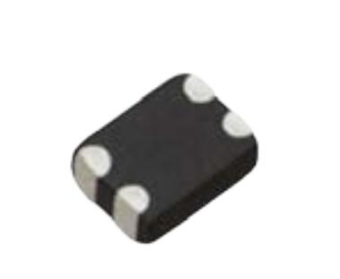


 工商网监
湘ICP备2023018690号
工商网监
湘ICP备2023018690号

