User’s Guide
M0116SY-161MSAR1-C
VFD-RoHS Compliant
(Vacuum Fluorescent Display Module)
*with right angle shrouded connector
For product support, contact
Newhaven Display International
2511 Technology Drive #101
E lgin , IL 601 24
Tel: (847) 8 44-8795
Fax: (847) 8 44-8796
September 28, 2007
Newhaven Display International
M0 116SY-161MSAR1
-C
�STANDARD
NAME
SPECIFICATION FOR APPROVAL
DOCUMENT
NO.
REV.NO
PAGE
00
2/10
1.0 INTRODUCTION
This module is an integrated display module utilizing the D0116SY-20-1601F single row
16 character alpha numeric VFD. An on board converter supplies the DC and AC
voltages necessary to drive the VFD from a single 5V supply. Display driver circuitry
provides character generation for 64 characters as well as 32 dimming levels. Control
of the module is via a simple synchronous serial interface.
2.0
2.1
2.2
2.3
APPLICABLE DOCUMENTS
Engineering Standard Printed Circuit Board Layout criteria.
Vacuum Fluorescent Display Specification Number D0116SY-20-1601F.
Engineering Standard Printed Circuit Board Makings.
3.0 SPECIFICATIONS
3.1
GENERAL SPECIFICATIONS
Item
Value
Number of Characters
16, 1 row
Character Configuration
14 segment alphanumeric
Character Height
5.0mm
Character Width
3.0mm
Character Pitch
5.5mm
Character Tilt
5o
Peak Wavelength
Green(505nm)
Luminance
204 fL typ.
�PART NUMBER:
Newhaven Display International, LLC
3.2
REV:
00
M0116SY-161MSAR1-C
DATE PRINTED:
SHEET:
3 OF 10
MECHANICAL DRAWING
0.18
M0116SY-161MSAR1 HAS
NO CONNECTOR
Figure 1.
NOTES:
3.3
F: filament
Mechanical Drawing (Not to scale)
P: anode
G: grid
NC: No connection
SYSTEM BLOCK DIAGRAM
VFD
FILAMENT
DC - DC/AC
Vcc
GND
DATA
SCLK
RESET
GRID OUTPUTS
ANODE OUTPUTS
DISPLAY DRIVER
Figure 2 . Block Diagram
NP: No pin
�STANDARD
NAME
3.4
DOCUMENT
NO.
SPECIFICATION FOR APPROVAL
REV.NO
PAGE
00
4/10
ENVIRONMENTAL SPECIFICATIONS
Item
Symbol
Min.
Max.
Operating Temperature
Topr
Storage Temperature
Tstg
-50
+95
Relative Humidity (Operating)
Hopr
0
85
%
Relative Humidity (Storage)
Hstg
0
90
%
Vibration (Note 1)
4
G
Shock (Note 2)
40
G
-40
Unit
+85
Notes:
1. Amplitude: 1.5mm; Frequency: 10-55 Hz; Sweep time: 1 min/cycle;
Time: 2 hours/axis (x,y,z).
2. Duration: 11ms; half sine wave; 3 times each (x,y,z).
3.5
ABSOLUTE MAXIMUM ELECTRICAL RATINGS
Item
Symbol
Min.
Max.
Unit
Power Supply Voltage
Vcc
-0.3
+6.5
V
Input Signal voltage
Vin
-0.3
Vcc+0.3
V
3.6 DC ELECTRICAL CHARACTERISTICS
Item
Symbol
Min.
Typ.
Max.
Unit
Power Supply Voltage
Vcc
4.5
5.0
5.5
V
Power Supply Current
Icc
150
200
mA
High Level Input Voltage
Vih
Vcc+0.3
V
High Level Input Current (Vih=5V)
Iih
+10
uA
Low Level Input Voltage
Vil
1.0
V
Low Level Input Current (Vil=0V)
Iil
-0.4
mA
Note:
3.6
0
A surge current of up to 2 times maximum input current can occur upon
power up. The peak surge current amplitude and duration are dependent on
the host power supply characteristics.
�STANDARD
NAME
DOCUMENT
NO.
SPECIFICATION FOR APPROVAL
REV.NO
PAGE
00
5/10
3.7 AC ELECTRICAL CHARACTERISTICS
Item
Symbol
Min.
Max.
Unit
Clock time high
Ton
1.0
20.0
us
Clock time low
Toff
1.0
us
Data Setup Time
Tsu
200
ns
Data Hold Time
Thd
100
ns
Twait
40
us
Byte to Byte Time
Tbb
120
us
Reset time
Trst
100
us
Data ready
Trdy
100
us
Wait between Data words
TIMING DIAGRAMS
Figure 3. SCLK and DATA timing diagram
Figure 4. Byte to Byte timing
Figure 5. Power –up and Reset\timing
�STANDARD
NAME
4.0
SPECIFICATION FOR APPROVAL
DOCUMENT
NO.
REV.NO
PAGE
00
6/10
FUNCTIONAL DESCRIPTION
Input data from the host system is loaded into the module’s display buffer via the
serial data input channel. The internal timing and control system synchronizes the
signal and digit output signals to provide correct timing for the multiplexing
operation. A 16 x 64 bit programmable logic array (PLA) is provided for segment
decoding of the full upper-case ASCII character set. Input data from the host
system is loaded as a series of 8-bit data bytes clocked in on the high to low
transition of the clock.
Control and Character Data Bytes
The most significant bit (bit 7) is loaded first and is referred to as the control bit
(C-bit). If the C-bit of any byte is logical 1, the byte is a control data byte; if it is
logical 0, the byte is a character data byte. The functions and formats of control and
character data bytes are described in detail below.
4.1 WRITING CONTROL DATA BYTES
When the C-bit of the loaded byte is logical 1, it is recognized as a control data
byte. See table below for the format and explanation of each.
8-BIT CONTROL
BYTE
76543210
FUNCTION
1010XXXX
Load Buffer Pointer
(position of character to be defined)
1100YYYY
Load Digit Counter
(number of characters to be displayed)
111ZZZZZ
Load Duty Cycle
(luminance level control)
Notes: 1. “XXXX” – 4 bit binary value of the digit position to be written to
2. “YYYY” – 4 bit binary value of the number of characters to be displayed
3. “ZZZZZ”– 5 bit binary value divided by 31 times 100% equals
luminance level.
�STANDARD
NAME
DOCUMENT
NO.
SPECIFICATION FOR APPROVAL
REV.NO
PAGE
00
7/10
4.1.1
LOAD BUFFER POINTER
The buffer pointer control byte requires bits 7 to 4 to be set to 1010. This allows
any specific character within the display to be modified. The character to be
modified is represented by the value of bits 3 to 0. For a complete list of buffer
pointer values see the table below.
Control
AF
A0
A1
A2
A3
A4
A5
A6
A7
A8
A9
AA
AB
AC
AD
AE
1
2
3
4
5
6
7
8
9
10
11
12
13
14
15
16
Byte
Character
Controlled
For example, to point to character position number 7, a hex value of A5 is entered;
hence, the 8-bit byte would be:
1
0
1
0
0
1
0
1
Position data value.
Buffer pointer control command.
Control data byte identifier.
4.1.2
LOAD DIGIT COUNTER
The digit counter control byte requires bits 7 to 4 to be set to 1100. This is used
to define the number of character positions to be controlled. This byte is
normally used only during initialization routines. The binary value of the data
corresponding to bits 3 to 0 determines the actual number of characters to be
controlled. If less than 16 characters are used, a number corresponding to the
actual number of characters to be controlled should be entered.
For example, if six characters are to be controlled, a hex value of C6 is entered;
hence, the 8-bit byte would be:
1
1
0
0
0
1
1
0
Number of characters to be controlled.
Digit counter control command
Control data byte identifier.
4.1.3
LOAD DUTY CYCLE
The duty cycle control byte requires bits 7 to 5 to be set to 111. The value of the
data corresponding to the remaining bits determines the luminance level of the
display.
�STANDARD
NAME
SPECIFICATION FOR APPROVAL
DOCUMENT
NO.
REV.NO
PAGE
00
8/10
The duty cycle control byte contains a five bit numeric field (bits 4 to 0) that allows
the ‘on’ time for all digits to be modified. Luminance levels are available in 1/32 or
3.1% steps. A value of 31 represents maximum luminance, while a value of 0 places
the output drivers into the “off” state and blanks the display.
For example, a binary value of 24 would force the display’s luminance level to be
77% of maximum luminance, and the full 8-bit byte would be:
1
1
1
1
1
0
0
0
Timing data.
Duty cycle control command.
Control data byte identifier.
4.2 WRITING CHARACTER DATA BYTES
8-BIT DATA BYTE
FUNCTION
0XZZZZZZ
Character Data Byte
NOTES: 1. “X” don’t care
2. “ZZZZZZ” - 6 bit character address from the character table
Character data bytes are loaded into the data buffer as 8 bit bytes, with the C-bit (bit
7) set to 0. The 64 available data bytes are shown in Figure 6, with their
corresponding ASCII characters.
The display buffer pointer is automatically incremented before each character data
byte is stored. Decimal points and commas will not cause the buffer pointer to
increment, and are therefore always associated with the character data byte
previously entered. If it is desirable to place characters out of sequence, that is not
from position 1 to 16, then each character data byte must be preceded by the
appropriate positional data through the use of the buffer pointer control byte.
4.3 POWER-ON RESET
Once Vcc has stabilized after power up, a 100us active low pulse must be applied to
the RESET\ input to initialize the module. The following conditions are established
after a RESET\ pulse has been applied.
�STANDARD
NAME
SPECIFICATION FOR APPROVAL
DOCUMENT
NO.
REV.NO
PAGE
00
9/10
1) The duty cycle is set to 0 (this blanks the display).
2) The digit counter is set to 16 characters.
3) The buffer pointer is set to point to the left most character (position 1).
5.0
INTERFACE CONNECTIOONS
The M0116SY-161MSA1 version of this module has a 10 pin dual row unshrouded header
(DuPont P/N 67996-110).
Pin
Function
Pin
Function
1
Vcc
2
GND
3
SCLK
4
GND
5
DATA
6
GND
7
Reset\
8
GND
9
NC
10
GND
�STANDARD
NAME
Figure 6.
SPECIFICATION FOR APPROVAL
Character Codes
DOCUMENT
NO.
REV.NO
PAGE
00
10/10
�
很抱歉,暂时无法提供与“M0116SY-161MSAR1-C”相匹配的价格&库存,您可以联系我们找货
免费人工找货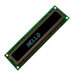


 工商网监
湘ICP备2023018690号
工商网监
湘ICP备2023018690号
