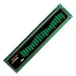
M0121LB‐222LHAR2‐I1
Vacuum Fluorescent Display Module
RoHS Compliant
Newhaven Display International, Inc.
2511 Technology Drive, Suite 101
Elgin IL, 60124
Ph: 847‐844‐8795
Fax: 847‐844‐8796
www.newhavendisplay.com
nhtech@newhavendisplay.com
nhsales@newhavendisplay.com
�STANDARD
NAME
REV .NO
DOCUMENT NO.
PAGE
SPECIFICATION FOR APPROVAL
00
1/16
1. SCOPE
This specification applies to VFD module (Model No: M0121LB-222LHAR2-I1).
2. FEATURES
2.1
2.2
2.3
2.4
2.5
2.6
2.7
This VFD module can be communicated by 8-bit bus systems.
High quality of display and brightness.
Compact and flat packed one-chip controller.
+5V single power supply.
Brightness adjustment available by software (4 levels).
8 user definable fonts available (CG-RAM font).
ASCII characters and LEVEL-BAR patterns (CG-ROM font).
3. GENERAL DESCRIPTIONS
3.1 This specification becomes effective after being approved by the purchaser.
3.2 When any conflict is found in the specification, appropriate action shall be taken upon agreement of
both parties.
3.3 The expected necessary service parts should be arranged by the customer before the completion of
production.
4. PRODUCT SPECIFICATIONS
4.1 Type
Table_1
Type
5
Digit Format
M0121LB-222LHAR2-I1
7 Dot Matrix or 15-Level bar and Icons
4.2 Outer Dimensions, Weight (See Fig-4 for details)
Table_2
Parameter
Width
Height
Thickness
Outer
Dimensions
Weight
Specification
Unit
195.0±1.0
45.0±1.0
Max 25.0
mm
mm
mm
Typical 160
g
�STANDARD
NAME
REV .NO
DOCUMENT NO .
PAGE
SPECIFICATION FOR APPROVAL
00
4.3 Specifications of Display Panel (See Fig-5 for details)
Parameter
D i spl ay S i ze
Table_3
Symbol
Specification
Unit
W ×H
144. 0×18. 0
mm
D i spl ay Pattern D i mensi ons
Display Color
S ee the F i g-5
-
Blue-Green
(peak 505 nm)
Yellowish-Orange (peak 605 nm)
Reddish orange
(peak 665 nm)
-
4.4 Environment Conditions
Parameter
2/16
Table_4
Unit
Symbol
Min.
Max.
Topr
Tstg
4
-20
5
-40
8
+70
9
+85
Operating Temperature
Storage Temperature
Humidity (Operating)
Hopr
0
85
Humidity (Non-operating)
Hstg
0
90
Vibration (10~55Hz)
-
-
4
G
S hock
-
-
40
G
Min.
Max.
Table_5
Unit
4.5 Absolute Maximum Ratings
Parameter
Symbol
Supply Voltage
V CC
-0.5
6.0
V DC
Input Signal Voltage
V IS
-0.5
V CC +0.5
V DC
4.6 Recommend Operating Conditions
Parameter
Symbol
Min.
Typ.
Max.
Table_6
Unit
Supply Voltage
V CC
4.5
5.0
5.5
V DC
Signal (Logic) Input Voltage
V IS
0
-
V CC
V DC
Operating Temperature
T OPR
-20
+25
+70
Min.
Typ.
Max.
I CC
-
600
1000
mA
“H”Level
V IH
0.7×V CC
-
-
V DC
“L”Level
V IL
-
-
0.3×V CC
V DC
V IN =V CC
V IL
20
-
500
uA
100
200
-
10
20
-
17
35
-
4.7 DC Characteristics (Ta=+25 , VCC=+5.0 V
.
Parameter
Symbol
Supply Current *)
Logic Input Voltage
“H” level input current
Green
Brightness
Rsh.O
Ysh.O
L
DC)
Table_7
Unit
ft-L
*) I CC shows the current when all dots are turned on. The surge current can be approx. 3 times
the specified supply current at power on. However, the exact peak surge current amplitude and
duration are dependent on the characteristics of the host power supply.
�STANDARD
NAME
DOCUMENT NO.
REV .NO
PAGE
SPECIFICATION FOR APPROVAL
00
3/16
4.8 Timing Chart and AC Characteristics
4.8.1 Power-on Reset Timing
tr(Vcc)
tOFF(Vcc)
Vcc
Min 100ms
Max 1ms
4.5V
tWAIT*
Min 100us
0.2V
/WR
*Note
tWAIT Internal Reseting Time
Fig-1 Power-on Reset Timing
4.8.2 Data Write-in Timing
RS
tH(RS)
/CS
Min 10ns
tSU(RS)
tCYC(/WR)
Min 10ns
Min 166ns
/WR
tWH(/WR)
Min 100ns
tWL(/WR)
Min 30ns
tSU(data)
tHW(data)
Min 30ns
Min 10ns
VAILD
7
DBO-DB7
Fig-2 Data write-in Timing Diagram
4.9 Connector Pin Assignment
Connector (Male):
BH-S16-FG (by Aster)-16Pin Dual Box Header, Straight
Male Socket(Female):MIL-STD-16P
#15
#1
#16
#2
*NC : No Connection
No
Signal
No
Signal
1
DB7
2
DB6
3
DB5
4
DB4
5
DB3
6
DB2
7
DB1
8
DB0
9
/WR
10
/CS
11
RS
12
*NC
13
Vcc
14
Vcc
15
GND
16
GND
�STANDARD
NAME
DOCUMENT NO.
REV .NO
PAGE
SPECIFICATION FOR APPROVAL
00
4/16
4.10 System Block Diagram
Vcc
VDD
Controller
#11
RS
/CS
#10
/CS
/WR
#9
RS
/WR
73 Lines
ANODE
22 Lines
GRID
VFD
33-2201F
DB0-DB7
VDISP
#1-#8
Vcc #13,14
(+5Vdc)
GND
#15,16
DC/DC
Converter
Vbb
Ef1
Ef2
Fig-3 System Block Diagram of this VFD Module
4.11 Outer Dimensions
Fig-4 Outer Dimensions
F1
F2
�STANDARD
NAME
DOCUMENT NO.
REV .NO
PAGE
SPECIFICATION FOR APPROVAL
4.12 Pattern Details
00
5/16
�DOCUMENT NO.
STANDARD
NAME
REV .NO
PAGE
SPECIFICATION FOR APPROVAL
00
6/16
5. FUNCTION DESCRIPTIONS
5.1 Registers in VFD Controller
The VFD controller has two 8-bit registers, an instruction register (IR) and a data register (DR).
IR stores instruction codes, such as display clear and address information for DD-RAM and CG-RAM.
The IR can only be written from the host MPU. DR temporarily stores data to be written into DD-RAM
or CG-RAM.
Data written into the DR from the MPU is automatically written into DD-RAM or CG-RAM by
an internal operation.
By the register selector (RS) signal, these two registers can be selected (See Table_8).
Table_8 Register Selection
RS
/CS
/WR
Operation
0
0
0 to 1
IR write as an internal operation (display clear, etc.)
1
0
0 to 1
DR write as an internal operation (DR to DDRAM or CGRAM)
×: Don’t care
5.1.1 Address Counter (ACC)
The address counter (ACC) assigns addresses to both DD-RAM and CG-RAM. When an address
Of an instruction is written into the IR, the address information is sent from the IR to the ACC.
Selection of either DD-RAM or CG-RAM is also determined concurrently by the instruction.
After writing into DD-RAM or CG-RAM, the ACC is automatically incremented by 1
( decremented by 1).
5.1.2 Display Data RAM (DD-RAM)
Display data RAM (DD-RAM) stores display data represented in 8-bit character codes.
The area in DD-RAM that is not used for display can be used as general data RAM.
See Table_9 for the relationships between DD-RAM addresses and positions on the VFD.
Table_9 Relation between Digit Position and DD-RAM data
Digit
G1
G2
G3
G21
G22
Upper Row code
00Hex
01Hex
02Hex
14Hex
15Hex
Lower Row code
40Hex
41Hex
42Hex
54Hex
55Hex
5.1.3 Character Generator ROM (CG-RAM)
The character generator ROM (CG-ROM) generates character patterns of 5×7 dots from 8-bit
Character codes (Table-10). It can generate 112 kinds of 5×7 dot character patterns and 64
kinds of level bar patterns.
The character fonts are shown on the following page. The character coders 00Hex to 0Fhex
are allocated to the CG-RAM.
��REV .NO
DOCUMENT NO.
STANDARD
NAME
PAGE
SPECIFICATION FOR APPROVAL
00
8/16
Table_11 Relationship between CG-RAM Addresses, Character Codes (DD-RAM) and 5×7 (with Cursor)
Dot Character Patterns (CG-RAM data)
Character Codes
(DD-RAM data)
D
7
0
0
0
D
6
0
0
0
D
5
0
0
0
D
4
0
0
0
D
3
×
×
×
D
2
0
0
1
Character Patterns
CG-RAM Address
D
1
0
0
1
(CG-RAM data)
D
D
D
D
D
D
D
D
2
1
0
7
6
5
4
3
2
1
0
0
0
0
×
×
×
1
2
3
4
5
0
0
1
×
×
×
6
7
8
9
10
or
D
A A A A A A
0
5
0
1
1
0
0
1
4
0
0
1
3
0
1
1
Character
Level
0
1
0
×
×
×
11
12
13
14
15
bar Pattern
0
1
1
×
×
×
16
17
18
19
20
(1)
1
0
0
×
×
×
21
22
23
24
25
1
0
1
×
×
×
26
27
28
29
30
1
1
0
×
×
×
31
32
33
34
35
1
1
1
×
×
×
36
37
38
×
×
0
0
0
×
×
×
1
2
3
4
5
0
0
1
×
×
×
6
7
8
9
10
or
0
1
0
×
×
×
11
12
13
14
15
bar
0
1
1
×
×
×
16
17
18
19
20
Pattern
1
0
0
×
×
×
21
22
23
24
25
(2)
1
0
1
×
×
×
26
27
28
29
30
1
1
0
×
×
×
31
32
33
34
35
1
1
1
×
×
×
36
37
38
×
×
0
0
0
×
×
×
1
2
3
4
5
0
0
1
×
×
×
6
7
8
9
10
or
0
1
0
×
×
×
11
12
13
14
15
bar
0
1
1
×
×
×
16
17
18
19
20
Pattern
1
0
0
×
×
×
21
22
23
24
25
(8)
1
0
1
×
×
×
26
27
28
29
30
1
1
0
×
×
×
31
32
33
34
35
1
1
1
×
×
×
36
37
38
×
×
Character
Level
Character
Level
Notes: 1.Character code bits 0 to 2 correspond to CG-RAM address bits 3 to 5 (3 bits: 8 types)
2.CG-RAM address bits 0 to 2 designate the character pattern line position. The 8th line is
composed of the Center Level bar (36: Center Bar), Icons (37: S1+S2 38: S18).
3. Character pattern row positions correspond to CG-RAM data bits 0 to 4 (bit 4 being at the left).
4. As shown Table_11,CG-RAM character patterns are selected when character codes bits 4 to 7
are all 0. However, since character codes bit 3 has no effect, the display example above can be
selected by either character code 00H or 08H.
5. 1 for CG-RAM data corresponds to display selection and 0 to non-selection.
“×” Indicates no effect (Don’t care)
�STANDARD
NAME
REV .NO
DOCUMENT NO.
PAGE
SPECIFICATION FOR APPROVAL
00
9/16
5.1.4 Character Generator RAM (CG-RAM)
In the character generator RAM (CG-RAM), the user can rewrite character patterns by program.
Indicator icons of G1 must be written CG-RAM.
Also 5×7 dots or level bars patterns can be written CG-RAM.
Write into DD-RAM the character codes at the addresses shown as the left column of Table-10
to show the character patterns shored in CG-RAM.
See Table-11 for the relationship between CG-RAM addresses and data and display patterns
and refer to Fig-6 for dot assignment of VFD.
Areas that are not used for display can be used as general data RAM.
1) CG-RAM Assignment for G1
1
2
3
4
5
1
2
3
4
5
(S3)
×
×
×
×
×
×
×
×
×
6
7
8
9
10
6
7
8
9
10
×
×
×
×
×
×
×
×
×
×
14
15
11
12
13
14
15
11
12
13
(S4)
×
×
×
×
×
×
(S16)
×
×
16
17
18
19
20
16
17
18
19
20
(S5)
×
×
×
(S6)
×
×
×
×
×
21
22
23
24
25
21
22
23
24
25
×
×
×
×
(S7)
×
×
×
×
×
27
28
29
30
26
27
28
29
30
26
(S8)
(S9)
×
×
×
(S15)
(S14)
(S13)
×
×
31
32
33
34
35
31
32
33
34
35
×
×
×
×
×
×
×
×
(S12)
(S11)
36
37
38
39
40
36
37
38
39
40
×
×
×
(S17)
×
×
(S10)
×
×
×
[Upper Row]
Fig-7 Icons Assignment
2) CG-RAM for 5×7 Dot and S1, S2, S18 icons
Refer to Table_11
[Lower Row]
�STANDARD
NAME
DOCUMENT NO.
REV .NO
PAGE
SPECIFICATION FOR APPROVAL
00
10/16
5.2 Interfacing to the MPU
This VFD module can interface in 8-bit operation.
5.3 Power-on reset
An internal reset circuit automatically initializes the module when the power is turned on.
The following instructions are executed during the initialization.
1) Display clear
Fill the DD-RAM with 20H(Space Code)
2) Set the address counter to 00H
Set the address counter (ACC) to point DD-RAM.
3) Display on/off control:
D=0
: Display off
B=0
: Blinking off
4) Entry mode set:
I/D = 1
: Increment by 1
S =0
: No shift
5) Function Set
IF = 1
: 8-bit interface data
N=1
: 2-line display
BR0 = BR1 = 0 ; Brightness = 100
6. INSTRUCTIONS
6.1 Outline
Only the instruction register (IR) and the data register (DR) of the VFD controller can be controlled by
the user’s MPU. Before starting the internal operation of the controller, control information is temporarily
stored into these registers to allow interfacing with various MPUs, which operate at different speeds, or
various peripheral control devices. The internal operation of the controller is determined by signals sent
from the MPU. These signals, which include register selection signal (RS), write signal (/WR) and the
data bus (DB0 to DB7), make up the controller instructions (See Table_13).
These are four categories of instructions that:
.Designate controller functions, such as display format, data length, etc.
.Set internal RAM addresses
.Perform data transfer with internal RAM
.Perform miscellaneous functions
Normally, instructions that perform data transfer with internal RAM are used the most.
However, auto-incrementation by 1 ( or auto-decrementation by 1) of internal RAM addresses after each
data write can lighten the program load of the MPU. Since the display shift instruction can perform
concurrently with display data write, the user can minimize system development time with maximum
programming efficiency.
�STANDARD
NAME
REV .NO
DOCUMENT NO.
PAGE
SPECIFICATION FOR APPROVAL
00
11/16
Table _13 Instruction Set
CODE
Instruction
Display Clear
Cursor Home
Entry Mode Set
DB
DB
DB
DB
DB
DB
DB
DB
R
7
6
5
4
3
2
1
0
0
0
0
0
0
0
0
1
Clear all display and sets DD-RAM
address 0 in address counter
×
Sets DD-RAM address 0 in ACC.
Also returns the display being shifted
to the original position. DD-RAM
contents remain unchanged
S
Specify display shift.
These operations are
during writing data.
C
B
Sets all display ON/OFF (D), cursor
ON/OFF(C), Cursor blink of
character position (B).
×
×
Shifts display keeping DD-RAM
contents.
BR
BR
1
0
RS
0
0
0
0
0
0
0
0
0
0
0
Display
ON/OFF
Control
0
0
0
0
0
Cursor or
Display Shift
0
0
0
0
1
Function Set
0
CGRAM
Address Setting
0
0
DDRAM
Address Setting
0
1
Data Writing to
CG or DDRAM
1
*NOTE
Description
/W
0
0
1
1
1
0
0
1
1
D
S/
R/
C
L
N
×
ACG
ADD
Data writing
I/D =1 : Increment
I/D =0 : Decrement
S = 1 : Display shift enabled
S = 0 : Display shift disabled
S/C = 1: Display shift
S/C = 0: Ignore
R/L = 1: Shift to the right
R/L = 0: Shift to the left
IF = 1: 8bits
IF = 0: 4bits
N = 1 : 2 lines display
N = 0 : 1 line display
BR1, BR0 = 00 : 100% 01: 75%
10 : 50% 11: 25%
×: Don’t Care
0
1
I/D
performed
Sets number of display lines (N), Set
Brightness level (BR1, BR0)
Sets the CG-RAM address.
Sets the DD-RAM address.
Writes data
DD-RAM.
into
CG-RAM
[ Abbreviation]
DD-RAM : Display Data RAM
CG-RAM : Character Generator
RAM
ACG : CG-RAM Address
ADD : DD-RAM Address
ACC : Address Counter
or
�DOCUMENT NO.
STANDARD
NAME
REV .NO
PAGE
SPECIFICATION FOR APPROVAL
00
12/16
6.2 Instruction Descriptions
6.2.1 Display Clear
DB7
DB6
DB5
DB4
DB3
DB2
DB1
DB0
0
0
0
0
0
0
0
1
01H
RS=0, /CS= 0, /WR= 0 to 1
This instruction
(1) Fills all locations in the display data RAM (DD-RAM) with 20H (Blank-character).
(2) Clear the contents of the address counter (ACC) to 00H.
(3) Sets the display for zero character shift (returns original position).
(4) Sets the address counter (ACC) to point to the DD-RAM.
(5) Sets the address counter (ACC) to increment on the each access of DD-RAM or CG-RAM.
6.2.2 Cursor Home
DB7
DB6
0
0
DB5
0
DB4
0
DB3
DB2
DB1
DB0
0
0
1
×
02H to 03H
× : Don’t care
RS=0, /CS= 0, /WR= 0 to 1
This instruction
(1) Clear the contents of the address counter (ACC) to 00H.
(2) Sets the address counter (ACC) to point to the DD-RAM.
(3) Sets the display for zero character shift (returns original position).
6.2.3 Entry Mode Set
DB7
0
DB6
DB5
DB4
DB3
DB2
DB1
0
0
0
0
1
I/D
DB0
S
04H to 07H
RS=0, /CS= 0, /WR= 0 to 1
The I/D bit selects the way in which the contents of the address counter (ACC) are modified after
every access to DD-RAM or CG-RAM.
I/D = 1 : The address counter (ACC) is incremented.
I/D = 0 : The address counter (ACC )is decremented.
The S bit enables display shift, instead of cursor shift, after each write or read to the DD-RAM.
S = 1 : Display shift enabled.
S = 0 : Cursor shift enabled.
The direction in which the display is shifted is opposite in sense to that of the cursor.
For example, if S=0 and I/D=1,the cursor would shift one character to the right after a MPU writes to
DD-RAM. However if S=1 and I/D=1, the display would shift one character to the left and the cursor
would maintain its position on the panel.
�DOCUMENT NO.
STANDARD
NAME
REV .NO
PAGE
SPECIFICATION FOR APPROVAL
00
13/16
The cursor will already be shifted in the direction selected by I/D during reads of DD-RAM,
Irrespective of the value of S. Similarly reading and writing the CG-RAM always shift the cursor.
Also both lines are shifted simultaneously.
Table_14 Cursor move and Display shift by the “Entry Mode Set”
I/D
S
0
0
The cursor moves one character to the left.
After writing DD-RAM data
The cursor moves one character to the left.
After Reading DD-RAM data
1
0
The cursor moves one character to the right.
The cursor moves one character to the right.
0
1
The display shifts one character to the right
without cursor’s move.
The cursor moves one character to the left.
1
1
The display shifts one character to the left
without cursor’s move.
The cursor moves one character to the right.
6.2.4 Display ON/OFF
DB7
DB6
DB5
DB4
DB3
0
0
0
0
1
DB2
DB1
DB0
D
C
B
08H to 0FH
RS=0, /CS=0, /WR=0 to 1
This instruction controls various features of display.
D = 1 : Display on,
D = 0 : Display off.
C = 1 : Cursor on,
C = 0 : Cursor off.
B = 0 : Blinking off.
B = 1 : Blinking on
(Blinking is achieved by alternating between a normal and all on display of a character.
The cursor blinks with a frequency of about 1.0 HZ and DUTY 50%.)
6.2.5 Display Shift
DB7
DB6
DB5
DB4
DB3
DB2
DB1
DB0
0
0
0
1
S/C
R/L
×
×
10H to 1FH
× : Don’t care
RS=0, /CS=0, /WR=0 to 1
This instruction shifts the display moves one character to the left or right, without writing DD-RAM.
The S/C bit selects movement of the display.
S/C = 1 : Shift display
S/C = 0 : No shift display
The R/L bit selects left ward or right ward movement of the display and/or cursor.
R/L = 1 : Shift one character right
R/L = 0 : Shift one character left
�DOCUMENT NO.
STANDARD
NAME
REV .NO
PAGE
SPECIFICATION FOR APPROVAL
00
14/16
Table_15 Cursor/Display shift
S/C
R/L
Cursor shift
Display shift
0
0
Move one character to the left
No shift
0
1
Move one character to the right
No shift
1
0
Shift one character to the left with display
Shift one character to the left
1
1
Shift one character to the right with display
Shift one character to the right
6.2.6 Function Set
DB7
DB6
0
0
DB5
1
DB4
DB3
DB2
1
N
×
DB1
BR1
DB0
BR0
20H to 3FH
× : Don’t care
RS=0, /CS=0, /WR=0 to 1
This instruction initializes the system, and must be the first instruction executed after power-on.
The N bit selects between 1-line or 2-line display.
N = 1 : Select 2 line display( Using anode output A1 to A80)
N = 0 : Select 1 line display (Using anode output A1 to A40. A41 to A80 fixed Low level.)
BR1, BR0 flag is control to brightness of VFD to modulate pulse width of Anode output as follows.
BR1
BR0
Brightness
0
0
100%
0
1
75%
1
0
50%
1
1
25%
6.2.7 Set CG-RAM Address
DB7
0
DB6
DB5
DB4
DB3
1
DB2
DB1
DB0
40H to 7FH
ACG
RS=0, /CS=0, /WR=0 to 1
This instruction
(1) Load a new 6-bit address into the address counter (ACC).
(2) Sets the address counter (ACC) to address CG-RAM.
Once “Set CG-RAM Address” has been executed, the contents of the address counter (ACC) will be
automatically modified after every access of CG-RAM, as determined by the “Entry Mode Set” instruction.
The active width of the address counter (ACC), when it is addressing CG-RAM, is 6 bits, so the counter
will wrap around to 00H from 3FH if more than 64 bytes of data are written to CG-RAM.
6.2.8 Set DD-RAM Address
DB7
DB6
DB5
DB4
1
RS=0, /CS=0, /WR=0 to 1
DB3
ADD
DB2
DB1
DB0
80H to AFH (1-line)
C0H to E7H (2-line)
�DOCUMENT NO.
STANDARD
NAME
REV .NO
PAGE
SPECIFICATION FOR APPROVAL
00
15/16
This instruction
(1) Loads a new 7-bit address into the address counter (ACC).
(2) Sets the address counter (ACC) to point to the DD-RAM.
Once the “Set DD-RAM Address” instruction has been executed. The contents of the address counter
(ACC) will be automatically modified after each access of DD-RAM, as selected by the “Entry Mode Set”
instruction.
Table_16 Valid DD-RAM address Ranges
Number of character
Address Range
1st line
40
00H to 27H
2nd
40
40H to 67H
line
6.2.9 Write Data to CG or DD-RAM
DB7
DB6
DB5
DB4
DB3
DB2
DB1
DB0
Data Write
00H to FFH
RS=1, /CS=0, /WR=0 to 1
This instruction writes 8-bit binary data (DB7 to DB0) into CG-RAM or DD-RAM.
To write into CG-RAM or DD-RAM is determined by the pervious specification of the CG-RAM or
DD-RAM address setting. After a write, the address is automatically incremented or decremented by 1
according to the entry mode. The entry mode also determines the display shift.
When data is written to the CG-RAM, the DB7, DB6 and DB5 bits are not displayed as characters.
7. Example of the Display Data Writing
Display data sheet of table_14 lists Display pattern of Fig-9
Fig-9 Display pattern Example
�STANDARD
NAME
DOCUMENT NO.
REV .NO
PAGE
SPECIFICATION FOR APPROVAL
00
16/16
If a user wants to display above pattern then please make following procedures.
1. Power on
2. Wait more than 15ms after Vcc rise to 4.5V.
3. Function set (RS=0, Data =38h to assign 2-line display)
4. Display On (RS=0,Data =0Ch to assign Display On, Cursor off and Blinking off)
5. CG-RAM Address Set (RS = 0,Data = 00h to assign the first CG-RAM address)
6. CG-RAM Data Write-in (RS = 1,Data =10h + 00h + 00h + 10h + 18h + 00h + 00h)
7. CG-RAM Address Set (RS=0,Data=01h to assign the second CG-RAM address)
8. CG-RAM Data Write-in (RS = 1,Data = 00h + 00h + 04h + 00h + 00h + 08h + 01h + 00h)
9. DD-RAM Address Set (RS = 0,Data=80h to assign the Upper Icons which are located in G1)
10. CG-RAM data write-in on Upper Icon of G1 (RS=1, Data =00h)
11. DD-RAM Address Set (RS = 0,Data=C0h to assign the Lower Icons which are located in G1)
12. CG-RAM data write-in on Lower Icon of G1 (RS=1,Data=01h)
13. DD-RAM Address Set (RS = 0,DATA=81h to assign the Upper Line of G2)
14. CG-ROM data write-in (RS =1,Data = 38h + 82h + 87h +[16 CG-ROM codes] + E1H + 99h)
15. DD-RAM Address Set (RS = 0,DATA=C1h to assign the Lower Line of G2)
16. CG-ROM data write-in (RS =1,Data = 4Dh + FEh + BEh +[16 CG-ROM codes] + F1H + A8h)
8.OPERATING RECOMMENDATIONS
8.1 Avoid applying excessive shock or vibration beyond the specification for the VFD module.
8.2 Since VFDs are made of glass material, careful handling is required.
i.e. Direct impact with hard material to the glass surface (especially exhaust tip)may crack the glass.
8.3 When mounting the VFD module to your system, leave a slight gap between the VFD glass and your
front panel. The module should be mounted without stress to avoid flexing the PCB.
8.4 Avoid plugging or unplugging the interface connection with the power on, otherwise it may cause the
severe damage to input circuitry.
8.5 Slow starting power supply may cause non-operation because one chip micom won’t be reset.
8.6 Exceeding any of maximum ratings may cause the permanent damage.
8.7 Since the VFD modules contain high voltage source, careful handling is required during powered on.
8.8 when the power is turned off, the capacitor does not discharge immediately.
The high voltage applied to the VFD must not contact to the ICs. And the short-circuit of mounted
Components on PCB within 30 seconds after power-off may cause damage to those.
8.9 The power supply must be capable of providing at least 3 times the rated current, because the surge
current can be more than 3 times the specified current consumption when the power is turned on.
8.10 Avoid using the module where excessive noise interference is expected. Noise may affect the interface
signal and causes improper operation. And it is important to keep the length of the interface cable less
than 50cm.
8.11 Since all VFD modules contain C-MOS ICs, anti-static handling procedures are always required.
�


 工商网监
湘ICP备2023018690号
工商网监
湘ICP备2023018690号
