NHD-5.0-800480TF-ATXI#-CTP 数据手册
N
NHD‐‐5.0‐‐8004
480TTF‐A
ATXI##‐CTTP
TFTT (Thin‐‐Film‐Trransisto
or) Colo
or Liquid
d Crystaal Displlay Mod
dule
NHD‐‐
5.0‐
8004
480‐
TF‐
A‐
T‐
X‐
I‐
#‐
CTP‐
Newhaven Display
5.0” Diagonal
80
00xRGBx480 pixels
Model
M
Built‐in driver / NO Controller
White LED bac
W
cklight
TFT
6:00 viewing angle, Wide Te
emp
RoHS Compliant
Capacitive touch panel with
h controller
Newh
haven Disp
play Intern
national, In
nc.
2511 Techno
ology Drive, SSuite 101
Elggin IL, 60124
Ph: 8
847‐844‐8795
5
Fax: 8847‐844‐87966
www.new
whavendisplayy.com
nhtech
h@newhaven
ndisplay.com
nhsaales@newhavvendisplay.co
om
�Document Revision History
Revision
0
1
2
Date
2/1/2012
3/18/2013
8/5/2013
Description
Initial Release
Timing Characteristics added
Optical characteristics updated
Functions and Features
800xRGBx480 resolution, up to 16.7M colors
14‐LED backlight
24 bit RGB interface
Capacitive Touch Panel with Controller
[2]
Changed by
SB
AK
ML
�L
A
I
Mechanical Drawing
2
3
120.70±0.2 (TFT Outline)
109.00 (TFT V.A.)
108.00 (TFT A.A.)
4
3.10 (TFT)
A
T
N
E
D
I
40
54.25±1
B
O
C
Detail: B
Front View
2(0.50±0.10)
1
C
5±0.3
Stiffener
61±1
46.0
23.0
F
N
43.0
1
C
1.5MAX
3±0.3
Conductive plate
B
D
Adhesive
0.1mm
65.80 (CTP A.A.)
75.80 (CTP Outline)
75.8±0.20 (TFT Outline)
65.80 (TFT V.A.)
64.80 (TFT A.A.)
A
0.3±0.05
Date
0.135
0.043
A
Detail: C
Rear View
B
W=0.5±0.05
*P:1.0X(6-1)=5±0.05
6.5±0.1
1.30 Max
C
0.3±0.03
Side View (TFT)
Side View (CTP)
D
w=0.35±0.03
Date
p=0.50±0.03
03/18/13
P0.5x(40-1)=19.50±0.05
20.50±0.7
2
6
Description
Enlarged to show detail
1.2±0.1
117.60±0.1 (CTP Outline)
109.00 (CTP A.A.)
70.0
5
Rev
0.135
1
Unit
Gen. Tolerance
±0.3mm
3
4
mm
5
Model:
NHD-5.0-800480TF-ATXI#-CTP
6
The drawing contained herein is the exclusive property of Newhaven Display International, Inc. and shall not be copied, reproduced, and/or disclosed in any format without permission.
[3]
�Pin Description
TFT:
Pin No. Symbol
1
2
3
4
5‐12
13‐20
21‐28
29
30
31
32
33
34
35
36
37
38
39
40
LED‐
LED+
GND
VDD
[R0‐R7]
[G0‐G7]
[B0‐B7]
GND
CLKIN
STBYB
HSYNC
VSYNC
DEN
NC
GND
XR
YD
XL
YU
External
Connection
LED Power Supply
LED Power Supply
Power Supply
Power Supply
MPU
MPU
MPU
Power Supply
MPU
MPU
MPU
MPU
MPU
‐
Power Supply
‐
‐
‐
‐
Function Description
Ground for Backlight
Backlight Power Supply (20mA @ 23.1V)
Ground
Power supply for LCD and logic (3.3V)
Red Data Signals
Green Data Signals
Blue Data Signals
Ground
Clock for input data (Rising Edge)
1: Normal Operation; 0: Standby Mode
Line synchronization signal
Frame synchronization signal
Data Enable signal
No Connect
Ground
No Connect
No Connect
No Connect
No Connect
Recommended LCD connector: 0.5mm pitch 40‐Conductor FFC. Molex p/n: 54104‐4031 (top contact)
Backlight connector: on LCD connector
Mates with: ‐‐‐
Capacitive Touch Panel:
Pin No. Symbol
1
2
3
4
5
6
VCC
GND
SCL
SDA
/INT
/WAKE
External
Connection
Power Supply
Power Supply
MPU
MPU
MPU
MPU
Function Description
Power supply for logic (3.0V)
Ground
Serial I2C Clock (Requires pull‐up resistor)
Serial I2C Data (Requires pull‐up resistor)
Interrupt signal from touch panel module to host
External interrupt signal from host (0: Disable /INT 1: Enable /INT)
Recommended connector: 1.0mm pitch 6‐Conductor FFC. Molex p/n: 52271‐0679
Driver/Controller Information
TFT:
Built‐in HX8264‐D02 Source Driver: http://www.newhavendisplay.com/app_notes/HX8264‐D02.pdf
Built in HX8664‐B Gate Driver: http://www.newhavendisplay.com/app_notes/HX8664‐B.pdf
Capacitive Touch Panel:
Built‐in FocalTech FT5x06 controller.
Please download specification at http://www.newhavendisplay.com/app_notes/FT5x06.pdf
[4]
�Electrical Characteristics
TFT:
Item
Operating Temperature Range
Storage Temperature Range
Supply Voltage
Supply Current
“H” Level input
“L” Level input
“H” Level output
“L” Level output
Backlight Supply Voltage
Backlight Supply Current
Backlight Power Consumption
Symbol
Top
Tst
VDD
IDD
Vih
Vil
Voh
Vol
VLED
ILED
PBL
Condition
Absolute Max
Absolute Max
VDD=3.3
Min.
‐20
‐30
3.0
‐
0.7*VDD
VSS
VDD‐0.4
VSS
Typ.
‐
‐
3.3
132
‐
‐
‐
‐
‐
‐
‐
23.1
20
924
Max.
+70
+80
3.6
‐
VDD
0.3*VDD
VDD
VSS+0.4
‐
25
‐
Unit
⁰C
⁰C
V
mA
V
V
V
V
V
mA
mW
Max.
+70
+80
3.3
‐
‐
VDD
0.3*VDD
VDD
0.3*VDD
Unit
⁰C
⁰C
V
mA
mA
V
V
V
V
Max.
‐
‐
‐
‐
‐
‐
30
Unit
⁰
⁰
⁰
⁰
cd/m2
ms
Capacitive Touch Panel:
Item
Operating Temperature Range
Storage Temperature Range
Supply Voltage
Supply Current – Operating
Supply Current – Hibernate
“H” Level input
“L” Level input
“H” Level output
“L” Level output
Symbol
Top
Tst
VDD
IDD
IDD
Vih
Vil
Voh
Vol
Condition
Absolute Max
Absolute Max
Ta=25°C, VDD=2.8V
Ta=25°C, VDD=2.8V
Min.
‐20
‐30
2.8
‐
‐
0.7*VDD
VSS
0.7*VDD
VSS
Typ.
‐
‐
‐
6.0
0.03
‐
‐
‐
‐
Optical Characteristics:
Item
Viewing Angle –Top
Viewing Angle –Bottom
Viewing Angle – Left
Viewing Angle – Right
Contrast Ratio
Luminance
Response Time
Symbol
Cr
YL
Tr+Tf
Condition
Cr 10
‐
Min.
‐
‐
‐
‐
500
‐
‐
Capacitive Touch Panel Material Characteristics:
Property
IC
Glass thickness
Top film thickness
Surface Hardness
Light transmission
Operating Humidity
Storage Humidity
Requirement
FT5306DE3
0.7
0.125
6(750)
82%
45~85
5~95
Unit
mm
mm
H(g)
‐
RH
RH
[5]
Typ.
50
70
70
70
600
250
20
�Tim
ming Charracteristiccs
[6]
�Horiizontal Tim
ming
Verttical Timingg
[7]
�Paraallel 24‐bit RGB mode
ut Clock and
d Data Timing
Inpu
Sourrce Output Timing
[8]
�Verttical Timingg HV (Casca
ade)
Verttical Timingg DE (Cascade)
Gatee Output Tiiming
[9]
�Verttical Timingg HV (Dual G
Gate)
Gate)
Verttical Timingg DE (Dual G
Gatee Output Tiiming (Dual Gate)
[10]
�Pow
wer ON/O
OFF Sequence
Entter/Exit Standby M
Mode Seq
quence
[11]
�Capacitive Touch registers:
Address Name
B7
B6
B5
B4
00h
DEVICE_MODE
01h
GEST_ID
02h
TD_STATUS
03h
TOUCH1_XH
Event Flag
04h
TOUCH1_XL
1st Touch X Position LSB [7..0]
05h
TOUCH1_YH
Touch ID [3..0]
06h
TOUCH1_YL
1st Touch Y Position LSB [7..0]
B3
B2
B1
B0
Device Mode [2..0]
R/W
Gesture ID [7..0]
R
Touch Points [3..0]
1st Touch X Position MSB [11..8]
1st Touch Y Position MSB [11..8]
R
R
R
R
R
09h
TOUCH2_XH
Event Flag
2nd Touch X Position MSB [11..8]
0Ah
TOUCH2_XL
2nd Touch X Position LSB [7..0]
0Bh
TOUCH2_YH
Touch ID [3..0]
0Ch
TOUCH2_YL
2nd Touch Y Position LSB [7..0]
R
R
2nd Touch Y Position MSB [11..8]
R
R
0Dh
0Eh
R
R
0Fh
TOUCH3_XH
Event Flag
3rd Touch X Position MSB [11..8]
10h
TOUCH3_XL
3rd Touch X Position LSB [7..0]
11h
TOUCH3_YH
Touch ID [3..0]
12h
TOUCH3_YL
3rd Touch Y Position LSB [7..0]
R
R
3rd Touch Y Position MSB [11..8]
R
R
13h
14h
R
R
15h
TOUCH4_XH
Event Flag
4th Touch X Position MSB [11..8]
16h
TOUCH4_XL
4th Touch X Position LSB [7..0]
17h
TOUCH4_YH
Touch ID [3..0]
18h
TOUCH4_YL
4th Touch Y Position LSB [7..0]
R
R
4th Touch Y Position MSB [11..8]
R
R
19h
1Ah
R
R
1Bh
TOUCH5_XH
Event Flag
5th Touch X Position MSB [11..8]
1Ch
TOUCH5_XL
5th Touch X Position LSB [7..0]
1Dh
TOUCH5_YH
Touch ID [3..0]
1Eh
TOUCH5_YL
5th Touch Y Position LSB [7..0]
R
R
5th Touch Y Position MSB [11..8]
1Fh
R
R
R
[12]
R
R
07h
08h
Access
�
Address Name
B7
B6
B5
B4
B3
B2
B1
80h
ID_G_THGROUP
valid touching detect threshold
R/W
81h
ID_G_THPEAK
valid touching peak detect threshold
R/W
82h
ID_G_THCAL
the threshold when calculating the focus of touching
R/W
83h
ID_G_THWATER
the threshold when there is surface water
R/W
84h
ID_G_TEMP
the threshold of temperature compensation
R/W
85h
ID_G_THDIFF
the threshold whether the coordinate is different from original
R/W
86h
ID_G_CTRL
Power Control Mode [1..0]
R/W
87h
ID_G_TIME_ENTER_MONITOR the timer for entering monitor status
R/W
88h
ID_G_PERIODACTIVE
R/W
89h
ID_G_PERIODMONITOR
the timer of entering idle when in monitor status
R/W
A0h
ID_G_AUTO_CLB_MODE
auto calibration mode
R/W
A1h
ID_G_LIB_VERSION_H
Firmware Library Version H byte
R
A2h
ID_G_LIB_VERSION_L
Firmware Library Version L byte
R
A3h
ID_G_CIPHER
Chip vendor ID
R
A4h
ID_G_MODE
the interrupt status to host
R
A5h
ID_G_PMODE
Power Consume Mode
A6h
ID_G_FIRMID
Firmware ID
A7h
ID_G_STATE
Running State
A8h
ID_G_FT5201ID
CTPM Vendor ID
R
A9h
ID_G_ERR
Error Code
R
AAh
ID_G_CLB
Configure TP module during calibration in Test Mode
R/W
FEh
LOG_MSG_CNT
The log MSG count
R
FFh
LOG_CUR_CHA
Current character of log message
R
Period Active [3..0]
B0
Access
R
NOTE: Registers 80h – AFh have been configured for optimum settings and do not need to be modified.
[13]
�Capacitive Touch Register Description:
Register No
00h
Register Name
Device Mode
Bits
[2:0]
Value
000b
Description
Normal Operating Mode
100b
Test Mode ‐ read raw data (reserved)
01h
Gesture ID
[7:0]
001b
48h
System Information Mode (reserved)
Zoom In
49h
Zoom Out
00h
No Gesture
02h
Touch Points
[3:0]
000b
0 touch points detected
001b
1 touch point detected
010b
2 touch points detected
011b
3 touch points detected
100b
4 touch points detected
101b
5 touch points detected
03h
Touch 1 Event Flag
[7:6]
00b
Put Down
01b
Put Up
10b
Contact
11b
Reserved
03h
TOUCH1_XH
[3:0]
0h ‐ 3h
Upper 4 bits of X touch coordinate
04h
TOUCH1_XL
[7:0]
00h ‐ FFh
Lower 8 bits of X touch coordinate
05h
TOUCH1_YH
[3:0]
0h ‐ 1h
Upper 4 bits of Y touch coordinate
06h
TOUCH1_YL
[7:0]
00h ‐ FFh
Lower 8 bits of Y touch coordinate
09h
Touch 2 Event Flag
[7:6]
00b
Put Down
01b
Put Up
10b
Contact
11b
Reserved
09h
TOUCH2_XH
[3:0]
0h ‐ 3h
Upper 4 bits of X touch coordinate
0Ah
TOUCH2_XL
[7:0]
00h ‐ FFh
Lower 8 bits of X touch coordinate
0Bh
TOUCH2_YH
[3:0]
0h ‐ 1h
Upper 4 bits of Y touch coordinate
0Ch
TOUCH2_YL
[7:0]
00h ‐ FFh
Lower 8 bits of Y touch coordinate
0Fh
Touch 3 Event Flag
[7:6]
00b
Put Down
01b
Put Up
10b
Contact
11b
Reserved
0Fh
TOUCH3_XH
[3:0]
0h ‐ 3h
Upper 4 bits of X touch coordinate
10h
TOUCH3_XL
[7:0]
00h ‐ FFh
Lower 8 bits of X touch coordinate
11h
TOUCH3_YH
[3:0]
0h ‐ 1h
Upper 4 bits of Y touch coordinate
12h
15h
TOUCH3_YL
Touch 4 Event Flag
[7:0]
[7:6]
00h ‐ FFh
00b
Lower 8 bits of Y touch coordinate
Put Down
01b
Put Up
10b
Contact
11b
Reserved
15h
TOUCH4_XH
[3:0]
0h ‐ 3h
Upper 4 bits of X touch coordinate
16h
TOUCH4_XL
[7:0]
00h ‐ FFh
Lower 8 bits of X touch coordinate
17h
TOUCH4_YH
[3:0]
0h ‐ 1h
Upper 4 bits of Y touch coordinate
18h
TOUCH4_YL
[7:0]
00h ‐ FFh
Lower 8 bits of Y touch coordinate
[14]
�Register No
Register Name
Bits
Value
Description
1Bh
Touch 5 Event Flag
[7:6]
00b
Put Down
01b
Put Up
10b
Contact
11b
Reserved
1Bh
TOUCH5_XH
[3:0]
0h ‐ 3h
Upper 4 bits of X touch coordinate
1Ch
TOUCH5_XL
[7:0]
00h ‐ FFh
Lower 8 bits of X touch coordinate
1Dh
TOUCH5_YH
[3:0]
0h ‐ 1h
Upper 4 bits of Y touch coordinate
1Eh
TOUCH5_YL
[7:0]
00h ‐ FFh
Lower 8 bits of Y touch coordinate
80h
ID_G_THGROUP
[7:0]
00h ‐ FFh
Valid touching detect threshold
Default : 1Eh
Actual value will be 4 times register’s value
81h
ID_G_THPEAK
[7:0]
00h ‐ FFh
valid touching peak detect threshold
Default : 3Ch
82h
ID_G_THCAL
[7:0]
00h ‐ FFh
Touch focus threshold
Default : 14h
83h
84h
ID_G_THWATER
[7:0]
00h ‐ FFh
threshold when there is surface water
Default : D0h
ID_G_THTEMP
[7:0]
00h‐ FFh
threshold of temperature compensation
Default : 66h
85h
ID_G_THDIFF
[7:0]
00h‐ FFh
Touch difference threshold
Default : A0h
Actual value is 32 times the register’s value
86h
ID_G_CTRL
[1:0]
00h
Power Control Mode: Not Auto Jump
01h
Power Control Mode: Auto Jump
87h
ID_G_TIME_ENTER_MONITOR
[7:0]
00h‐FFh
Delay to enter 'Monitor' status (s)
Default : C8h
88h
ID_G_PERIODACTIVE
[3:0]
3h‐Eh
Period of 'Active' status (ms)
Default : 6h
89h
ID_G_PERIODMONITOR
[7:0]
1Eh‐FFh
Timer to enter ‘idle’ when in 'Monitor' (ms)
Default : 28h
A0h
ID_G_AUTO_CLB_MODE
[7:0]
00h
Auto calibration mode: Enable auto calibration
FFh
Auto calibration mode: Disable auto calibration
A1h
ID_G_LIB_VERSION_H
[7:0]
30h
Firmware Library Version H byte
A2h
ID_G_LIB_VERSION_L
[7:0]
01h
Firmware Library Version L byte
A3h
ID_G_CIPHER
[7:0]
55h
Chip vendor ID
A4h
ID_G_MODE
[0:0]
00h
Interrupt status: Enable interrupt to host
01h
Interrupt status: Disable interrupt to host
A5h
ID_G_PMODE
[1:0]
00h
'Active' Mode
01h
'Monitor' Mode
03h
'Hibernate' Mode
A6h
ID_G_FIRMID
[7:0]
05h
Firmware ID
A7h
ID_G_STATE
[7:0]
00h
Running State: Configure
01h
Running State: Work
02h
Running State: Calibration
03h
Running State: Factory
04h
Running State: Auto‐calibration
A8h
ID_G_FT5201ID
[7:0]
79h
CTPM Vendor's Chip ID
A9h
ID_G_ERR
[7:0]
00h
Error Code: OK
03h
Error Code: Chip register writing inconsistent with reading
05h
Error Code: Chip start fail
1Ah
Error Code: Calibration match fail
[15]
�
Samp
ple code to re
ead touch datta:
i2c_star
rt();
0x70); //Slave Address (W
Write)
i2c_tx(0
0x00); //Start reading ad
ddress
i2c_tx(0
p();
i2c_stop
rt();
i2c_star
0x71); //Slave Address (R
Read)
i2c_tx(0
x00;i 25⁰C,5min ‐
>70⁰C,30min = 1 cycle
10 cycles
10‐55Hz , 15mm amplitude.
60 sec in each of 3 directions
X,Y,Z
For 15 minutes
VS=800V, RS=1.5kΩ, CS=100pF
One time
Note 1: No condensation to be observed.
Note 2: Conducted after 4 hours of storage at 25⁰C, 0%RH.
Note 3: Test performed on product itself, not inside a container.
Precautions for using LCDs/LCMs
See Precautions at www.newhavendisplay.com/specs/precautions.pdf
Warranty Information and Terms & Conditions
http://www.newhavendisplay.com/index.php?main_page=terms
[17]
Note
+80⁰C , 200hrs
3
�
NHD-5.0-800480TF-ATXI#-CTP 价格&库存
很抱歉,暂时无法提供与“NHD-5.0-800480TF-ATXI#-CTP”相匹配的价格&库存,您可以联系我们找货
免费人工找货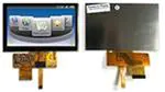


 工商网监
湘ICP备2023018690号
工商网监
湘ICP备2023018690号
