NJM2930
LOW DROP OUT VOLTAGE REGULATOR
■ GENERAL DESCRIPTION
The NJM2930 3-terminal positive voltage regulator features an
ability to source 150mA of output current (100mA: L-Type) with an
input-output differential of 0.6V or less. Efficient use of low input
voltages obtained, for example, from an automotive battery during
cold crank conditions, allows 5V circuitry to be properly powered with
supply voltages as low as 5.6V.
Familiar regulator features such as current limit and thermal
overload protection are also provided.
■ PACKAGE OUTLINE
1. Input
2. GND
3. Output
NJM2930F
1. Output
2. GND
3. Input
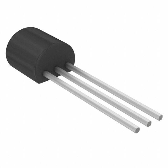
NJM2930L
■ FEATURES
• Operating Voltage
• Input-Output differential less 0.6V
• Output Current in Excess of 150mA
• 40V Load Dump Protection
• Internal Short Circuit Current Limit
• Internal Thermal Overload Protection
• Package Outline
TO-220F, TO-92
• Bipolar Technology
■ EQUIVALENT CIRCUIT
Ver.2003-07-18
-1-
�NJM2930
■ ABSOLUTE MAXIMUM RATINGS
(Ta = 25°C)
PARAMETER
SYMBOL
RATINGS
UNIT
Operating Input Voltage Range
VIN
26
V
Input Overvoltage Protection
VPR
40
V
Input Reverse Voltage
VINR1(100ms)
-12
V
Input Reverse Voltage
VINR2(DC)
-6
V
Maximum Output Current
IOM
(TO-92) 100
(TO-220F) 150
mA
mA
Power Dissipation
PD
(TO-92) 500
(TO-220F) 7.5 (Note)
mW
W
Operating Temperature Range
Topr
-30 to 75
ºC
Storage Temperature Range
Tstg
-40 to 125
ºC
(note) Case Temperature : Tcase ≤ 75°C, Thermal Resistance : θjc = 5°C/W TYP.
■ ELECTRICAL CHARACTERISTICS
(All characteristics except noise voltage and ripple rejection ratio are measured using pulse techniques.)
NJM2930F05 (VIN = 14V, C2 = 10µF, Tj = 25°C)
PARAMETER
Output Voltage
Line Regulation
SYMBOL
VO
∆VO - VI
Load Regulation
Quiescent Current
∆VO - VI
∆VO - IO
IQ1
Dropout Voltage
IQ2
∆VI - O
Output Noise Voltage
VNO
Ripple Rejection
RR
TEST CONDITION
6V ≤ VIN ≤ 26V, 5mA ≤ IO ≤ 100mA
MIN.
4.5
-
TYP.
5
7
MAX.
5.5
25
UNIT
V
mV
IO=10mA
-
30
14
4
80
50
7
mV
mV
mA
IO=150mA
-
30
40
mA
IO=150mA
-
0.3
0.6
V
10Hz to 100kHz, IO= 150mA
-
100
-
µV
f=120Hz, IO= 150mA
-
60
-
dB
MIN.
4.5
-
TYP.
5
7
MAX.
5.5
25
UNIT
V
mV
IO=10mA
-
30
14
4
80
50
7
mV
mV
mA
-
25
40
mA
9V ≤ VIN ≤ 16V, IO=5mA
6V ≤ VIN ≤ 26V, IO=5mA
5mA ≤ IO ≤ 150mA
NJM2930L 05 (VIN = 14V, C2 = 10µF, Tj = 25°C)
PARAMETER
Output Voltage
Line Regulation
SYMBOL
VO
∆VO - VI
Load Regulation
Quiescent Current
∆VO - VI
∆VO - IO
IQ1
IO=100mA
Dropout Voltage
IQ2
∆VI - O
IO=100mA
-
0.25
0.6
V
Output Noise Voltage
VNO
10Hz to 100kHz, IO= 40mA, VIN=10V
-
100
-
µV
Ripple Rejection
RR
f=120Hz, IO= 40mA, VIN
-
60
-
dB
-2-
TEST CONDITION
6V ≤ VIN ≤ 26V, 5mA ≤ IO ≤ 100mA
9V ≤ VIN ≤ 16V, IO=5mA
6V ≤ VIN ≤ 26V, IO=5mA
5mA ≤ IO ≤ 100mA
Ver.2003-07-18
�NJM2930
NJM2930F08 (VIN = 14V, C2 = 10µF, Tj = 25°C)
PARAMETER
Output Voltage
Line Regulation
SYMBOL
VO
∆VO - VI
Load Regulation
Quiescent Current
∆VO - VI
∆VO - IO
IQ1
Dropout Voltage
IQ2
∆VI - O
Output Noise Voltage
VNO
Ripple Rejection
RR
TEST CONDITION
9.4V ≤ VIN ≤ 26V, 5mA ≤ IO ≤ 150mA
MIN.
7.2
-
TYP.
8
12
MAX.
8.8
50
UNIT
V
mV
IO=10mA
-
50
25
4
100
50
7
mV
mV
mA
IO=150mA
-
30
40
mA
IO=150mA
-
0.3
0.6
V
10Hz to 100kHz, IO= 150mA
-
140
-
µV
f=120Hz, IO= 150mA
-
57
-
dB
MIN.
7.2
-
TYP.
8
12
MAX.
8.8
50
UNIT
V
mV
IO=10mA
-
50
25
4
100
50
7
mV
mV
mA
9.4V ≤ VIN ≤ 16V, IO=5mA
9.4V ≤ VIN ≤ 26V, IO=5mA
5mA ≤ IO ≤ 150mA
NJM2930L 08 (VIN = 14V, C2 = 10µF, Tj = 25°C)
PARAMETER
Output Voltage
Line Regulation
SYMBOL
VO
∆VO - VI
TEST CONDITION
9.4V ≤ VIN ≤ 26V, 5mA ≤ IO ≤ 100mA
Load Regulation
Quiescent Current
∆VO - VI
∆VO - IO
IQ1
IQ2
∆VI - O
IO=100mA
-
25
40
mA
Dropout Voltage
IO=100mA
-
0.25
0.6
V
Output Noise Voltage
VNO
10Hz to 100kHz, IO= 40mA
-
140
-
µV
Ripple Rejection
RR
f=120Hz, IO= 40mA
-
57
-
dB
MIN.
7.65
-
TYP.
8.5
12
MAX.
9.35
50
UNIT
V
mV
50
25
4
100
50
7
mV
mV
mA
9.4V ≤ VIN ≤ 16V, IO=5mA
9.4V ≤ VIN ≤ 26V, IO=5mA
5mA ≤ IO ≤ 150mA
NJM2930F85 (VIN = 14V, C2 = 10µF, Tj = 25°C)
PARAMETER
Output Voltage
Line Regulation
SYMBOL
VO
∆VO - VI
TEST CONDITION
9.95V ≤ VIN ≤ 26V, 5mA ≤ IO ≤ 150mA
Load Regulation
Quiescent Current
∆VO - VI
∆VO - IO
IQ1
IO=10mA
-
IO=150mA
-
30
40
mA
Dropout Voltage
IQ2
∆VI - O
IO=150mA
-
0.3
0.6
V
Output Noise Voltage
VNO
10Hz to 100kHz, IO= 150mA
-
150
-
µV
Ripple Rejection
RR
f=120Hz, IO= 150mA
-
56
-
dB
MIN.
7.65
-
TYP.
8.5
12
MAX.
9.35
50
UNIT
V
mV
50
25
4
100
50
7
mV
mV
mA
mA
9.95V ≤ VIN ≤ 16V, IO=5mA
9.95V ≤ VIN ≤ 26V, IO=5mA
5mA ≤ IO ≤ 150mA
NJM2930L 85 (VIN = 14V, C2 = 10µF, Tj = 25°C)
PARAMETER
Output Voltage
Line Regulation
SYMBOL
VO
∆VO - VI
Load Regulation
Quiescent Current
∆VO - VI
∆VO - IO
IQ1
IO=10mA
-
IO=100mA
-
25
40
Dropout Voltage
IQ2
∆VI - O
IO=100mA
-
0.25
0.6
V
Output Noise Voltage
VNO
10Hz to 100kHz, IO= 40mA
-
150
-
µV
Ripple Rejection
RR
f=120Hz, IO= 40mA
-
56
-
dB
Ver.2003-07-18
TEST CONDITION
9.95V ≤ VIN ≤ 26V, 5mA ≤ IO ≤ 100mA
9.95V ≤ VIN ≤ 16V, IO=5mA
9.4V ≤ VIN ≤ 26V, IO=5mA
5mA ≤ IO ≤ 100mA
-3-
�NJM2930
■ STANDARD APPLICATION EXAMPLES
* This NJM2930 is required when the mounting position is separated from the power filter.
** Use an aluminum electrolytic capacitor or a tantalum capacitor as C2. The temperature guarantee range of
capacitors should be down to -30°C. A capacity value of 10µF is a minimum requirement for improving the stability
and transient response. Mount it at a position as close to the leads as possible.
*** When application on automobile car operation, the minus pulse might
be input on IC. In this case, however, the pulse might trigger to latch up.
If it were that, this kind of latching up might be continued, the IC would
burn up into defective in many cases. It is advisable to apply D1, D2
as described in the drawing, in order to prevent from making any
troubles. It is important to make devices D1, D2 against VIN to be able
to stand for brake down voltage, current volume, and then less volume
for Vf.
■ POWER DISSIPATION VS. AMBIENT TEMPERATURE
NJM2930 (TO-220F)
-4-
NJM2930L (TO-92)
Ver.2003-07-18
�NJM2930
■ TYPICAL CHARACTERISTICS
NJM2930F05/L05 Output Voltage
NJM2930F05/L05 Icc-VIN
NJM2939F05/L05 Thermal Shutdown
NJM2930L05 Output Current
vs. Quiescent Current
Ver.2003-07-18
NJM2930F05/L05 Load Characteristics
NJM2930F05 Output Current
vs. Quiescent Current
-5-
�NJM2930
■ TYPICAL CHARACTERISTICS
NJM2930F05/L05 Ripple Rejection
vs. Frequency
NJM2930L05 Dropout Voltage
NJM2930F05/L05 Output Voltage
NJM2930F05 Dropout Voltage
NJM2930F05 Dropout Voltage
vs. Output Current
[CAUTION]
The specifications on this databook are only
given for information , without any guarantee
as regards either mistakes or omissions. The
application circuits in this databook are
described only to show representative usages
of the product and not intended for the
guarantee or permission of any right including
the industrial rights.
-6-
Ver.2003-07-18
�


 工商网监
湘ICP备2023018690号
工商网监
湘ICP备2023018690号
