NJM79L00
3-TERMINAL NEGATIVE VOLTAGE REGULATOR
■ GENERAL DESCRIPTION The NJM79L00 series of 3-Terminal Negative Voltage Regulators is constructed using the New JRC Planar epitaxial process. These regulators employ internal current-limiting, and thermal-shutdown, making them essentially indestructible. If adequate heat sinking is provided, they can deliver up to 100mA output current. They are intended as fixed voltage regulators in a wide range of applications including local or on-card regulation for elimination of noise and distribution problems associated with single-point regulation. In addition, they can be used with power pass elements to make high-current voltage regulators. The NJM79L00 used as a Zener diode/resistor combination replacement, offers an effective output impedance improvement of typically two orders of magnitude, along with lower quiescent current and lower noise. ■ PACKAGE OUTLINE
NJM79L00A
NJM79L00UA
1. COMMON 2. IN 3. OUT
■ FEATURES • Internal Short Circuit Current Limit • Internal Thermal Overload Protection • Excellent Ripple Rejection • Guarantee'd 100mA Output Current • Package Outline TO-92, SOT-89 • Bipolar Technology
■ EQUIVALENT CIRCUIT
Ver.2003-07-18
-1-
�NJM79L00
■ ABSOLUTE MAXIMUM RATINGS
PARAMETER Input Voltage Operating Temperature Range Storage Temperature Range Power Dissipation SYMBOL VIN Topr Tstg PD RATINGS (79L03A to 79L09A) - 30 (79L12A to 79L15A) - 35 (79L18A to 79L24A) - 40 -40 to +85 -40 to +125 (TO92) 500 (SOT89) 350 UNIT V V V ºC ºC mW mW
■ ELECTRICAL CHARACTERISTICS (CIN=0.33µF, CO=1.0µF, Tj=25ºC) Measurement is to be conducted in pulse testing.
PARAMETER SYMBOL TEST CONDITION MIN. TYP. MAX. UNIT
NJM79L03A
Output Voltage Line Regulation Load Regulation Quiescent Current Ripple Rejection Output Noise Voltage VO ∆VO - VIN ∆VO - IO IQ RR VNO VIN=-10V, I0=40mA VIN=-7 to -20V, IO=40mA VIN=-10V, IO=1 to 100mA VIN=-10V, IO=0mA VIN=-8 to -18V, IO=40mA, ein=1VP-P, f=120Hz VIN=-10V, BW=10Hz to 100kHz, IO=40mA -2.88 45 -3.0 10 4 3.5 72 70 -3.12 60 72 6.0 V mV mV mA dB µV
NJM79L05A
Output Voltage Line Regulation Load Regulation Quiescent Current Ripple Rejection Output Noise Voltage VO ∆VO - VIN ∆VO - IO IQ RR VNO VIN=-10V, I0=40mA VIN=-7 to -20V, IO=40mA VIN=-10V, IO=1 to 100mA VIN=-10V, IO=0mA VIN=-8 to -18V, IO=40mA, ein=1VP-P, f=120Hz VIN=-10V, BW=10Hz to 100kHz, IO=40mA -4.8 41 -5.0 15 7 3.5 71 120 -5.2 150 60 6.0 V mV mV mA dB µV
-2-
Ver.2003-07-18
�NJM79L00
■ ELECTRICAL CHARACTERISTICS (CIN=0.33µF, CO=1.0µF, Tj=25ºC) Measurement is to be conducted in pulse testing.
PARAMETER SYMBOL TEST CONDITION MIN. TYP. MAX. UNIT
NJM79L06A
Output Voltage Line Regulation Load Regulation Quiescent Current Ripple Rejection Output Noise Voltage VO ∆VO - VIN ∆VO - IO IQ RR VNO VIN=-12V, I0=40mA VIN=-8.5 to -20V, IO=40mA VIN=-12V, IO=1 to 100mA VIN=-12V, IO=0mA VIN=-9 to -19V, IO=40mA, ein=1VP-P, f=120Hz VIN=-12V, BW=10Hz to 100kHz, IO=40mA -5.76 40 -6.0 18 8 3.5 68 140 -6.24 150 70 6.0 V mV mV mA dB µV
NJM79L08A
Output Voltage Line Regulation Load Regulation Quiescent Current Ripple Rejection Output Noise Voltage VO ∆VO - VIN ∆VO - IO IQ RR VNO VIN=-14V, I0=40mA VIN=-10.5 to -23V, IO=40mA VIN=-14V, IO=1 to 100mA VIN=-14V, IO=0mA VIN=-11 to -21V, IO=40mA, ein=1VP-P, f=120Hz VIN=-14V, BW=10Hz to 100kHz, IO=40mA -7.68 39 -8.0 24 10 3.5 68 190 -8.32 175 80 6.0 V mV mV mA dB µV
NJM79L09A
Output Voltage Line Regulation Load Regulation Quiescent Current Ripple Rejection Output Noise Voltage VO ∆VO - VIN ∆VO - IO IQ RR VNO VIN=-15V, I0=40mA VIN=-11.5 to -24V, IO=40mA VIN=-15V, IO=1 to 100mA VIN=-15V, IO=0mA VIN=-12 to -22V, IO=40mA, ein=1VP-P, f=120Hz VIN=-15V, BW=10Hz to 100kHz, IO=40mA -8.64 38 -9.0 27 12 3.5 67 210 -9.36 200 90 6.0 V mV mV mA dB µV
NJM79L12A
Output Voltage Line Regulation Load Regulation Quiescent Current Ripple Rejection Output Noise Voltage VO ∆VO - VIN ∆VO - IO IQ RR VNO VIN=-19V, I0=40mA VIN=-14.5 to -27V, IO=40mA VIN=-19V, IO=1 to 100mA VIN=-19V, IO=0mA VIN=-15 to -25V, IO=40mA, ein=1VP-P, f=120Hz VIN=-19V, BW=10Hz to 100kHz, IO=40mA -11.5 37 -12.0 36 16 3.5 64 210 -12.5 250 100 6.5 V mV mV mA dB µV
Ver.2003-07-18
-3-
�NJM79L00
■ ELECTRICAL CHARACTERISTICS (CIN=0.33µF, CO=1.0µF, Tj=25ºC) Measurement is to be conducted in pulse testing.
PARAMETER SYMBOL TEST CONDITION MIN. TYP. MAX. UNIT
NJM79L15A
Output Voltage Line Regulation Load Regulation Quiescent Current Ripple Rejection Output Noise Voltage VO ∆VO - VIN ∆VO - IO IQ RR VNO VIN=-23V, I0=40mA VIN=-17.5 to -30V, IO=40mA VIN=-23V, IO=1 to 100mA VIN=-23V, IO=0mA VIN=-18.5 to -28.5V, IO=40mA, ein=1VP-P, f=120Hz VIN=-23V, BW=10Hz to 100kHz, IO=40mA -14.4 34 -15.0 45 20 3.5 63 340 -15.6 300 150 6.5 V mV mV mA dB µV
NJM79L18A
Output Voltage Line Regulation Load Regulation Quiescent Current Ripple Rejection Output Noise Voltage VO ∆VO - VIN ∆VO - IO IQ RR VNO VIN=-27V, I0=40mA VIN=-20.7 to -33V, IO=40mA VIN=-27V, IO=1 to 100mA VIN=-27V, IO=0mA VIN=-23 to -33V, IO=40mA, ein=1VP-P, f=120Hz VIN=-27V, BW=10Hz to 100kHz, IO=40mA -17.3 33 -18.0 54 23 3.5 60 410 -18.7 325 170 6.5 V mV mV mA dB µV
NJM79L24A
Output Voltage Line Regulation Load Regulation Quiescent Current Ripple Rejection Output Noise Voltage VO ∆VO - VIN ∆VO - IO IQ RR VNO VIN=-33V, I0=40mA VIN=-27 to -38V, IO=40mA VIN=-33V, IO=1 to 100mA VIN=-33V, IO=0mA VIN=-29 to -35V, IO=40mA, ein=1VP-P, f=120Hz VIN=-33V, BW=10Hz to 100kHz, IO=40mA -23.0 31 -24.0 72 30 3.5 55 550 -25.0 350 200 6.5 V mV mV mA dB µV
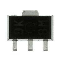
■ SOT-89 MARK
(1)
(2) B C E G H K L M P
(1) 9: Negative Output (2) Vo Rank (3) The end of A. D. (4) Production Month Oct. ···X Nov. ···Y Dec. ···Z
NJM79L03UA NJM79L05UA NJM79L06UA NJM79L08UA NJM79L09UA NJM79L12UA NJM79L15UA NJM79L18UA NJM79L24UA
9 9 9 9 9 9 9 9 9
-4-
Ver.2003-07-18
�NJM79L00
■ TEST CIRCUIT 1. Output Voltage, Output Current, Line Regulation, Road Regulation, Quiescent Current, Output Noise Voltage
2. Ripple Rejection
■ POWER DISSIPATION VS. AMBIENT TEMPERATURE
Ver.2003-07-18
-5-
�NJM79L00
■ TYPICAL CHARACTERISTICS NJM79L00 Input Voltage vs. Output Voltage
NJM79L05/15/24 Load Characteristics
NJM79L00 Series Short Circuit Current
NJM79L05/12/24 Output Voltage vs. Junction Temperature
NJM79L05/15/24 Ripple Rejection vs. Frequency
Quiescent Current vs. Input Voltage
-6-
Ver.2003-07-18
�NJM79L00
■ TYPICAL CHARACTERISTICS
NJM79L05 Dropout Characteristics
NJM79L08 Dropout Characteristics
NJM79L05 Output Voltage vs. Temperature
NJM79L08 Output Voltage vs. Temperature
[CAUTION] The specifications on this databook are only given for information , without any guarantee as regards either mistakes or omissions. The application circuits in this databook are described only to show representative usages of the product and not intended for the guarantee or permission of any right including the industrial rights.
Ver.2003-07-18
-7-
�


 工商网监
湘ICP备2023018690号
工商网监
湘ICP备2023018690号
