NTE2388
MOSFET
N−Channel Enhancement Mode,
High Speed Switch
Description:
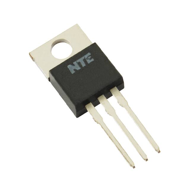
The NTE2388 is an N−Channel Enhancement Mode Power MOS Field Effect Transistor in a TO220
type package designed for low voltage, high speed power switching applications such as switching
regulators, converters, solenoid, and relay drivers.
D
Features:
D Silicon Gate for Fast Switching Speeds
D Low rDS(on) to Minimize On−Losses.
Specified at Elevated Temperatures.
D Rugged − SOA is Power Dissipation Limited
D Source−to−Drain Diode Characterized for Use With Inductive Loads
G
S
Absolute Maximum Ratings:
Drain−Source Voltage, VDSS . . . . . . . . . . . . . . . . . . . . . . . . . . . . . . . . . . . . . . . . . . . . . . . . . . . . . . . . 200V
Drain−Gate Voltage (RGS = 20k+ ), VDGR . . . . . . . . . . . . . . . . . . . . . . . . . . . . . . . . . . . . . . . . . . . . . 200V
Gate−Source Voltage, VGS . . . . . . . . . . . . . . . . . . . . . . . . . . . . . . . . . . . . . . . . . . . . . . . . . . . . . . . . . +20V
Drain Current, ID
Continuous
TC = +255C . . . . . . . . . . . . . . . . . . . . . . . . . . . . . . . . . . . . . . . . . . . . . . . . . . . . . . . . . . . . . . . 18A
TC = +1005C . . . . . . . . . . . . . . . . . . . . . . . . . . . . . . . . . . . . . . . . . . . . . . . . . . . . . . . . . . . . . . 11A
Peak
TC = +255C . . . . . . . . . . . . . . . . . . . . . . . . . . . . . . . . . . . . . . . . . . . . . . . . . . . . . . . . . . . . . . . 72A
Total Power Dissipation (TC = +255C), PD . . . . . . . . . . . . . . . . . . . . . . . . . . . . . . . . . . . . . . . . . . . 125W
Derate Above 255C . . . . . . . . . . . . . . . . . . . . . . . . . . . . . . . . . . . . . . . . . . . . . . . . . . . . . . . . . 1W/5C
Maximum Operating Junction Temperature Range, TJ . . . . . . . . . . . . . . . . . . . . . . . . . −555 to +1505C
Storage Temperature Range, Tstg . . . . . . . . . . . . . . . . . . . . . . . . . . . . . . . . . . . . . . . . . . −555 to +1505C
Maximum Thermal Resistance, Junction−to−Case, RthJC . . . . . . . . . . . . . . . . . . . . . . . . . . . . . . 15C/W
Maximum Thermal Resistance, Junction−to−Ambient, RthJA . . . . . . . . . . . . . . . . . . . . . . . . 62.55C/W
Maximum Lead Temperature (During soldering, 1/8” from case for 5sec), TL . . . . . . . . . . . . +3005C
Rev. 10−13
�Electrical Characteristics: (TC = +255C unless otherwise specified)
Parameter
Symbol
Test Conditions
Min
Typ
Max
Unit
200
−
−
V
VGS = 0, VDS = Max Rating
−
−
200
.A
VGS = 0, VDS = 160V,
TC = +1255C
−
−
1000
.A
OFF Characteristics
Drain−Source Breakdown Voltage
Zero−Gate Voltage Drain Current
V(BR)DSS ID = 250.A, VGS = 0
IDSS
Gate−Body Leakage Current, Forward
IGSSF
VDS = 0, VGSF = 20V
−
−
100
nA
Gate−Body Leakage Current, Reverse
IGSSR
VDS = 0, VGSR = 20V
−
−
100
nA
Gate Threshold Voltage
VGS(th)
VDS = VGS, ID = 250.A
2
−
4
V
Static Drain−Source On Resistance
RDS(on)
VGS = 10V, ID = 10A
−
−
0.18
+
VGS = 10V, VDS . 3.2V
18
−
−
A
gfs
VDS . 3.2V, ID = 10A
6
−
−
mhos
Input Capactiance
Ciss
−
−
1600
pf
Output Capacitance
Coss
VDS = 25V, VGS = 0,
f = 1MHz
−
−
750
pf
Reverse Transfer Capactiance
Crss
−
−
300
pf
−
−
30
ns
−
−
60
ns
td(off)
−
−
80
ns
tf
−
−
60
ns
−
38
60
nC
−
16
−
nC
−
22
−
nC
−
1.8
2.0
V
ON Characteristics (Note 1)
On−State Drain Current
Forward Transconductance
ID(on)
Dynamic Characteristics
Switching Characteristics (Note 1)
Turn−On Time
Rise Time
Turn−Off Delay Time
Fall Time
td(on)
tr
Total Gate Charge
Qg
Gate−Source Charge
Qgs
Gate−Drain Charge
Qgd
VDD [ 75V, ID = 10APEAK,
Rg = 4.7+
VDS = 160V, VGS = 10V,
ID = Rated ID
Source Drain Diode Characteristics (Note 1)
Forward ON Voltage
VSD
Forward Turn−On Time
ton
Reverse Recovery Time
trr
IS = Rated ID, VGS = 0
Limited by stray inductance
−
450
−
ns
Measured from the contact
screw on tab to center of die
−
3.5
−
nH
Measured from the drain lead
0.25” from package to center
of die
−
4.5
−
nH
Measured from the source
lead 0.25” from package to
source bond pad
−
7.5
−
nH
Internal Package Inductance
Internal Drain Inductance
Internal Source Inductance
Ld
Ls
Note 1. Pulse test: Pulse width 3 300.s, Duty cycle 3 2%.
�.420 (10.67)
Max
.110 (2.79)
.147 (3.75) Dia Max
.500
(12.7)
Max
.250 (6.35)
Max
.500
(12.7)
Min
.070 (1.78) Max
Gate
.100 (2.54)
Source
Drain/Tab
�
很抱歉,暂时无法提供与“NTE2388”相匹配的价格&库存,您可以联系我们找货
免费人工找货- 国内价格
- 1+146.44345
- 3+113.12099
- 7+81.81542
- 25+54.98207


 工商网监
湘ICP备2023018690号
工商网监
湘ICP备2023018690号

