NTE74HC153
Integrated Circuit
TTL − High Speed CMOS,
Dual 4−Line−to−1−Line Data Selector/ Multiplexer
Description:
The NTE74HC153 is a high speed CMOS dual multiplexer in a 16−Lead DIP type package fabricated
with silicon−gate C2MOS technology. Along with high noise immunity and low power dissipation of
standard CMOS integrated circuits, it possesses the ability to drive 15 LS−TTL loads. Each data input
(1C0 − 1C3, 2C0 − 2C3) of the NTE74HC153 is selected by the two address inputs A and B. Separate
strobe inputs (1G, 2G) are provided for each of the two four−line selectors. The strobe input (G) can
be used to inhibit the data output; the output of the NTE74HC153 is fixed in the low level, while the
strobe input is held low.
The 74HC logic family is functionally, as well as pinout compatible, with the standard 74LS logic family.
All inputs are protected from damage due to static discharge by internal diode clamps to VCC and
GND.
Features:
D Wide Operating Supply Voltage Range: 2V to 6V
D Outputs Can Drive up to 15 LS−TTL Loads
D Low Power Consumption: 80μA (max)
D Typical Propagation Delay: 9ns
D Low Input Current: 1μA (max)
D Permit Multiplexing from n Lines to One Line
D Perform Parallel−to−Serial Conversion
D Strobe (Enable) Line Provided for cascading (N Lines to n Lines)
Absolute Maximum Ratings: (Note 1, Note 2)
Supply Voltage Range, VCC . . . . . . . . . . . . . . . . . . . . . . . . . . . . . . . . . . . . . . . . . . . . . . . . −0.5 to +7.0V
Clamp Diode Current (Note 3), IIK, IOK . . . . . . . . . . . . . . . . . . . . . . . . . . . . . . . . . . . . . . . . . . . . . ±20mA
DC Output Current (Per Pin), IOUT . . . . . . . . . . . . . . . . . . . . . . . . . . . . . . . . . . . . . . . . . . . . . . . . . ±35mA
DC VCC or GND Current (Per Pin), ICC . . . . . . . . . . . . . . . . . . . . . . . . . . . . . . . . . . . . . . . . . . . . . ±70mA
Storage Temperature Range, Tstg . . . . . . . . . . . . . . . . . . . . . . . . . . . . . . . . . . . . . . . . −65°C to +150°C
Thermal Impedance, Junction−to−Ambient, RthJA . . . . . . . . . . . . . . . . . . . . . . . . . . . . . . . . . . . 73°C/W
Note 1. Absolute Maximum Ratings are those values beyond which damage to the device may occur.
Note 2. Unless otherwise specified, all voltages are referenced to GND.
Note 3. Th input and output voltage ratings may be exceeded if the input and output current ratings
are observed.
�Recommended Operating Conditions: (Note 4)
Parameter
Symbol
Min
Typ
Max
Unit
VCC
2.0
5.0
6.0
V
VIN, VOUT
0
−
VCC
V
Operating Temperature Range
TA
−40
−
+85
°C
High−Level Input Voltage
VCC = 2.0V
VIH
1.5
−
−
V
VCC = 4.5V
3.15
−
−
V
VCC = 6.0V
4.2
−
−
V
−
−
0.5
V
VCC = 4.5V
−
−
1.35
V
VCC = 6.0V
−
−
1.8
V
Supply Voltage
DC Input or Output Voltage
Low−Level Input Voltage
VCC = 2.0V
VIH
Note 4. All unused inputs of the device must be held at VCC or GND to ensure proper device operation.
Electrical Characteristics:
TA = +25°C
Parameter
High Level Output Voltage
Symbol
VOH
Low Level Output Voltage
VCC
Min
Typ
Max
Min
Max
Unit
2.0
1.9
1.998
−
1.9
−
V
4.5
4.4
4.499
−
4.4
−
V
6.0
5.9
5.999
−
5.9
−
V
IOH = −6mA
4.5
3.98
4.3
−
3.84
−
V
IOH = −7.8mA
6.0
5.48
5.8
−
5.34
−
V
2.0
−
0.002
0.1
−
0.1
V
4.5
−
0.001
0.1
−
0.1
V
0.001
0.1
−
0.1
V
Test Conditions
VIN = VIH or VIL, IOH = −20μA
VIN = VIH
or VIL
VOL
VIN = VIH or VIL, IOL = 20μA
6.0
VIN = VIH
or VIL
TA = −40° to +85°C
IOL = 6mA
4.5
−
0.17
0.26
−
0.33
V
IOL = 7.8mA
6.0
−
0.15
0.26
−
0.33
V
Input Current
IIN
VIN = VCC or GND
6.0
−
±0.1
±100
±1.0
±1000
nA
Quiescent Supply Current
ICC
VIN = VCC or GND, IOUT = 0μA
6.0
−
−
8
−
80
μA
Input Capacitance
CI
−
3
10
−
10
pF
Switching Characteristics: (tr = tf = 6ns, Note 5)
TA = +25°C
Parameter
Propagation Delay Time
A or B to Y
Symbol
tpd
Test Conditions
CL = 50pF
CL = 150pF
TA = −40° to +85°C
VCC
Min
Typ
Max
Min
Max
Unit
2.0
−
90
150
−
190
ns
4.5
−
21
30
−
38
ns
6.0
−
17
26
−
32
ns
2.0
−
105
235
−
295
ns
4.5
−
27
47
−
59
ns
6.0
−
21
41
−
51
ns
�Switching Characteristics (Cont’d): (tr = tf = 6ns, Note 5)
TA = +25°C
Parameter
Symbol
Propagation Delay Time
Data (Any C) to Y
tpd
Test Conditions
CL = 50pF
CL = 150pF
Propagation Delay Time
G to Y
tpd
CL = 50pF
CL = 150pF
Output Rise and Fall Time
tt
CL = 50pF
CL = 150pF
Power Dissipation Capacitance,
Per Multiplexer
CPD
No Load
TA = −40° to +85°C
VCC
Min
Typ
Max
Min
Max
Unit
2.0
−
73
126
−
158
ns
4.5
−
17
28
−
35
ns
6.0
−
14
23
−
29
ns
2.0
−
93
220
−
274
ns
4.5
−
23
44
−
55
ns
6.0
−
19
38
−
48
ns
2.0
−
38
95
−
125
ns
4.5
−
11
19
−
24
ns
6.0
−
9
16
−
20
ns
2.0
−
60
185
−
230
ns
4.5
−
17
37
−
46
ns
6.0
−
14
32
−
40
ns
2.0
−
20
60
−
75
ns
4.5
−
8
12
−
15
ns
6.0
−
6
10
−
13
ns
2.0
−
45
210
−
265
ns
4.5
−
17
42
−
53
ns
6.0
−
13
36
−
45
ns
−
−
40
−
−
−
pF
Note 5. tPLH and tPHL are the same as tpd.
Truth Table:
Select *
A
B
X
X
L
L
L
L
L
H
L
H
H
L
H
L
H
H
H
H
C0
X
L
H
X
X
X
X
X
X
Inputs
Data
C1
C2
X
X
X
X
X
X
L
X
H
X
X
L
X
H
X
X
X
X
Output
C3
X
X
X
X
X
X
X
L
H
G
H
L
L
L
L
L
L
L
L
* Select inputs A and B are common to both sections.
Y
L
L
H
L
H
L
H
L
H
�Pin Connection Diagram
Strobe 1G 1
16 VCC
Select B 2
Data Input 1C 3 3
15 Strobe 2G
14 Select A
Data Input 1C 2 4
13 Data Input 2C 3
Data Input 1C 1 5
12 Data input 2C 2
Data Input 1C 0 6
11 Data Input 2C 1
Output 1Y 7
10 Data Input 2C 0
GND 8
9 Output 2Y
16
9
1
8
.870 (22.0) Max
.260 (6.6)
Max
.200
(5.08)
Max
.100 (2.54)
.700 (17.78)
.099 (2.5) Min
�
很抱歉,暂时无法提供与“NTE74HC153”相匹配的价格&库存,您可以联系我们找货
免费人工找货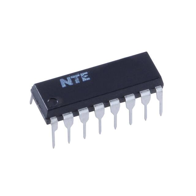


 工商网监
湘ICP备2023018690号
工商网监
湘ICP备2023018690号
