INTEGRATED CIRCUITS
74ABT16374B
16-bit D-type flip-flop;
positive-edge trigger (3-State)
Product data
Supersedes data of 2004 Mar 01
�����
�����
����
�
2004 Mar 08
�Philips Semiconductors
Product data
16-bit D-type flip-flop; positive-edge trigger
(3-State)
DESCRIPTION
74ABT16374B
FEATURES
• Two 8-bit positive edge triggered registers
• Live insertion/extraction permitted
• Power-up 3-State
• Power-up reset
• Multiple VCC and GND pins minimize switching noise
• 3-State output buffers
• Output capability: +64 mA/–32 mA
• Latch-up protection exceeds 500mA per JEDEC Std 17
• ESD protection exceeds 2000 V per MIL STD 883 Method 3015
The 74ABT16374B high-performance BiCMOS device combines
low static and dynamic power dissipation with high speed and high
output drive.
The 74ABT16374B has two 8-bit, edge triggered registers, with each
register coupled to eight 3-State output buffers. The two sections of
each register are controlled independently by the clock (nCP) and
Output Enable (nOE) control gates.
Each register is fully edge triggered. The state of each D input, one
set-up time before the LOW-to-HIGH clock transition, is transferred
to the corresponding flip-flop’s Q output.
The 3-State output buffers are designed to drive heavily loaded
3-State buses, MOS memories, or MOS microprocessors. Each
active-LOW Output Enable (nOE) controls all eight 3-State buffers
for its register independent of the clock operation.
and 200 V per Machine Model
When nOE is LOW, the stored data appears at the outputs for that
register. When nOE is HIGH, the outputs for that register are in the
high-impedance “OFF” state, which means they will neither drive nor
load the bus.
QUICK REFERENCE DATA
SYMBOL
CONDITIONS
Tamb = 25 °C; GND = 0 V
PARAMETER
tPLH
tPHL
Propagation delay
nCP to nQx
CL = 50 pF; VCC = 5 V
CIN
Input capacitance
VI = 0 V or VCC
Output capacitance
VO = 0V or VCC; 3-State
COUT
ICCZ
ICCL
Outputs disabled; VCC = 5.5 V
Quiescent supply current
TYPICAL
UNIT
2.6
2.2
ns
4
pF
7
pF
500
µA
8
mA
Outputs LOW; VCC = 5.5 V
ORDERING INFORMATION
Tamb = –40 °C to +85 °C
Type number
Package
Name
Description
Version
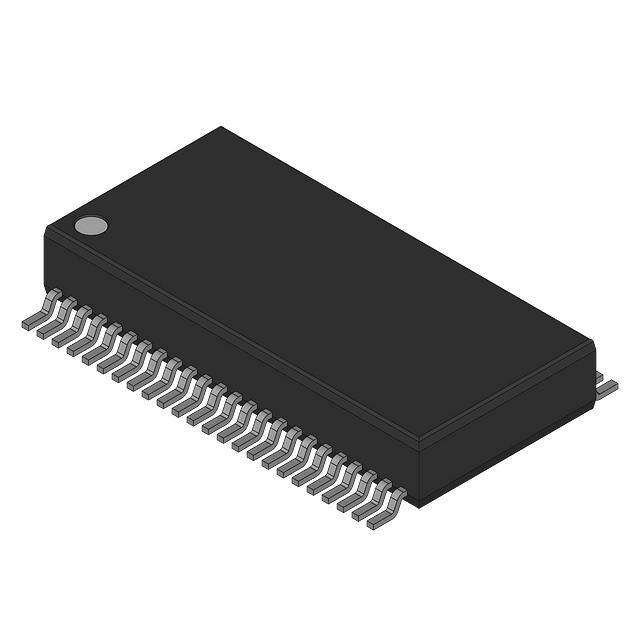
74ABT16374BB
QFP52
plastic quad flat package; 52 leads (lead length 1.6 mm); body 10 × 10 × 2.0 mm
SOT379-1
74ABT16374BDGG
TSSOP48
plastic thin shrink small outline package; 48 leads; body width 6.1 mm
SOT362-1
74ABT16374BDL
SSOP48
plastic shrink small outline package; 48 leads; body width 7.5 mm
SOT370-1
2004 Mar 08
2
�Philips Semiconductors
Product data
16-bit D-type flip-flop; positive-edge trigger
(3-State)
74ABT16374B
PIN CONFIGURATION
TSSOP48 and SSOP48 pinning
QFP52 pinning
1
39
VCC
44
1D2
1Q4
2
38
1D4
1Q3
6
43
1D3
1Q5
3
37
1D5
VCC
7
42
VCC
GND
4
36
GND
1Q4
8
41
1D4
1Q6
5
35
1D6
1Q5
9
40
1D5
1Q7
6
34
1D7
GND
10
39
GND
GND
7
33
GND
1Q6
11
38
1D6
2Q0
8
32
2D0
1Q7
12
37
1D7
2Q1
9
31
2D1
2Q0
13
36
2D0
GND 10
30
GND
2Q1
14
35
2D1
2Q2 11
29
2D2
GND
15
34
GND
2Q3 12
28
2D3
2Q2
16
33
2D2
VCC 13
27
VCC
2Q3
17
32
2D3
VCC
18
31
VCC
2Q4
19
30
2D4
2Q5
20
29
2D5
GND
21
28
GND
2Q6
22
27
2D6
2Q7
23
26
2D7
2OE
24
25
2CP
2D4 26
2D5 25
GND 24
2D6 23
2D7 22
2CP 21
GND 20
2OE 19
2Q7 18
2Q6 17
GND 16
2Q4 14
2Q5 15
74ABT16374BB
QFP52
SW02219
SA00326
PIN DESCRIPTION
PIN NUMBER
SYMBOL
FUNCTION
TSSOP and SSOP
QFP52
47, 46, 44, 43, 41, 40, 38, 37
36, 35, 33, 32, 30, 29, 27, 26
44, 43, 41, 40, 38, 37, 35, 34
32, 31, 29, 28, 26, 25, 23, 22
1D0 – 1D7
2D0 – 2D7
Data inputs
2, 3, 5, 6, 8, 9, 11, 12
13, 14, 16, 17, 19, 20, 22, 23
48, 49, 51, 52, 2, 3, 5, 6
8, 9, 11, 12, 14, 15, 17, 18
1Q0 – 1Q7
2Q0 – 2Q7
Data outputs
1, 24
47, 19
1OE, 2OE
Output enable inputs (active-LOW)
48, 25
45, 21
1CP, 2CP
Clock pulse inputs (active rising edge)
4, 10, 15, 21, 28, 34, 39, 45
4, 7, 10, 16, 20, 24, 30, 33,
36, 42, 46, 50
GND
Ground (0 V)
7, 18, 31, 42
1, 13, 27, 39
VCC
Positive supply voltage
2004 Mar 08
40 1D3
VCC
5
41 1D2
GND
1Q2
42 GND
45
43 1D1
4
44 1D0
1D1
GND
45 1CP
46
46 GND
3
47 1OE
1D0
1Q1
48 1Q0
47
49 1Q1
1CP
1Q0
50 GND
48
51 1Q2
1
2
52 1Q3
1OE
3
�Philips Semiconductors
Product data
16-bit D-type flip-flop; positive-edge trigger
(3-State)
LOGIC SYMBOL
74ABT16374B
LOGIC SYMBOL (IEEE/IEC)
47
46
44
43
41
40
38
37
1D0 1D1 1D2 1D3 1D4 1D5 1D6 1D7
48
1CP
1
1OE
1OE
1
1CP
48
2OE
24
2CP
25
1D0
1Q0 1Q1 1Q2 1Q3 1Q4 1Q5 1Q6 1Q7
1D1
1D2
2
3
5
6
8
9
11
12
36
35
33
32
30
29
27
26
1D3
1D4
1D5
2D0 2D21 2D2 2D3 2D4 2D5 2D6 2D7
25
1D6
2CP
1D7
24
2OE
2D0
2Q0 2Q1 2Q2 2Q3 2Q4 2Q5 2Q6 2Q7
2D1
2D2
13
14
16
17
19
20
22
23
2D3
SH00078
2D4
2D5
2D6
2D7
1EN
C1
2EN
C2
47
2 1Q0
3 1Q1
1∇
1D
46
44
5 1Q2
6 1Q3
43
41
8 1Q4
9 1Q5
40
38
11 1Q6
12 1Q7
13 2Q0
37
36
2∇
2D
35
14 2Q1
16
2Q2
17
2Q3
19
2Q4
20
2Q5
22
2Q6
23
2Q7
33
32
30
29
27
26
SH00077
LOGIC DIAGRAM
nD1
nD0
nD2
nD3
nD4
nD5
nD6
nD7
D
D
D
D
D
D
D
D
CP Q
CP Q
CP Q
CP Q
CP Q
CP Q
CP Q
CP Q
nCP
nOE
nQ0
nQ1
nQ2
nQ3
nQ4
nQ5
nQ6
FUNCTION TABLE
INPUTS
OUTPUTS
nOE
nCP
nDx
INTERNAL
REGISTER
nQ0 – nQ7
L
L
↑
↑
l
h
L
H
L
H
L
↑
X
NC
NC
H =
h =
L =
l =
NC=
X =
Z =
↑ =
↑ =
H
↑
X
NC
Z
H
↑
nDx
nDx
Z
HIGH voltage level
HiIGH voltage level one set-up time prior to the HIGH-to-LOW E transition
LOW voltage level
LOW voltage level one set-up time prior to the HIGH-to-LOW E transition
No change
Don’t care
High-impedance “off” state
LOW-to-HIGH clock transition
Not a LOW-to-HIGH clock transition
2004 Mar 08
4
OPERATING MODE
Load and read register
Hold
Disable outputs
nQ7
SA00327
�Philips Semiconductors
Product data
16-bit D-type flip-flop; positive-edge trigger
(3-State)
74ABT16374B
ABSOLUTE MAXIMUM RATINGS1, 2
PARAMETER
SYMBOL
VCC
IIK
CONDITIONS
RATING
UNIT
–0.5 to +7.0
V
–18
mA
–1.2 to +7.0
V
VO < 0 V
–50
mA
output in Off or HIGH state
–0.5 to +5.5
V
output in LOW state
128
mA
output in HIGH state
–64
mA
–65 to 150
°C
DC supply voltage
DC input diode current
VI < 0 V
voltage3
VI
DC input
IOK
DC output diode current
voltage3
VOUT
DC output
IOUT
O
DC output current
Tstg
Storage temperature range
NOTES:
1. Stresses beyond those listed may cause permanent damage to the device. These are stress ratings only and functional operation of the
device at these or any other conditions beyond those indicated under “recommended operating conditions” is not implied. Exposure to
absolute-maximum-rated conditions for extended periods may affect device reliability.
2. The performance capability of a high-performance integrated circuit in conjunction with its thermal environment can create junction
temperatures which are detrimental to reliability. The maximum junction temperature of this integrated circuit should not exceed 150 °C.
3. The input and output voltage ratings may be exceeded if the input and output current ratings are observed.
RECOMMENDED OPERATING CONDITIONS
LIMITS
SYMBOL
VCC
PARAMETER
DC supply voltage
UNIT
MIN
MAX
4.5
5.5
V
VI
Input voltage
0
VCC
V
VIH
HIGH-level input voltage
2.0
–
V
VIL
LOW-level Input voltage
–
0.8
V
IOH
HIGH-level output current
–
–32
mA
IOL
LOW-level output current
–
64
mA
0
10
ns/V
–40
+85
°C
∆t/∆v
Input transition rise or fall rate
Tamb
Operating free-air temperature range
2004 Mar 08
5
�Philips Semiconductors
Product data
16-bit D-type flip-flop; positive-edge trigger
(3-State)
74ABT16374B
DC ELECTRICAL CHARACTERISTICS
LIMITS
SYMBOL
PARAMETER
UNIT
MIN
TYP
MAX
MIN
MAX
–
–0.9
–1.2
–
–1.2
V
VCC = 4.5 V; IOH = –3 mA; VI = VIL or VIH
2.5
2.9
–
2.5
–
V
VCC = 5.0 V; IOH = –3 mA; VI = VIL or VIH
3.0
3.4
–
3.0
–
V
VCC = 4.5 V; IOH = –32 mA; VI = VIL or VIH
2.0
2.4
–
2.0
–
V
–
0.42
0.55
–
0.55
V
VIK
Input clamp voltage
VOH
HIGH-level output voltage
VOL
LOW-level output voltage
VCC = 4.5 V; IOL = 64 mA; VI = VIL or VIH
VRST
voltage3
VCC = 4.5 V; IIK = –18 mA
VCC = 5.5 V; IO = 1 mA; VI = GND or VCC
–
0.13
0.55
–
0.55
V
Input leakage current
VCC = 5.5 V; VI = VCC or GND
–
0.01
±1
–
±1
µA
Power-off leakage current
VCC = 0.0 V; VO or VI ≤ 4.5 V
–
±5.0
±100
–
±100
µA
Power-up/down 3-State
output current4
VCC = 2.1 V; VO = 0.5 V;
VI = GND or VCC; V OE = GND
–
±5.0
±50
–
±50
µA
IOZH
3-State output HIGH current
VCC = 5.5 V; VO = 2.7 V; VI = VIL or VIH
–
0.5
10
–
10
µA
IOZL
3-State output LOW current
VCC = 5.5 V; VO = 0.5 V; VI = VIL or VIH
–
–0.5
–10
–
–10
µA
ICEX
Output HIGH leakage
current
VCC = 5.5 V; VO = 5.5 V; VI = GND or VCC
–
5.0
50
–
50
µA
Output current1
VCC = 5.5 V; VO = 2.5 V
II
IOFF
IPU/PD
IO
Power-up output
Tamb = –40 °C
to +85 °C
Tamb = +25 °C
TEST CONDITIONS
ICCH
ICCL
Quiescent supply current
ICCZ
∆ICC
Additional supply current
per input pin2
–50
–70
–180
–50
–180
mA
VCC = 5.5 V; Outputs HIGH;
VI = GND or VCC
–
0.5
2
–
2
mA
VCC = 5.5 V; Outputs LOW;
VI = GND or VCC
–
8
19
–
19
mA
VCC = 5.5 V; Outputs 3-State;
VI = GND or VCC
–
0.5
2
–
2
mA
VCC = 5.5 V; one input at 3.4 V,
other inputs at VCC or GND
–
5
100
–
100
µA
NOTES:
1. Not more than one output should be tested at a time, and the duration of the test should not exceed one second.
2. This is the increase in supply current for each input at 3.4 V.
3. For valid test results, data must not be loaded into the flip-flops (or latches) after applying the power.
4. This parameter is valid for any VCC between 0 V and 2.1 V with a transition time of up to 10 msec. From VCC = 2.1 V to VCC = 5 V ± 10% a
transition time of up to 100 µsec is permitted.
5. Unused pins at VCC or GND.
AC CHARACTERISTICS
GND = 0 V, tR = tF = 2.5 ns, CL = 50 pF, RL = 500 Ω
LIMITS
SYMBOL
PARAMETER
Tamb = +25 °C
VCC = +5.0 V
WAVEFORM
Tamb = –40 to +85 °C
VCC = +5.0V ± 0.5 V
UNIT
MIN
TYP
MAX
MIN
MAX
fMAX
Maximum clock frequency
1
180
260
–
–
–
MHz
tPLH
tPHL
Propagation delay
nCP to nQx
1
1.7
1.4
2.6
2.2
4.0
3.4
1.7
1.4
4.7
3.9
ns
tPZH
tPZL
Output enable time
to HIGH and LOW level
3
4
1.3
1.3
2.4
2.3
3.7
3.4
1.3
1.3
4.7
4.6
ns
tPHZ
tPLZ
Output disable time
from HIGH and LOW level
3
4
1.9
1.7
3.1
2.6
4.6
4.0
1.9
1.7
5.5
4.4
ns
2004 Mar 08
6
�Philips Semiconductors
Product data
16-bit D-type flip-flop; positive-edge trigger
(3-State)
74ABT16374B
AC SET-UP REQUIREMENTS
GND = 0 V, tR = tF = 2.5 ns, CL = 50 pF, RL = 500 Ω
LIMITS
SYMBOL
PARAMETER
Tamb = +25 °C
VCC = +5.0 V
WAVEFORM
Tamb = –40 to +85 °C
VCC = +5.0 V ± 0.5 V
MIN
TYP
MIN
UNIT
ts(H)
ts(L)
Set-up time, HIGH or LOW
nDx to nCP
2
1.0
1.0
0.3
0.1
1.0
1.0
ns
th(H)
th(L)
Hold time, HIGH or LOW
nDx to nCP
2
1.0
1.0
–0.1
–0.3
1.0
1.0
ns
tw(H)
tw(L)
nCP pulse width
HIGH or LOW
1
2.8
2.8
1.2
1.5
2.8
2.8
ns
AC WAVEFORMS
VM = 1.5V, VIN = GND to 3.0V
1/fMAX
nCP
VM
VM
tw(H)
tPHL
OE
VM
VM
VM
tPZH
tw(L)
VOH
nQx
nQx
tPHZ
tPLH
VM
VOH –0.3V
VM
VM
0V
SA00328
SH00079
Waveform 1. Propagation Delay, Clock Input to Output,
Clock Pulse Width, and Maximum Clock Frequency
nDx
Waveform 3. 3-State Output Enable Time to HIGH Level and
Output Disable Time from HIGH Level
ÉÉÉ
ÉÉÉÉÉÉÉ
ÉÉÉ
ÉÉÉ
ÉÉÉ
ÉÉÉ ÉÉÉÉÉÉÉ
ÉÉÉÉÉÉÉ
ÉÉÉ
VM
VM
ts(H)
VM
th(H)
VM
ts(L)
OE
VM
VM
th(L)
tPZL
tPLZ
nCP
VM
VM
NOTE: The shaded areas indicate when the input is permitted to
change for predictable output performance.
Waveform 2.
2004 Mar 08
nQx
VM
VOL + 0.3V
VOL
SA00329
SH00080
Data Set-up and Hold Times
Waveform 4. 3-State Output Enable Time to LOW Level and
Output Disable Time from LOW Level
7
�Philips Semiconductors
Product data
16-bit D-type flip-flop; positive-edge trigger
(3-State)
74ABT16374B
TEST CIRCUIT AND WAVEFORM
VCC
7.0 V
PULSE
GENERATOR
VOUT
VIN
tW
90%
VM
NEGATIVE
PULSE
CL
10%
0V
RL
tTHL (tF)
tTLH (tR)
tTLH (tR)
tTHL (tF)
90%
POSITIVE
PULSE
Test Circuit for 3-State Outputs
AMP (V)
90%
VM
VM
10%
10%
tW
SWITCH POSITION
TEST
SWITCH
tPLZ
closed
tPZL
closed
All other
open
AMP (V)
VM
10%
RL
D.U.T.
RT
90%
0V
VM = 1.5 V
Input Pulse Definition
INPUT PULSE REQUIREMENTS
DEFINITIONS
FAMILY
RL = Load resistor; see AC CHARACTERISTICS for value.
CL = Load capacitance includes jig and probe capacitance;
see AC CHARACTERISTICS for value.
RT = Termination resistance should be equal to ZOUT of
pulse generators.
74ABT
Amplitude
Rep. Rate
3.0 V
1 MHz
tW
tR
500 ns 2.5 ns
tF
2.5 ns
SA00654
2004 Mar 08
8
�Philips Semiconductors
Product data
16-bit D-type flip-flop; positive-edge trigger
(3-State)
SSOP48: plastic shrink small outline package; 48 leads; body width 7.5 mm
2004 Mar 08
9
74ABT16374B
SOT370-1
�Philips Semiconductors
Product data
16-bit D-type flip-flop; positive-edge trigger
(3-State)
TSSOP48: plastic thin shrink small outline package; 48 leads; body width 6.1 mm
2004 Mar 08
10
74ABT16374B
SOT362-1
�Philips Semiconductors
Product data
16-bit D-type flip-flop; positive-edge trigger
(3-State)
74ABT16374B
QFP52: plastic quad flat package; 52 leads (lead length 1.6 mm); body 10 x 10 x 2.0 mm
2004 Mar 08
11
SOT379-1
�Philips Semiconductors
Product data
16-bit D-type flip-flop; positive-edge trigger
(3-State)
74ABT16374B
REVISION HISTORY
Rev
Date
Description
_4
20040308
Product data (9397 750 13014). Supersedes data of 2004 Mar 01 (9397 750 12988).
Modifications:
• Add type number 74ABT16374BB, QFP52 pin configuration, and SOT379-1 package outline.
_3
20040301
Product data (9397 750 12988); 853-1752 ECN 01–A15430 of 27 January 2004.
Replaces data sheet 74ABT_H16374B_2 of 1998 Feb 27 (9397 750 03496).
_2
19980227
Product specification (9397 750 03496); ECN 853-1752 19027 of 27 February 1998.
Supersedes data of 1995 Sep 28.
_1
19950928
2004 Mar 08
12
�Philips Semiconductors
Product data
16-bit D-type flip-flop; positive-edge trigger
(3-State)
74ABT16374B
Data sheet status
Level
Data sheet status [1]
Product
status [2] [3]
Definitions
I
Objective data
Development
This data sheet contains data from the objective specification for product development.
Philips Semiconductors reserves the right to change the specification in any manner without notice.
II
Preliminary data
Qualification
This data sheet contains data from the preliminary specification. Supplementary data will be published
at a later date. Philips Semiconductors reserves the right to change the specification without notice, in
order to improve the design and supply the best possible product.
III
Product data
Production
This data sheet contains data from the product specification. Philips Semiconductors reserves the
right to make changes at any time in order to improve the design, manufacturing and supply. Relevant
changes will be communicated via a Customer Product/Process Change Notification (CPCN).
[1] Please consult the most recently issued data sheet before initiating or completing a design.
[2] The product status of the device(s) described in this data sheet may have changed since this data sheet was published. The latest information is available on the Internet at URL
http://www.semiconductors.philips.com.
[3] For data sheets describing multiple type numbers, the highest-level product status determines the data sheet status.
Definitions
Short-form specification — The data in a short-form specification is extracted from a full data sheet with the same type number and title. For detailed information see
the relevant data sheet or data handbook.
Limiting values definition — Limiting values given are in accordance with the Absolute Maximum Rating System (IEC 60134). Stress above one or more of the limiting
values may cause permanent damage to the device. These are stress ratings only and operation of the device at these or at any other conditions above those given
in the Characteristics sections of the specification is not implied. Exposure to limiting values for extended periods may affect device reliability.
Application information — Applications that are described herein for any of these products are for illustrative purposes only. Philips Semiconductors make no
representation or warranty that such applications will be suitable for the specified use without further testing or modification.
Disclaimers
Life support — These products are not designed for use in life support appliances, devices, or systems where malfunction of these products can reasonably be
expected to result in personal injury. Philips Semiconductors customers using or selling these products for use in such applications do so at their own risk and agree
to fully indemnify Philips Semiconductors for any damages resulting from such application.
Right to make changes — Philips Semiconductors reserves the right to make changes in the products—including circuits, standard cells, and/or software—described
or contained herein in order to improve design and/or performance. When the product is in full production (status ‘Production’), relevant changes will be communicated
via a Customer Product/Process Change Notification (CPCN). Philips Semiconductors assumes no responsibility or liability for the use of any of these products, conveys
no license or title under any patent, copyright, or mask work right to these products, and makes no representations or warranties that these products are free from patent,
copyright, or mask work right infringement, unless otherwise specified.
Koninklijke Philips Electronics N.V. 2004
All rights reserved. Printed in U.S.A.
Contact information
For additional information please visit
http://www.semiconductors.philips.com.
Fax: +31 40 27 24825
Date of release: 03-04
For sales offices addresses send e-mail to:
sales.addresses@www.semiconductors.philips.com.
Document order number:
�����
�����
����
�
2004 Mar 08
13
9397 750 13014
�


 工商网监
湘ICP备2023018690号
工商网监
湘ICP备2023018690号
