Important notice
Dear Customer,
On 7 February 2017 the former NXP Standard Product business became a new company with the
tradename Nexperia. Nexperia is an industry leading supplier of Discrete, Logic and PowerMOS
semiconductors with its focus on the automotive, industrial, computing, consumer and wearable
application markets
In data sheets and application notes which still contain NXP or Philips Semiconductors references, use
the references to Nexperia, as shown below.
Instead of http://www.nxp.com, http://www.philips.com/ or http://www.semiconductors.philips.com/,
use http://www.nexperia.com
Instead of sales.addresses@www.nxp.com or sales.addresses@www.semiconductors.philips.com, use
salesaddresses@nexperia.com (email)
Replace the copyright notice at the bottom of each page or elsewhere in the document, depending on
the version, as shown below:
- © NXP N.V. (year). All rights reserved or © Koninklijke Philips Electronics N.V. (year). All rights
reserved
Should be replaced with:
- © Nexperia B.V. (year). All rights reserved.
If you have any questions related to the data sheet, please contact our nearest sales office via e-mail
or telephone (details via salesaddresses@nexperia.com). Thank you for your cooperation and
understanding,
Kind regards,
Team Nexperia
�74AHC241; 74AHCT241
Octal buffer/line driver; 3-state
Rev. 01 — 11 January 2010
Product data sheet
1. General description
The 74AHC241 and 74AHCT241 are 8-bit buffer/line drivers with 3-state outputs. These
devices can be used as two 4-bit buffers or one 8-bit buffer. They feature two output
enables (1OE and 2OE), each controlling four of the 3-state outputs. A HIGH on 1OE or
LOW on 2OE causes the associated outputs to assume a high-impedance OFF-state.
Inputs are over voltage tolerant. This feature allows the use of these devices as
translators in mixed voltage environments.
2. Features
Balanced propagation delays
All inputs have a Schmitt-trigger action
Inputs accepts voltages higher than VCC
For 74AHC241 only: operates with CMOS input levels
For 74AHCT241 only: operates with TTL input levels
ESD protection:
HBM JESD22-A114F exceeds 2 000 V
CDM JESD22-C101D exceeds 1 000 V
Multiple package options
Specified from −40 °C to +85 °C and from −40 °C to +125 °C
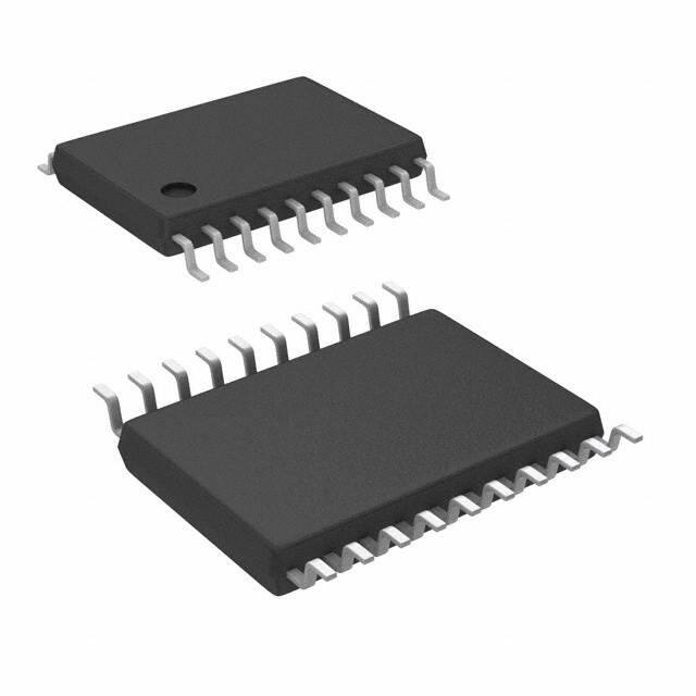
3. Ordering information
Table 1.
Ordering information
Type number
74AHC241D
Package
Temperature range
Name
Description
Version
−40 °C to +125 °C
SO20
plastic small outline package; 20 leads;
body width 7.5 mm
SOT163-1
−40 °C to +125 °C
TSSOP20
plastic thin shrink small outline package; 20 leads;
body width 4.4 mm
SOT360-1
−40 °C to +125 °C
DHVQFN20
plastic dual in-line compatible thermal enhanced
SOT764-1
very thin quad flat package; no leads; 20 terminals;
body 2.5 × 4.5 × 0.85 mm
74AHCT241D
74AHC241PW
74AHCT241PW
74AHC241BQ
74AHCT241BQ
�74AHC241; 74AHCT241
NXP Semiconductors
Octal buffer/line driver; 3-state
4. Functional diagram
1
2
1A0
1Y0
18
17
2A0
2Y0
3
4
1A1
1Y1
16
15
2A1
2Y1
5
6
1A2
1Y2
14
13
2A2
2Y2
7
8
1A3
1Y3
12
11
2A3
2Y3
9
1
1OE
19
2OE
2
18
4
16
6
14
8
12
19
mna771
EN
EN
11
9
13
7
15
5
17
3
mna773
Fig 1.
Logic symbol
Fig 2.
IEC logic symbol
5. Pinning information
5.1 Pinning
1
terminal 1
index area
74AHC241
74AHCT241
20 VCC
1OE
74AHC241
74AHCT241
1A0
2
19 2OE
2Y0
3
18 1Y0
1A1
4
17 2A0
1OE
1
20 VCC
1A0
2
19 2OE
2Y0
3
18 1Y0
2Y1
5
16 1Y1
1A1
4
17 2A0
1A2
6
15 2A1
2Y1
5
16 1Y1
2Y2
7
1A2
6
15 2A1
1A3
8
2Y2
7
14 1Y2
1A3
8
13 2A2
2Y3
9
2Y3
9
12 1Y3
GND 10
11 2A3
14 1Y2
GND(1)
13 2A2
2A3 11
GND 10
12 1Y3
001aal191
Transparent top view
001aal190
(1) The die substrate is attached to this pad using
conductive die attach material. It can not be used as a
supply pin or input. It is recommended that no
connection is made at all.
Fig 3.
Pin configuration SO20 and TSSOP20
Fig 4.
Pin configuration DHVQFN20
74AHC_AHCT241_1
Product data sheet
© NXP B.V. 2010. All rights reserved.
Rev. 01 — 11 January 2010
2 of 15
�74AHC241; 74AHCT241
NXP Semiconductors
Octal buffer/line driver; 3-state
5.2 Pin description
Table 2.
Pin description
Symbol
Pin
Description
1OE
1
output enable input (active LOW)
2OE
19
output enable input (active HIGH)
1A0, 1A1, 1A2, 1A3
2, 4, 6, 8
data input
2A0, 2A1, 2A2, 2A3
17, 15, 13, 11
data input
1Y0, 1Y1, 1Y2, 1Y3
18, 16, 14, 12
data output
2Y0, 2Y1, 2Y2, 2Y3
3, 5, 7, 9
data output
GND
10
ground (0 V)
VCC
20
power supply
6. Functional description
Table 3.
Function table[1]
Input
Output
Input
Output
1OE
1An
1Yn
2OE
2An
2Yn
L
L
L
H
L
L
L
H
H
H
H
H
H
X
Z
L
X
Z
[1]
H = HIGH voltage level; L = LOW voltage level; X = don’t care; Z = high-impedance OFF-state.
7. Limiting values
Table 4.
Limiting values
In accordance with the Absolute Maximum Rating System (IEC 60134). Voltages are referenced to GND (ground = 0 V).
Symbol
Parameter
VCC
VI
IIK
input clamping current
VI < −0.5 V
IOK
output clamping current
VO < −0.5 V or VO > VCC + 0.5 V
IO
output current
VO = −0.5 V to (VCC + 0.5 V)
ICC
supply current
IGND
ground current
Tstg
storage temperature
Ptot
[1]
[2]
Min
Max
Unit
supply voltage
−0.5
+7.0
V
input voltage
−0.5
+7.0
V
[1]
−20
-
mA
[1]
-
±20
mA
-
±25
mA
-
75
mA
−75
-
mA
−65
+150
°C
-
500
mW
total power dissipation
Conditions
Tamb = −40 °C to +125 °C
[2]
The minimum input and output voltage ratings may be exceeded if the input and output current ratings are observed.
For SO20 package: above 70 °C the value of Ptot derates linearly with 8.0 mW/K.
For TSSOP20 package: above 60 °C the value of Ptot derates linearly with 5.5 mW/K.
For DHVQFN20 package: above 60 °C the value of Ptot derates linearly with 4.5 mW/K.
74AHC_AHCT241_1
Product data sheet
© NXP B.V. 2010. All rights reserved.
Rev. 01 — 11 January 2010
3 of 15
�74AHC241; 74AHCT241
NXP Semiconductors
Octal buffer/line driver; 3-state
8. Recommended operating conditions
Table 5.
Recommended operating conditions
Symbol
Parameter
Conditions
Min
Typ
Max
Unit
74AHC241
VCC
supply voltage
2.0
5.0
5.5
V
VI
input voltage
0
-
5.5
V
VO
output voltage
0
-
VCC
V
Tamb
ambient temperature
−40
+25
+125
°C
Δt/ΔV
input transition rise and fall rate
VCC = 3.3 V ± 0.3 V
-
-
1 00
ns/V
VCC = 5 V ± 0.5 V
-
-
20
ns/V
74AHCT241
VCC
supply voltage
4.5
5.0
5.5
V
VI
input voltage
0
-
5.5
V
VO
output voltage
0
-
VCC
V
Tamb
ambient temperature
−40
+25
+125
°C
Δt/ΔV
input transition rise and fall rate
-
-
20
ns/V
VCC = 5 V ± 0.5 V
9. Static characteristics
Table 6.
Static characteristics
At recommended operating conditions; voltages are referenced to GND (ground = 0 V).
Symbol Parameter
25 °C
Conditions
−40 °C to +85 °C −40 °C to +125 °C Unit
Min
Typ
Max
Min
Max
Min
Max
1.5
-
-
1.5
-
1.5
-
V
VCC = 3.0 V
2.1
-
-
2.1
-
2.1
-
V
VCC = 5.5 V
3.85
-
-
3.85
-
3.85
-
V
VCC = 2.0 V
-
-
0.5
-
0.5
-
0.5
V
VCC = 3.0 V
-
-
0.9
-
0.9
-
0.9
V
74AHC241
VIH
VIL
VOH
VOL
HIGH-level
input voltage
LOW-level
input voltage
VCC = 2.0 V
VCC = 5.5 V
-
-
1.65
-
1.65
-
1.65
V
HIGH-level
VI = VIH or VIL
output voltage
IO = −50 μA; VCC = 2.0 V
1.9
2.0
-
1.9
-
1.9
-
V
IO = −50 μA; VCC = 3.0 V
2.9
3.0
-
2.9
-
2.9
-
V
IO = −50 μA; VCC = 4.5 V
4.4
4.5
-
4.4
-
4.4
-
V
IO = −4.0 mA; VCC = 3.0 V
2.58
-
-
2.48
-
2.40
-
V
IO = −8.0 mA; VCC = 4.5 V
3.94
-
-
3.80
-
3.70
-
V
LOW-level
VI = VIH or VIL
output voltage
IO = 50 μA; VCC = 2.0 V
-
0
0.1
-
0.1
-
0.1
V
IO = 50 μA; VCC = 3.0 V
-
0
0.1
-
0.1
-
0.1
V
IO = 50 μA; VCC = 4.5 V
-
0
0.1
-
0.1
-
0.1
V
IO = 4.0 mA; VCC = 3.0 V
-
-
0.36
-
0.44
-
0.55
V
IO = 8.0 mA; VCC = 4.5 V
-
-
0.36
-
0.44
-
0.55
V
74AHC_AHCT241_1
Product data sheet
© NXP B.V. 2010. All rights reserved.
Rev. 01 — 11 January 2010
4 of 15
�74AHC241; 74AHCT241
NXP Semiconductors
Octal buffer/line driver; 3-state
Table 6.
Static characteristics …continued
At recommended operating conditions; voltages are referenced to GND (ground = 0 V).
Symbol Parameter
25 °C
Conditions
−40 °C to +85 °C −40 °C to +125 °C Unit
Min
Typ
Max
Min
Max
Min
Max
II
input leakage
current
VI = 5.5 V or GND;
VCC = 0 V to 5.5 V
-
-
0.1
-
1.0
-
2.0
μA
IOZ
OFF-state
VI = VIH or VIL;
output current VO = VCC or GND;
VCC = 5.5 V
-
-
±0.25
-
±2.5
-
±10.0
μA
ICC
supply current VI = VCC or GND; IO = 0 A;
VCC = 5.5 V
-
-
4.0
-
40
-
80
μA
CI
input
capacitance
-
3
10
-
10
-
10
pF
CO
output
capacitance
-
4
-
-
-
-
-
pF
VI = VCC or GND
74AHCT241
VIH
HIGH-level
input voltage
VCC = 4.5 V to 5.5 V
2.0
-
-
2.0
-
2.0
-
V
VIL
LOW-level
input voltage
VCC = 4.5 V to 5.5 V
-
-
0.8
-
0.8
-
0.8
V
VOH
HIGH-level
VI = VIH or VIL; VCC = 4.5 V
output voltage
IO = −50 μA
4.4
4.5
-
4.4
-
4.4
-
V
3.94
-
-
3.80
-
3.70
-
V
-
0
0.1
-
0.1
-
0.1
V
-
-
0.36
-
0.44
-
0.55
V
-
-
0.1
-
1.0
-
2.0
μA
IO = −8.0 mA
VOL
LOW-level
VI = VIH or VIL; VCC = 4.5 V
output voltage
IO = 50 μA
IO = 8.0 mA
II
input leakage
current
VI = 5.5 V or GND;
VCC = 0 V to 5.5 V
IOZ
OFF-state
VI = VIH or VIL;
output current VO = VCC or GND per input
pin; other inputs at
VCC or GND; IO = 0 A;
VCC = 5.5 V
-
-
±0.25
-
±2.5
-
±10.0
μA
ICC
supply current VI = VCC or GND; IO = 0 A;
VCC = 5.5 V
-
-
4.0
-
40
-
80
μA
ΔICC
additional
per input pin;
supply current VI = VCC − 2.1 V;
other pins at VCC or GND;
IO = 0 A; VCC = 4.5 V to 5.5 V
-
-
1.35
-
1.5
-
1.5
mA
CI
input
capacitance
-
3
10
-
10
-
10
pF
CO
output
capacitance
-
4
-
-
-
-
-
pF
VI = VCC or GND
74AHC_AHCT241_1
Product data sheet
© NXP B.V. 2010. All rights reserved.
Rev. 01 — 11 January 2010
5 of 15
�74AHC241; 74AHCT241
NXP Semiconductors
Octal buffer/line driver; 3-state
10. Dynamic characteristics
Table 7.
Dynamic characteristics
Voltages are referenced to GND (ground = 0 V); for test circuit see Figure 8.
Symbol Parameter
25 °C
Conditions
Min
Typ[1]
VCC = 3.0 V to 3.6 V; CL = 15 pF
-
VCC = 3.0 V to 3.6 V; CL = 50 pF
-
VCC = 4.5 V to 5.5 V; CL = 15 pF
−40 °C to +125 °C
Unit
Max
Min
Max
Max
(85 °C) (125 °C)
4.5
8.4
1.0
9.7
11.5
ns
6.5
12.2
1.0
14.5
16.9
ns
-
3.2
5.4
1.0
6.2
7.8
ns
-
3.2
7.9
1.0
9.2
11.2
ns
VCC = 3.0 V to 3.6 V; CL = 15 pF
-
8.9
10.4
1.0
12.2
14.0
ns
VCC = 3.0 V to 3.6 V; CL = 50 pF
-
5.5
14.8
1.0
17.8
19.6
ns
VCC = 4.5 V to 5.5 V; CL = 15 pF
-
6.1
6.6
1.0
7.6
9.1
ns
-
3.9
9.4
1.0
11.0
12.2
ns
VCC = 3.0 V to 3.6 V; CL = 15 pF
-
6.5
10.4
1.0
12.2
14.0
ns
VCC = 3.0 V to 3.6 V; CL = 50 pF
-
5.6
14.8
1.0
17.8
19.6
ns
VCC = 4.5 V to 5.5 V; CL = 15 pF
-
3.2
6.6
1.0
7.6
9.1
ns
VCC = 4.5 V to 5.5 V; CL = 50 pF
-
4.0
9.4
1.0
11.0
12.2
ns
VCC = 3.0 V to 3.6 V; CL = 15 pF
-
5.1
10.2
1.0
11.8
13.3
ns
VCC = 3.0 V to 3.6 V; CL = 50 pF
-
7.2
14.4
1.0
15.8
19.2
ns
VCC = 4.5 V to 5.5 V; CL = 15 pF
-
3.6
7.3
1.0
8.2
9.2
ns
-
5.1
9.9
1.0
10.8
13.0
ns
VCC = 3.0 V to 3.6 V; CL = 15 pF
-
5.0
10.2
1.0
11.8
13.3
ns
VCC = 3.0 V to 3.6 V; CL = 50 pF
-
7.1
14.4
1.0
15.8
19.2
ns
VCC = 4.5 V to 5.5 V; CL = 15 pF
-
3.6
7.3
1.0
8.2
9.2
ns
-
5.1
9.9
1.0
10.8
13.0
ns
-
9
-
-
-
-
pF
VCC = 4.5 V to 5.5 V; CL = 15 pF
-
3.5
5.7
1.0
6.5
7.9
ns
VCC = 4.5 V to 5.5 V; CL = 50 pF
-
5.1
7.9
1.0
9.2
11.2
ns
74AHC241
tpd
propagation
delay
nAn to nYn; see Figure 5
[2]
VCC = 4.5 V to 5.5 V; CL = 50 pF
ten
enable time
1OE to 1Yn; see Figure 6
[2]
VCC = 4.5 V to 5.5 V; CL = 50 pF
2OE to 2Yn; see Figure 7
tdis
disable time
1OE to 1Yn; see Figure 6
[2]
[2]
VCC = 4.5 V to 5.5 V; CL = 50 pF
2OE to 2Yn; see Figure 7
[2]
VCC = 4.5 V to 5.5 V; CL = 50 pF
CPD
power
dissipation
capacitance
VI = GND to VCC; CL = 50 pF;
fi = 1 MHz
[3]
nAn to nYn; see Figure 5
[2]
74AHCT241
tpd
propagation
delay
74AHC_AHCT241_1
Product data sheet
© NXP B.V. 2010. All rights reserved.
Rev. 01 — 11 January 2010
6 of 15
�74AHC241; 74AHCT241
NXP Semiconductors
Octal buffer/line driver; 3-state
Table 7.
Dynamic characteristics …continued
Voltages are referenced to GND (ground = 0 V); for test circuit see Figure 8.
Symbol Parameter
ten
enable time
25 °C
Conditions
Max
Min
-
3.7
6.6
1.0
7.8
9.2
ns
-
5.4
9.5
1.0
11.1
12.4
ns
-
3.7
6.6
1.0
7.8
9.2
ns
-
5.4
9.5
1.0
11.1
12.4
ns
VCC = 4.5 V to 5.5 V; CL = 15 pF
-
4.8
7.8
1.0
8.8
9.7
ns
VCC = 4.5 V to 5.5 V; CL = 50 pF
-
7.1
10.5
1.0
11.4
13.5
ns
-
4.8
7.8
1.0
8.8
9.7
ns
-
7.1
10.5
1.0
11.4
13.5
ns
-
9
-
-
-
-
pF
[2]
2OE to 2Yn; see Figure 7
VCC = 4.5 V to 5.5 V; CL = 15 pF
VCC = 4.5 V to 5.5 V; CL = 50 pF
[2]
1OE to 1Yn; see Figure 6
[2]
2OE to 2Yn; see Figure 7
VCC = 4.5 V to 5.5 V; CL = 15 pF
VCC = 4.5 V to 5.5 V; CL = 50 pF
CPD
power
dissipation
capacitance
[3]
VI = GND to VCC; CL = 50 pF;
fi = 1 MHz
[1]
Typical values are measured at nominal supply voltage (VCC = 3.3 V and VCC = 5.0 V).
[2]
tpd is the same as tPLH and tPHL; ten is the same as tPZH and tPZL; tdis is the same as tPLZ and tPHZ.
[3]
Max
Max
(85 °C) (125 °C)
[2]
1OE to 1Yn; see Figure 6
VCC = 4.5 V to 5.5 V; CL = 50 pF
disable time
Unit
Min
VCC = 4.5 V to 5.5 V; CL = 15 pF
tdis
−40 °C to +125 °C
Typ[1]
CPD is used to determine the dynamic power dissipation (PD in μW).
PD = CPD × VCC2 × fi × N + ∑(CL × VCC2 × fo) where:
fi = input frequency in MHz;
fo = output frequency in MHz;
CL = output load capacitance in pF;
VCC = supply voltage in V;
N = number of inputs switching;
∑(CL × VCC2 × fo) = sum of outputs.
11. Waveforms
VI
nAn input
VM
VM
GND
tPHL
tPLH
VOH
VM
nYn output
VM
VOL
mgu781
Measurement points are given in Table 8.
VOL and VOH are typical voltage output drop that occur with the output load.
Fig 5.
Propagation delay input (nAn) to output (nYn)
74AHC_AHCT241_1
Product data sheet
© NXP B.V. 2010. All rights reserved.
Rev. 01 — 11 January 2010
7 of 15
�74AHC241; 74AHCT241
NXP Semiconductors
Octal buffer/line driver; 3-state
VI
1OE input
VM
GND
t PLZ
t PZL
VCC
output
LOW-to-OFF
OFF-to-LOW
VM
VX
VOL
t PZH
t PHZ
VOH
VY
output
HIGH-to-OFF
OFF-to-HIGH
VM
GND
outputs
enabled
outputs
enabled
outputs
disabled
mna775
Measurement points are given in Table 8.
VOL and VOH are typical voltage output levels that occur with the output load.
Fig 6.
Enable and disable times for input 1OE
VI
2OE input
VM
GND
t PLZ
t PZL
VCC
output
LOW-to-OFF
OFF-to-LOW
VM
VX
VOL
t PZH
t PHZ
VOH
output
HIGH-to-OFF
OFF-to-HIGH
VY
VM
GND
outputs
enabled
outputs
enabled
outputs
disabled
mna776
Measurement points are given in Table 8.
VOL and VOH are typical voltage output levels that occur with the output load.
Fig 7.
Enable and disable times for input 2OE
Table 8.
Measurement points
Type
Input
Output
VM
VM
VX
VY
74AHC241
0.5VCC
0.5VCC
VOL + 0.3 V
VOH − 0.3 V
74AHCT241
1.5 V
0.5VCC
VOL + 0.3 V
VOH − 0.3 V
74AHC_AHCT241_1
Product data sheet
© NXP B.V. 2010. All rights reserved.
Rev. 01 — 11 January 2010
8 of 15
�74AHC241; 74AHCT241
NXP Semiconductors
Octal buffer/line driver; 3-state
VI
tW
90 %
negative
pulse
VM
0V
tf
tr
tr
tf
VI
90 %
positive
pulse
0V
VM
10 %
VM
VM
10 %
tW
VCC
G
VI
VCC
VO
RL
S1
open
DUT
RT
CL
001aad983
Test data is given in Table 9.
Definitions test circuit:
RT = Termination resistance should be equal to output impedance Zo of the pulse generator.
CL = Load capacitance including jig and probe capacitance.
RL = Load resistance.
S1 = Test selection switch.
Fig 8.
Load circuitry for switching times
Table 9.
Test data
Type
Input
Load
S1 position
VI
tr, tf
CL
RL
tPHL, tPLH
tPZH, tPHZ
tPZL, tPLZ
74AHC241
VCC
3.0 ns
15 pF, 50 pF
1 kΩ
open
GND
VCC
74AHCT241
3.0 V
3.0 ns
15 pF, 50 pF
1 kΩ
open
GND
VCC
74AHC_AHCT241_1
Product data sheet
© NXP B.V. 2010. All rights reserved.
Rev. 01 — 11 January 2010
9 of 15
�74AHC241; 74AHCT241
NXP Semiconductors
Octal buffer/line driver; 3-state
12. Package outline
SO20: plastic small outline package; 20 leads; body width 7.5 mm
SOT163-1
D
E
A
X
c
HE
y
v M A
Z
20
11
Q
A2
A
(A 3)
A1
pin 1 index
θ
Lp
L
10
1
e
bp
detail X
w M
0
5
10 mm
scale
DIMENSIONS (inch dimensions are derived from the original mm dimensions)
UNIT
A
max.
A1
A2
A3
bp
c
D (1)
E (1)
e
HE
L
Lp
Q
v
w
y
mm
2.65
0.3
0.1
2.45
2.25
0.25
0.49
0.36
0.32
0.23
13.0
12.6
7.6
7.4
1.27
10.65
10.00
1.4
1.1
0.4
1.1
1.0
0.25
0.25
0.1
0.01
0.019 0.013
0.014 0.009
0.51
0.49
0.30
0.29
0.05
0.419
0.043
0.055
0.394
0.016
inches
0.1
0.012 0.096
0.004 0.089
0.043
0.039
0.01
0.01
Z
(1)
0.9
0.4
0.035
0.004
0.016
θ
8o
o
0
Note
1. Plastic or metal protrusions of 0.15 mm (0.006 inch) maximum per side are not included.
Fig 9.
REFERENCES
OUTLINE
VERSION
IEC
JEDEC
SOT163-1
075E04
MS-013
JEITA
EUROPEAN
PROJECTION
ISSUE DATE
99-12-27
03-02-19
Package outline SOT163-1 (SO20)
74AHC_AHCT241_1
Product data sheet
© NXP B.V. 2010. All rights reserved.
Rev. 01 — 11 January 2010
10 of 15
�74AHC241; 74AHCT241
NXP Semiconductors
Octal buffer/line driver; 3-state
TSSOP20: plastic thin shrink small outline package; 20 leads; body width 4.4 mm
SOT360-1
E
D
A
X
c
HE
y
v M A
Z
11
20
Q
A2
(A 3)
A1
pin 1 index
A
θ
Lp
L
1
10
e
detail X
w M
bp
0
2.5
5 mm
scale
DIMENSIONS (mm are the original dimensions)
UNIT
A
max.
A1
A2
A3
bp
c
D (1)
E (2)
e
HE
L
Lp
Q
v
w
y
Z (1)
θ
mm
1.1
0.15
0.05
0.95
0.80
0.25
0.30
0.19
0.2
0.1
6.6
6.4
4.5
4.3
0.65
6.6
6.2
1
0.75
0.50
0.4
0.3
0.2
0.13
0.1
0.5
0.2
8
o
0
o
Notes
1. Plastic or metal protrusions of 0.15 mm maximum per side are not included.
2. Plastic interlead protrusions of 0.25 mm maximum per side are not included.
OUTLINE
VERSION
SOT360-1
REFERENCES
IEC
JEDEC
JEITA
EUROPEAN
PROJECTION
ISSUE DATE
99-12-27
03-02-19
MO-153
Fig 10. Package outline SOT360-1 (TSSOP20)
74AHC_AHCT241_1
Product data sheet
© NXP B.V. 2010. All rights reserved.
Rev. 01 — 11 January 2010
11 of 15
�74AHC241; 74AHCT241
NXP Semiconductors
Octal buffer/line driver; 3-state
DHVQFN20: plastic dual in-line compatible thermal enhanced very thin quad flat package; no leads;
SOT764-1
20 terminals; body 2.5 x 4.5 x 0.85 mm
A
B
D
A
A1
E
c
detail X
terminal 1
index area
terminal 1
index area
C
e1
e
2
9
y
y1 C
v M C A B
w M C
b
L
1
10
Eh
e
20
11
19
12
Dh
X
0
2.5
5 mm
scale
DIMENSIONS (mm are the original dimensions)
UNIT
A(1)
max.
A1
b
c
D (1)
Dh
E (1)
Eh
e
e1
L
v
w
y
y1
mm
1
0.05
0.00
0.30
0.18
0.2
4.6
4.4
3.15
2.85
2.6
2.4
1.15
0.85
0.5
3.5
0.5
0.3
0.1
0.05
0.05
0.1
Note
1. Plastic or metal protrusions of 0.075 mm maximum per side are not included.
REFERENCES
OUTLINE
VERSION
IEC
JEDEC
JEITA
SOT764-1
---
MO-241
---
EUROPEAN
PROJECTION
ISSUE DATE
02-10-17
03-01-27
Fig 11. Package outline SOT764-1 (DHVQFN20)
74AHC_AHCT241_1
Product data sheet
© NXP B.V. 2010. All rights reserved.
Rev. 01 — 11 January 2010
12 of 15
�74AHC241; 74AHCT241
NXP Semiconductors
Octal buffer/line driver; 3-state
13. Abbreviations
Table 10.
Abbreviations
Acronym
Description
CDM
Charge Device Model
CMOS
Complementary Metal Oxide Semiconductor
DUT
Device Under Test
ESD
ElectroStatic Discharge
HBM
Human Body Model
TTL
Transistor-Transistor Logic
14. Revision history
Table 11.
Revision history
Document ID
Release date
Data sheet status
Change notice
Supersedes
74AHC_AHCT241_1
20100111
Product data sheet
-
-
74AHC_AHCT241_1
Product data sheet
© NXP B.V. 2010. All rights reserved.
Rev. 01 — 11 January 2010
13 of 15
�74AHC241; 74AHCT241
NXP Semiconductors
Octal buffer/line driver; 3-state
15. Legal information
15.1 Data sheet status
Document status[1][2]
Product status[3]
Definition
Objective [short] data sheet
Development
This document contains data from the objective specification for product development.
Preliminary [short] data sheet
Qualification
This document contains data from the preliminary specification.
Product [short] data sheet
Production
This document contains the product specification.
[1]
Please consult the most recently issued document before initiating or completing a design.
[2]
The term ‘short data sheet’ is explained in section “Definitions”.
[3]
The product status of device(s) described in this document may have changed since this document was published and may differ in case of multiple devices. The latest product status
information is available on the Internet at URL http://www.nxp.com.
15.2 Definitions
Draft — The document is a draft version only. The content is still under
internal review and subject to formal approval, which may result in
modifications or additions. NXP Semiconductors does not give any
representations or warranties as to the accuracy or completeness of
information included herein and shall have no liability for the consequences of
use of such information.
Short data sheet — A short data sheet is an extract from a full data sheet
with the same product type number(s) and title. A short data sheet is intended
for quick reference only and should not be relied upon to contain detailed and
full information. For detailed and full information see the relevant full data
sheet, which is available on request via the local NXP Semiconductors sales
office. In case of any inconsistency or conflict with the short data sheet, the
full data sheet shall prevail.
15.3 Disclaimers
General — Information in this document is believed to be accurate and
reliable. However, NXP Semiconductors does not give any representations or
warranties, expressed or implied, as to the accuracy or completeness of such
information and shall have no liability for the consequences of use of such
information.
Right to make changes — NXP Semiconductors reserves the right to make
changes to information published in this document, including without
limitation specifications and product descriptions, at any time and without
notice. This document supersedes and replaces all information supplied prior
to the publication hereof.
Suitability for use — NXP Semiconductors products are not designed,
authorized or warranted to be suitable for use in medical, military, aircraft,
space or life support equipment, nor in applications where failure or
malfunction of an NXP Semiconductors product can reasonably be expected
to result in personal injury, death or severe property or environmental
damage. NXP Semiconductors accepts no liability for inclusion and/or use of
NXP Semiconductors products in such equipment or applications and
therefore such inclusion and/or use is at the customer’s own risk.
Applications — Applications that are described herein for any of these
products are for illustrative purposes only. NXP Semiconductors makes no
representation or warranty that such applications will be suitable for the
specified use without further testing or modification.
Limiting values — Stress above one or more limiting values (as defined in
the Absolute Maximum Ratings System of IEC 60134) may cause permanent
damage to the device. Limiting values are stress ratings only and operation of
the device at these or any other conditions above those given in the
Characteristics sections of this document is not implied. Exposure to limiting
values for extended periods may affect device reliability.
Terms and conditions of sale — NXP Semiconductors products are sold
subject to the general terms and conditions of commercial sale, as published
at http://www.nxp.com/profile/terms, including those pertaining to warranty,
intellectual property rights infringement and limitation of liability, unless
explicitly otherwise agreed to in writing by NXP Semiconductors. In case of
any inconsistency or conflict between information in this document and such
terms and conditions, the latter will prevail.
No offer to sell or license — Nothing in this document may be interpreted or
construed as an offer to sell products that is open for acceptance or the grant,
conveyance or implication of any license under any copyrights, patents or
other industrial or intellectual property rights.
Export control — This document as well as the item(s) described herein
may be subject to export control regulations. Export might require a prior
authorization from national authorities.
15.4 Trademarks
Notice: All referenced brands, product names, service names and trademarks
are the property of their respective owners.
16. Contact information
For more information, please visit: http://www.nxp.com
For sales office addresses, please send an email to: salesaddresses@nxp.com
74AHC_AHCT241_1
Product data sheet
© NXP B.V. 2010. All rights reserved.
Rev. 01 — 11 January 2010
14 of 15
�NXP Semiconductors
74AHC241; 74AHCT241
Octal buffer/line driver; 3-state
17. Contents
1
2
3
4
5
5.1
5.2
6
7
8
9
10
11
12
13
14
15
15.1
15.2
15.3
15.4
16
17
General description . . . . . . . . . . . . . . . . . . . . . . 1
Features . . . . . . . . . . . . . . . . . . . . . . . . . . . . . . . 1
Ordering information . . . . . . . . . . . . . . . . . . . . . 1
Functional diagram . . . . . . . . . . . . . . . . . . . . . . 2
Pinning information . . . . . . . . . . . . . . . . . . . . . . 2
Pinning . . . . . . . . . . . . . . . . . . . . . . . . . . . . . . . 2
Pin description . . . . . . . . . . . . . . . . . . . . . . . . . 3
Functional description . . . . . . . . . . . . . . . . . . . 3
Limiting values. . . . . . . . . . . . . . . . . . . . . . . . . . 3
Recommended operating conditions. . . . . . . . 4
Static characteristics. . . . . . . . . . . . . . . . . . . . . 4
Dynamic characteristics . . . . . . . . . . . . . . . . . . 6
Waveforms . . . . . . . . . . . . . . . . . . . . . . . . . . . . . 7
Package outline . . . . . . . . . . . . . . . . . . . . . . . . 10
Abbreviations . . . . . . . . . . . . . . . . . . . . . . . . . . 13
Revision history . . . . . . . . . . . . . . . . . . . . . . . . 13
Legal information. . . . . . . . . . . . . . . . . . . . . . . 14
Data sheet status . . . . . . . . . . . . . . . . . . . . . . 14
Definitions . . . . . . . . . . . . . . . . . . . . . . . . . . . . 14
Disclaimers . . . . . . . . . . . . . . . . . . . . . . . . . . . 14
Trademarks. . . . . . . . . . . . . . . . . . . . . . . . . . . 14
Contact information. . . . . . . . . . . . . . . . . . . . . 14
Contents . . . . . . . . . . . . . . . . . . . . . . . . . . . . . . 15
Please be aware that important notices concerning this document and the product(s)
described herein, have been included in section ‘Legal information’.
© NXP B.V. 2010.
All rights reserved.
For more information, please visit: http://www.nxp.com
For sales office addresses, please send an email to: salesaddresses@nxp.com
Date of release: 11 January 2010
Document identifier: 74AHC_AHCT241_1
�


 工商网监
湘ICP备2023018690号
工商网监
湘ICP备2023018690号
