NXP Semiconductors
Technical Data
Document Number: AFT27S012N
Rev. 0, 07/2017
RF Power LDMOS Transistor
N--Channel Enhancement--Mode Lateral MOSFET
AFT27S012NT1
This 1.26 W RF power LDMOS transistor is designed for cellular base
station applications covering the frequency range of 728 to 2700 MHz.
Typical Single--Carrier W--CDMA Performance: VDD = 28 Vdc,
IDQ = 90 mA, Pout = 1.26 W Avg., Input Signal PAR = 9.9 dB @ 0.01%
Probability on CCDF.(1)
2100 MHz
Frequency
Gps
(dB)
D
(%)
Output PAR
(dB)
ACPR
(dBc)
IRL
(dB)
2110 MHz
20.8
22.0
9.8
–41.1
–9
2140 MHz
20.9
22.6
9.6
–40.7
–10
2170 MHz
20.9
22.8
9.4
–40.8
–10
2200 MHz
20.8
22.9
9.3
–40.4
–9
728–2700 MHz, 1.26 W AVG., 28 V
AIRFAST RF POWER LDMOS
TRANSISTOR
PLD--1.5W
PLASTIC
1. All data measured in fixture with device soldered to heatsink.
Features
Greater negative gate--source voltage range for improved Class C operation
Designed for digital predistortion error correction systems
Universal broadband driven device with internal RF feedback
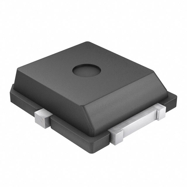
RFin/VGS
RFout/VDS
(Top View)
Note: The center pad on the backside of the
package is the source terminal for the
transistor.
Figure 1. Pin Connections
2017 NXP B.V.
RF Device Data
NXP Semiconductors
AFT27S012NT1
1
�Table 1. Maximum Ratings
Symbol
Value
Unit
Drain--Source Voltage
Rating
VDSS
--0.5, +65
Vdc
Gate--Source Voltage
VGS
--6.0, +10
Vdc
Operating Voltage
VDD
32, +0
Vdc
Storage Temperature Range
Tstg
--65 to +150
C
Case Operating Temperature Range
TC
--40 to +150
C
(1,2)
TJ
--40 to +150
C
Characteristic
Symbol
Value (2,3)
Unit
RJC
3.4
C/W
Operating Junction Temperature Range
Table 2. Thermal Characteristics
Thermal Resistance, Junction to Case
Case Temperature 77C, 1.3 W CW, 28 Vdc, IDQ = 110 mA, 2450 MHz
Table 3. ESD Protection Characteristics
Test Methodology
Class
Human Body Model (per JESD22--A114)
1B
Charge Device Model (per JESD22--C101)
C3
Table 4. Moisture Sensitivity Level
Test Methodology
Per JESD22--A113, IPC/JEDEC J--STD--020
Rating
Package Peak Temperature
Unit
3
260
C
Table 5. Electrical Characteristics (TA = 25C unless otherwise noted)
Symbol
Min
Typ
Max
Unit
Zero Gate Voltage Drain Leakage Current
(VDS = 65 Vdc, VGS = 0 Vdc)
IDSS
—
—
10
Adc
Zero Gate Voltage Drain Leakage Current
(VDS = 32 Vdc, VGS = 0 Vdc)
IDSS
—
—
1
Adc
Gate--Source Leakage Current
(VGS = 5 Vdc, VDS = 0 Vdc)
IGSS
—
—
1
Adc
Gate Threshold Voltage
(VDS = 10 Vdc, ID = 15.4 Adc)
VGS(th)
0.8
1.2
1.6
Vdc
Gate Quiescent Voltage
(VDD = 28 Vdc, ID = 90 mAdc, Measured in Functional Test)
VGS(Q)
1.5
1.8
2.3
Vdc
Drain--Source On--Voltage
(VGS = 10 Vdc, ID = 154 mAdc)
VDS(on)
0.1
0.2
0.3
Vdc
Characteristic
Off Characteristics
On Characteristics
1. Continuous use at maximum temperature will affect MTTF.
2. MTTF calculator available at http://www.nxp.com/RF/calculators.
3. Refer to AN1955, Thermal Measurement Methodology of RF Power Amplifiers. Go to http://www.nxp.com/RF and search for AN1955.
(continued)
AFT27S012NT1
2
RF Device Data
NXP Semiconductors
�Table 5. Electrical Characteristics (TA = 25C unless otherwise noted) (continued)
Characteristic
Symbol
Min
Typ
Max
Unit
Functional Tests (In NXP Test Fixture, 50 ohm system) VDD = 28 Vdc, IDQ = 90 mA, Pout = 1.26 W Avg., f = 2170 MHz, Single--Carrier
W--CDMA, IQ Magnitude Clipping, Input Signal PAR = 9.9 dB @ 0.01% Probability on CCDF. ACPR measured in 3.84 MHz Channel
Bandwidth @ 5 MHz Offset.
Power Gain
Gps
20.0
20.9
—
dB
Drain Efficiency
D
18.5
22.8
—
%
ACPR
—
--40.8
–37.9
dBc
IRL
—
--12
–9
dB
Adjacent Channel Power Ratio
Input Return Loss
Load Mismatch (In NXP Test Fixture, 50 ohm system) IDQ = 90 mA, f = 2140 MHz
VSWR 10:1 at 32 Vdc, 16.6 W CW Output Power
(3 dB Input Overdrive from 125 mW CW Rated Power)
No Device Degradation
Typical Performance(1) (In NXP Test Fixture, 50 ohm system) VDD = 28 Vdc, IDQ = 90 mA, 2110--2200 MHz Bandwidth
Pout @ 1 dB Compression Point, CW
P1dB
—
13
—
W
AM/PM
(Maximum value measured at the P3dB compression point across
the 2110--2200 MHz frequency range.)
—
–13
—
Gain Flatness in 90 MHz Bandwidth @ Pout = 1.26 W Avg.
GF
—
0.20
—
dB
Gain Variation over Temperature
(--30C to +85C)
G
—
0.004
—
dB/C
P1dB
—
0.010
—
dB/C
Output Power Variation over Temperature
(--30C to +85C)
Table 6. Ordering Information
Device
AFT27S012NT1
Tape and Reel Information
T1 Suffix = 1000 Units, 16 mm Tape Width, 7--inch Reel
Package
PLD--1.5W
1. All data measured in fixture with device soldered to heatsink.
AFT27S012NT1
RF Device Data
NXP Semiconductors
3
�VGG
VDD
C7
C13
C6
C12
C8
R1
C1*
Q1
C2
C5*
C4
C3
C9
AFT27S010N
Rev. 2
2100MHz
C10
C11
D53402
VDD
*C1 and C5 are mounted vertically.
NOTE: All data measured in fixture with device soldered to heatsink. AFT27S012N uses the AFT27S0101N production fixture;
board and parts list are identical.
Figure 2. AFT27S010NT1 Test Circuit Component Layout — 2110--2200 MHz
Table 7. AFT27S010NT1 Test Circuit Component Designations and Values — 2110--2200 MHz
Part
Description
Part Number
Manufacturer
C1, C5, C6, C8, C9
9.1 pF Chip Capacitors
ATC100B9R1JT500XT
ATC
C2
1.1 pF Chip Capacitor
ATC100B1R1JT500XT
ATC
C3
2.0 pF Chip Capacitor
ATC100B2R0JT500XT
ATC
C4
1.0 pF Chip Capacitor
ATC100B1R0JT500XT
ATC
C7, C10, C11, C12, C13
10 F Chip Capacitors
GRM32ER61H106KA12L
Murata
Q1
RF Power LDMOS Transistor
AFT27S010N
NXP
R1
2.37 Chip Resistor
CRCW12062R37FKEA
Vishay
PCB
Rogers RO4350B, 0.020, r = 3.66
D53402
MTL
AFT27S012NT1
4
RF Device Data
NXP Semiconductors
�0.28
7.11
0.165
4.91
0.089
2.26
Solder pad with thermal via
structure. All dimensions in mm.
0.155
3.94
0.085
2.16
Figure 3. PCB Pad Layout for PLD--1.5W
AFS12
N(
)A
WLYWWZ
Figure 4. Product Marking
AFT27S012NT1
RF Device Data
NXP Semiconductors
5
�PACKAGE DIMENSIONS
AFT27S012NT1
6
RF Device Data
NXP Semiconductors
�AFT27S012NT1
RF Device Data
NXP Semiconductors
7
�AFT27S012NT1
8
RF Device Data
NXP Semiconductors
�PRODUCT DOCUMENTATION
Refer to the following resources to aid your design process.
Application Notes
AN1907: Solder Reflow Attach Method for High Power RF Devices in Plastic Packages
AN1955: Thermal Measurement Methodology of RF Power Amplifiers
Engineering Bulletins
EB212: Using Data Sheet Impedances for RF LDMOS Devices
To Download Resources Specific to a Given Part Number:
1. Go to http://www.nxp.com/RF
2. Search by part number
3. Click part number link
4. Choose the desired resource from the drop down menu
REVISION HISTORY
The following table summarizes revisions to this document.
Revision
Date
0
July 2017
Description
Initial release of data sheet
AFT27S012NT1
RF Device Data
NXP Semiconductors
9
�How to Reach Us:
Home Page:
nxp.com
Web Support:
nxp.com/support
Information in this document is provided solely to enable system and software
implementers to use NXP products. There are no express or implied copyright licenses
granted hereunder to design or fabricate any integrated circuits based on the information
in this document. NXP reserves the right to make changes without further notice to any
products herein.
NXP makes no warranty, representation, or guarantee regarding the suitability of its
products for any particular purpose, nor does NXP assume any liability arising out of the
application or use of any product or circuit, and specifically disclaims any and all liability,
including without limitation consequential or incidental damages. “Typical” parameters
that may be provided in NXP data sheets and/or specifications can and do vary in
different applications, and actual performance may vary over time. All operating
parameters, including “typicals,” must be validated for each customer application by
customer’s technical experts. NXP does not convey any license under its patent rights
nor the rights of others. NXP sells products pursuant to standard terms and conditions of
sale, which can be found at the following address: nxp.com/SalesTermsandConditions.
NXP, the NXP logo, Freescale, the Freescale logo, and Airfast are trademarks of
NXP B.V. All other product or service names are the property of their respective owners.
E 2017 NXP B.V.
AFT27S012NT1
Document Number: AFT27S012N
Rev. 0, 07/2017
10
RF Device Data
NXP Semiconductors
�


 工商网监
湘ICP备2023018690号
工商网监
湘ICP备2023018690号
