BLF878
UHF power LDMOS transistor
Rev. 02 — 15 June 2009
Product data sheet
1. Product profile
1.1 General description
A 300 W LDMOS RF power transistor for broadcast transmitter applications and industrial
applications. The transistor can deliver 300 W broadband over the full UHF band from
470 MHz to 860 MHz. The excellent ruggedness and broadband performance of this
device makes it ideal for digital transmitter applications.
Table 1.
Typical performance
RF performance at VDS = 42 V in a common-source 860 MHz narrowband test circuit.
Mode of operation f
PL
PL(PEP) PL(AV) Gp
(MHz)
(W)
(W)
CW, class AB
860
300
2-Tone, class AB
f1 = 860; f2 = 860.1 -
PAL BG
860 (ch69)
300 (peak sync.)
DVB-T (8k OFDM)
858
-
[1]
(W)
ηD
IMD3
(dB) (%) (dBc)
-
-
21
60
-
300
-
21
46
−35
-
-
21
45
-
-
75
21
32
−32 [2]
[1]
Black video signal, sync expansion: input sync = 33 %; output sync ≥ 27 %.
[2]
Measured [dBc] with delta marker at 4.3 MHz from center frequency.
CAUTION
This device is sensitive to ElectroStatic Discharge (ESD). Therefore care should be taken
during transport and handling.
1.2 Features
n 2-Tone performance at 860 MHz, a drain-source voltage VDS of 42 V and a quiescent
drain current IDq = 1.4 A:
u Peak envelope power load power = 300 W
u Power gain = 21 dB
u Drain efficiency = 46 %
u Third order intermodulation distortion = −35 dBc
n DVB performance at 858 MHz, a drain-source voltage VDS of 42 V and a quiescent
drain current IDq = 1.4 A:
u Average output power = 75 W
u Power gain = 21 dB
u Drain efficiency = 32 %
u Third order intermodulation distortion = −32 dBc (4.3 MHz from center frequency)
�BLF878
NXP Semiconductors
UHF power LDMOS transistor
n
n
n
n
n
n
n
n
n
n
Integrated ESD protection
Advanced flange material for optimum thermal behavior and reliability
Excellent ruggedness
High power gain
High efficiency
Designed for broadband operation (470 MHz to 860 MHz)
Excellent reliability
Internal input and output matching for high gain and optimum broadband operation
Easy power control
Compliant to Directive 2002/95/EC, regarding Restriction of Hazardous Substances
(RoHS)
1.3 Applications
n Communication transmitter applications in the UHF band
n Industrial applications in the UHF band
2. Pinning information
Table 2.
Pinning
Pin
Description
1
drain1
2
drain2
3
gate1
4
gate2
5
Simplified outline
1
Graphic symbol
2
1
5
3
3
[1]
source
5
4
4
2
sym117
[1]
Connected to flange.
3. Ordering information
Table 3.
Ordering information
Type number Package
Name Description
BLF878
-
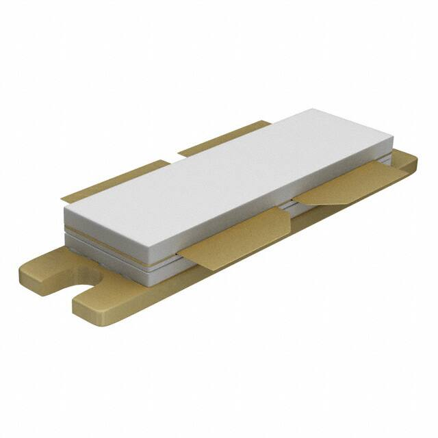
flanged LDMOST ceramic package; 2 mounting holes; 4 leads SOT979A
BLF878_2
Product data sheet
Version
© NXP B.V. 2009. All rights reserved.
Rev. 02 — 15 June 2009
2 of 18
�BLF878
NXP Semiconductors
UHF power LDMOS transistor
4. Limiting values
Table 4.
Limiting values
In accordance with the Absolute Maximum Rating System (IEC 60134).
Symbol
Parameter
VDS
Conditions
Min
Max
Unit
drain-source voltage
-
89
V
VGS
gate-source voltage
−0.5
+11
V
Tstg
storage temperature
−65
+150
°C
Tj
junction temperature
-
200
°C
5. Thermal characteristics
Table 5.
Thermal characteristics
Symbol
Parameter
Conditions
Rth(j-c)
thermal resistance from junction to case
Tcase = 80 °C;
PL(AV) = 150 W
Rth(c-h)
thermal resistance from case to heatsink
Typ
Unit
[1]
0.23
K/W
[2]
0.15
K/W
[1]
Rth(j-c) is measured under RF conditions.
[2]
Rth(c-h) is dependent on the applied thermal compound and clamping/mounting of the device.
6. Characteristics
Table 6.
Characteristics
Tj = 25 °C unless otherwise specified.
Symbol Parameter
Conditions
V(BR)DSS drain-source breakdown voltage VGS = 0 V; ID = 2.25 mA
Unit
89
-
105.5 V
[1]
1.4
1.9
2.4
V
VGS(th)
gate-source threshold voltage
VDS = 10 V; ID = 225 mA
IDSS
drain leakage current
VGS = 0 V; VDS = 42 V
-
-
1.4
µA
IDSX
drain cut-off current
VGS = VGSth + 3.75 V;
VDS = 10 V
35
39
-
A
IGSS
gate leakage current
VGS = 11 V; VDS = 0 V
140
nA
forward transconductance
gfs
VDS = 10 V; ID = 11.2 A
-
-
[1]
-
15.5 -
S
-
110
-
mΩ
RDS(on)
drain-source on-state resistance VGS = VGSth + 3.75 V;
ID = 7.6 A
[1]
Ciss
input capacitance
VGS = 0 V; VDS = 40 V;
f = 1 MHz
[2]
-
190
-
pF
Coss
output capacitance
VGS = 0 V; VDS = 40 V;
f = 1 MHz
[2]
-
60
-
pF
Crss
reverse transfer capacitance
VGS = 0 V; VDS = 40 V;
f = 1 MHz
[2]
-
2
-
pF
[1]
ID is the drain current.
[2]
Capacitance values without internal matching.
BLF878_2
Product data sheet
Min Typ Max
[1]
© NXP B.V. 2009. All rights reserved.
Rev. 02 — 15 June 2009
3 of 18
�BLF878
NXP Semiconductors
UHF power LDMOS transistor
001aai075
350
Coss
(pF)
250
150
50
0
20
40
60
VDS (V)
VGS = 0 V; f = 1 MHz.
Fig 1.
Output capacitance as a function of drain-source voltage; typical values per
section; capacitance value without internal matching
7. Application information
Table 7.
RF performance in a common-source narrowband 860 MHz test circuit
Tcase = 25 °C unless otherwise specified.
Mode of operation
f
2-Tone, class AB
DVB-T (8k OFDM)
858
PL(PEP)
PL(AV) Gp
(MHz)
(V)
(A)
(W)
(W)
(dB) (%)
f1 = 860; f2 = 860.1
40
1.4[1] 300
-
> 18 > 42 < −31
40
1.4[1] -
75
> 18 > 29 < −29 [2]
[1]
IDq = 1.4 A for total device.
[2]
Measured [dBc] with delta marker at 4.3 MHz from center frequency.
BLF878_2
Product data sheet
ηD
VDS IDq
IMD3
(dBc)
© NXP B.V. 2009. All rights reserved.
Rev. 02 — 15 June 2009
4 of 18
�BLF878
NXP Semiconductors
UHF power LDMOS transistor
7.1 Narrowband RF figures
7.1.1 CW
001aai076
24
Gp
(dB)
80
ηD
(%)
(2)
(1)
22
60
Gp
(2)
20
ηD
40
(1)
18
20
16
0
100
200
0
400
300
PL (W)
IDq = 1.4 A; measured in a common source narrowband 860 MHz test circuit.
(1) VDS = 40 V
(2) VDS = 42 V
Fig 2.
CW power gain and drain efficiency as a function of load power; typical values
BLF878_2
Product data sheet
© NXP B.V. 2009. All rights reserved.
Rev. 02 — 15 June 2009
5 of 18
�BLF878
NXP Semiconductors
UHF power LDMOS transistor
7.1.2 2-Tone
001aai077
22
Gp
Gp
(dB)
60
(1)
ηD
(%)
(2)
001aai078
−10
IMD3
(dBc)
−20
20
(2)
ηD
40
(1)
−30
(1)
(2)
20
18
−40
16
0
100
200
0
300
400
PL(AV) (W)
−50
0
IDq = 1.4 A; measured in a common source narrowband
860 MHz test circuit.
100
(1) VDS = 40 V
(2) VDS = 42 V
(2) VDS = 42 V
2-Tone power gain and drain efficiency as
functions of average load power; typical
values
Fig 4.
2-Tone third order intermodulation distortion
as a function of average load power; typical
values
BLF878_2
Product data sheet
300
400
PL(AV) (W)
IDq = 1.4 A; measured in a common source narrowband
860 MHz test circuit.
(1) VDS = 40 V
Fig 3.
200
© NXP B.V. 2009. All rights reserved.
Rev. 02 — 15 June 2009
6 of 18
�BLF878
NXP Semiconductors
UHF power LDMOS transistor
7.1.3 DVB-T
001aai079
23
Gp
(dB)
60
ηD
(%)
(2)
(1)
Gp
21
001aai080
−15
IMD3
(dBc)
40
−25
20
−35
(1)
(2)
ηD
19
(1)
(2)
17
0
50
100
150
0
200
250
PL(AV) (W)
−45
0
IDq = 1.4 A; measured in a common source narrowband
860 MHz test circuit.
50
(1) VDS = 40 V
(2) VDS = 42 V
(2) VDS = 42 V
DVB-T power gain and drain efficiency as
functions of average load power; typical
values
Fig 6.
200
250
PL(AV) (W)
DVB-T third order intermodulation distortion
as a function of average load power; typical
values
BLF878_2
Product data sheet
150
IDq = 1.4 A; measured in a common source narrowband
860 MHz test circuit.
(1) VDS = 40 V
Fig 5.
100
© NXP B.V. 2009. All rights reserved.
Rev. 02 — 15 June 2009
7 of 18
�BLF878
NXP Semiconductors
UHF power LDMOS transistor
7.2 Broadband RF figures
7.2.1 2-Tone
001aai081
22
Gp
(dB)
(2)
(1)
Gp
18
80
ηD
(%)
60
14
−20
(1)
(2)
40
500
IMD3
(dBc)
(1)
(2)
ηD
10
400
001aai082
0
600
700
20
800
900
f (MHz)
−40
−60
400
PL(AV) = 150 W; IDq = 1.4 A; measured in a common
source broadband test circuit as described in Section 8.
500
(1) VDS = 40 V
(2) VDS = 42 V
(2) VDS = 42 V
2-Tone power gain and drain efficiency as a
function of frequency; typical values
Fig 8.
800
900
f (MHz)
2-Tone third order intermodulation distortion
as a function of frequency; typical values
BLF878_2
Product data sheet
700
PL(AV) = 150 W; IDq = 1.4 A; measured in a common
source broadband test circuit as described in Section 8.
(1) VDS = 40 V
Fig 7.
600
© NXP B.V. 2009. All rights reserved.
Rev. 02 — 15 June 2009
8 of 18
�BLF878
NXP Semiconductors
UHF power LDMOS transistor
7.2.2 DVB-T
001aai083
22
60
ηD
(%)
(2)
(1)
Gp
(dB)
Gp
18
IMD3
(dBc)
−20
40
(1)
(2)
ηD
(1)
(2)
−40
20
14
10
400
500
600
001aai084
0
−60
400
0
800
900
f (MHz)
700
PL(AV) = 77 W; IDq = 1.4 A; measured in a common
source broadband test circuit as described in Section 8.
500
(1) VDS = 40 V
(2) VDS = 42 V
(2) VDS = 42 V
DVB-T power gain and drain efficiency as
functions of frequency; typical values
700
800
900
f (MHz)
PL(AV) = 77 W; IDq = 1.4 A; measured in a common
source broadband test circuit as described in Section 8.
(1) VDS = 40 V
Fig 9.
600
Fig 10. DVB-T third order intermodulation distortion
as a function of frequency; typical values
001aai085
10
PAR
(dB)
9
(2)
(1)
8
7
6
5
400
500
600
700
800
900
f (MHz)
PL(AV) = 77 W; IDq = 1.4 A; measured in a common source broadband test circuit as described in Section 8.
PAR of input signal = 9.5 dB at 0.01 % probability on CCDF.
(1) VDS = 40 V
(2) VDS = 42 V
Fig 11. DVB-T PAR at 0.1 % and at 0.01 % probability on the CCDF as function of frequency; typical values
BLF878_2
Product data sheet
© NXP B.V. 2009. All rights reserved.
Rev. 02 — 15 June 2009
9 of 18
�BLF878
NXP Semiconductors
UHF power LDMOS transistor
7.3 Ruggedness in class-AB operation
The BLF878 is capable of withstanding a load mismatch corresponding to VSWR = 10 : 1
through all phases under the following conditions: VDS = 42 V; f = 860 MHz at rated
power.
7.4 Impedance information
ZL
drain
Zi
gate
001aai086
Fig 12. Definition of transistor impedance
Table 8.
Typical push-pull impedance
Simulated Zi and ZL device impedance; impedance info at VDS = 42 V and PL(PEP) = 300 W.
f
Zi
ZL
MHz
Ω
Ω
300
0.933 − j1.376
6.431 − j4.296
325
0.959 − j0.986
6.889 − j3.911
350
0.988 − j0.628
7.237 − j3.476
375
1.020 − j0.295
7.475 − j3.017
400
1.057 + j0.017
7.610 − j2.559
425
1.097 + j0.314
7.652 − j2.120
450
1.143 + j0.598
7.614 − j1.713
475
1.194 + j0.871
7.512 − j1.348
500
1.251 + j1.137
7.359 − j1.031
525
1.315 + j1.397
7.168 − j0.762
550
1.388 + j1.652
6.949 − j0.542
575
1.470 + j1.903
6.712 − j0.368
600
1.563 + j2.152
6.465 − j0.237
625
1.668 + j2.398
6.214 − j0.145
650
1.788 + j2.642
5.962 − j0.089
675
1.925 + j2.885
5.714 − j0.064
700
2.082 + j3.125
5.472 − j0.066
725
2.262 + j3.362
5.238 − j0.093
750
2.470 + j3.594
5.012 − j0.141
775
2.711 + j3.816
4.796 − j0.207
800
2.989 + j4.025
4.590 − j0.289
825
3.310 + j4.213
4.394 − j0.385
850
3.680 + j4.369
4.208 − j0.493
875
4.103 + j4.478
4.031 − j0.611
900
4.580 + j4.519
3.864 − j0.737
BLF878_2
Product data sheet
© NXP B.V. 2009. All rights reserved.
Rev. 02 — 15 June 2009
10 of 18
�BLF878
NXP Semiconductors
UHF power LDMOS transistor
Table 8.
Typical push-pull impedance …continued
Simulated Zi and ZL device impedance; impedance info at VDS = 42 V and PL(PEP) = 300 W.
f
Zi
ZL
MHz
Ω
Ω
925
5.103 + j4.467
3.706 − j0.871
950
5.656 + j4.291
3.556 − j1.011
975
6.205 + j3.963
3.415 − j1.157
1000
6.696 + j3.463
3.281 − j1.308
7.5 Reliability
001aai087
106
Years
105
104
(1)
(2)
(3)
(4)
(5)
(6)
(7)
(8)
(9)
(10)
(11)
103
102
10
1
0
4
8
12
16
20
24
IDS(DC) (A)
TTF (0.1 % failure fraction).
The reliability at pulsed conditions can be calculated as follows: TTF (0.1 %) × 1 / δ.
(1) Tj = 100 °C
(2) Tj = 110 °C
(3) Tj = 120 °C
(4) Tj = 130 °C
(5) Tj = 140 °C
(6) Tj = 150 °C
(7) Tj = 160 °C
(8) Tj = 170 °C
(9) Tj = 180 °C
(10) Tj = 190 °C
(11) Tj = 200 °C
Fig 13. BLF878 electromigration (IDS(DC), total device)
BLF878_2
Product data sheet
© NXP B.V. 2009. All rights reserved.
Rev. 02 — 15 June 2009
11 of 18
�BLF878
NXP Semiconductors
UHF power LDMOS transistor
8. Test information
Table 9.
List of components
For test circuit, see Figure 14, Figure 15 and Figure 16.
Component
Description
Value
B1, B2
semi rigid coax
25 Ω; 43.5 mm
Remarks
EZ90-25-TP
C1, C2
multilayer ceramic chip capacitor
8.2 pF
[1]
C3, C9
multilayer ceramic chip capacitor
3.9 pF
[2]
C4
multilayer ceramic chip capacitor
2.7 pF
[2]
C5, C7, C8
multilayer ceramic chip capacitor
6.8 pF
[1]
C6
multilayer ceramic chip capacitor
2.2 pF
[2]
C10
multilayer ceramic chip capacitor
47 pF
[2]
C11, C12
multilayer ceramic chip capacitor
100 pF
[1]
C13, C14
multilayer ceramic chip capacitor
100 pF
[2]
C15, C16
multilayer ceramic chip capacitor
10 µF
C17, C18
electrolytic capacitor
470 µF; 63 V
C20
multilayer ceramic chip capacitor
15 pF
C21
trimmer
0.6 pF to 4.5 pF
C22
multilayer ceramic chip capacitor
11 pF
[3]
C23
multilayer ceramic chip capacitor
3.9 pF
[3]
C24
multilayer ceramic chip capacitor
4.7 pF
[3]
C25, C26, C27
multilayer ceramic chip capacitor
100 pF
[3]
C28, C29
multilayer ceramic chip capacitor
560 pF
[2]
C30, C31
electrolytic capacitor
10 µF
L1
stripline
-
[4]
(W × L) 24 mm × 13 mm
(W × L) 15 mm × 24.5 mm
TDK C570X7R1H106KT000N or
capacitor of same quality.
[3]
Tekelec
L2
stripline
-
[4]
L3
stripline
-
[4]
(W × L) 5 mm × 21 mm
-
[4]
(W × L) 2.4 mm × 6 mm
-
[4]
(W × L) 2 mm × 43.5 mm
(W × L) 2 mm × 4.5 mm
L4
stripline
L5, L23
stripline
L6
stripline
-
[4]
L7
stripline
-
[4]
(W × L) 5.5 mm × 24 mm
-
[4]
(W × L) 15 mm × 5 mm
-
[4]
(W × L) 3 mm × 39 mm
[4]
(W × L) 2.4 mm × 5.7 mm
L20
stripline
L21
stripline
L22
stripline
-
R1, R2
resistor
5.6 Ω
R3, R4
potentiometer
10 kΩ
R5, R6
resistor
10 kΩ
R7, R8
resistor
1 kΩ
long wires
[1]
American technical ceramics type 180R or capacitor of same quality.
[2]
American technical ceramics type 100B or capacitor of same quality.
[3]
American technical ceramics type 100A or capacitor of same quality.
[4]
Printed-Circuit Board (PCB): Rogers 5880; εr = 2.2 F/m; height = 0.79 mm; Cu (top/bottom metallization);
thickness copper plating = 35 µm.
BLF878_2
Product data sheet
© NXP B.V. 2009. All rights reserved.
Rev. 02 — 15 June 2009
12 of 18
�BLF878
NXP Semiconductors
UHF power LDMOS transistor
+ VG1(test)
R7
R3
C13
+ VD1(test)
R5
C15
C17
C30
C28
R1
50 Ω
C25
C8
C5 C6 C9
C26
C24
L22
C22 C21 C20
C3 C4
C1 C2
C11
L4 C10
B2
C29
R2
C27
50 Ω
B1
L21
L23
L3
L5
C7
L2
L20
C31
C12
L1
L6
R6
L7
+ VD2(test)
C14
R4
C16
C18
R6
+ VG2(test)
001aai088
See Table 9 for a list of components.
Fig 14. Class-AB common-source broadband amplifier; VD1(test), VD2(test), VG1(test) and VG2(test) are drain and gate
test voltages
L7
L6
L20
L23
L5
L1
L2
L3
L21
L22
80 mm
95 mm
95 mm
001aai089
Fig 15. Printed-Circuit Board (PCB) for class-AB common source amplifier
BLF878_2
Product data sheet
© NXP B.V. 2009. All rights reserved.
Rev. 02 — 15 June 2009
13 of 18
�BLF878
NXP Semiconductors
UHF power LDMOS transistor
C13
+VG1(test)
+VD1(test)
C15
C17
R7
4
mm
C28
C26
C25
C27
R2
C23
C24
C8
C21
C22
BLF878
C30
R1
C4
C2
C1
C5
C6
C9
C3
C10
C12
7
mm
C20
R4
B2
R8
C11
C7
C31
R6
B1
18
mm
R3
R5
3.6
mm
12
mm
C29
C18
C14
+VG2(test)
C16
+VD2(test)
12
mm
22
mm
001aai090
See Table 9 for a list of components.
Fig 16. Component layout for class-AB common source amplifier
BLF878_2
Product data sheet
© NXP B.V. 2009. All rights reserved.
Rev. 02 — 15 June 2009
14 of 18
�BLF878
NXP Semiconductors
UHF power LDMOS transistor
9. Package outline
Flanged LDMOST ceramic package; 2 mounting holes; 4 leads
SOT979A
D
A
F
D1
U1
B
q
C
H1
1
H
2
w2
C
w1
A
c
B
p
U2
E
E1
5
L
3
4
A
w3
b
Q
e
w3
0.25
0
5
10 mm
scale
0.010
Dimensions
Unit(1)
mm
A
b
c
D
D1
E
E1
e
F
H
H1
L
max 5.77 11.81 0.15 31.55 31.37 10.29 10.29
1.969 17.50 25.53 3.86
nom
13.72
min 4.80 11.56 0.10 30.94 31.12 10.03 10.03
1.689 17.25 25.27 3.35
p
Q
q
3.30
3.02
U1
U2
w2
0.25
0.51
41.28 10.29
35.56
3.05
w1
2.77
41.02 10.03
max 0.227 0.465 0.006 1.242 1.235 0.405 0.405
0.078 0.689 1.005 0.152 0.130 0.119
1.625 0.405
0.540
1.400
0.010 0.020
inches nom
min 0.189 0.455 0.004 1.218 1.225 0.395 0.395
0.067 0.679 0.995 0.132 0.120 0.109
1.615 0.395
Note
1. millimeter dimensions are derived from the original inch dimensions.
Outline
version
References
IEC
JEDEC
JEITA
sot979a_po
European
projection
Issue date
08-04-24
08-09-04
SOT979A
Fig 17. Package outline SOT979A
BLF878_2
Product data sheet
© NXP B.V. 2009. All rights reserved.
Rev. 02 — 15 June 2009
15 of 18
�BLF878
NXP Semiconductors
UHF power LDMOS transistor
10. Abbreviations
Table 10.
Abbreviations
Acronym
Description
CW
Continuous Wave
CCDF
Complementary Cumulative Distribution Function
DVB
Digital Video Broadcast
DVB-T
Digital Video Broadcast - Terrestrial
ESD
ElectroStatic Discharge
IMD3
Third order InterModulation Distortion
LDMOS
Laterally Diffused Metal-Oxide Semiconductor
LDMOST
Laterally Diffused Metal-Oxide Semiconductor Transistor
OFDM
Orthogonal Frequency Division Multiplexing
PAL
Phase Alternating Line
PAR
Peak-to-Average power Ratio
PEP
Peak Envelope Power
RF
Radio Frequency
TTF
Time To Failure
UHF
Ultra High Frequency
VSWR
Voltage Standing-Wave Ratio
11. Revision history
Table 11.
Revision history
Document ID
Release date
Data sheet status
Change notice
Supersedes
BLF878_2
20090615
Product data sheet
-
BLF878_1
-
-
Modifications:
BLF878_1
•
•
•
Table 4 on page 3: changed maximum value of VGS.
Table 6 on page 3: changed several values.
Table 7 on page 4: removed PAR specification.
20081215
Preliminary data sheet
BLF878_2
Product data sheet
© NXP B.V. 2009. All rights reserved.
Rev. 02 — 15 June 2009
16 of 18
�BLF878
NXP Semiconductors
UHF power LDMOS transistor
12. Legal information
12.1 Data sheet status
Document status[1][2]
Product status[3]
Definition
Objective [short] data sheet
Development
This document contains data from the objective specification for product development.
Preliminary [short] data sheet
Qualification
This document contains data from the preliminary specification.
Product [short] data sheet
Production
This document contains the product specification.
[1]
Please consult the most recently issued document before initiating or completing a design.
[2]
The term ‘short data sheet’ is explained in section “Definitions”.
[3]
The product status of device(s) described in this document may have changed since this document was published and may differ in case of multiple devices. The latest product status
information is available on the Internet at URL http://www.nxp.com.
12.2 Definitions
Draft — The document is a draft version only. The content is still under
internal review and subject to formal approval, which may result in
modifications or additions. NXP Semiconductors does not give any
representations or warranties as to the accuracy or completeness of
information included herein and shall have no liability for the consequences of
use of such information.
Short data sheet — A short data sheet is an extract from a full data sheet
with the same product type number(s) and title. A short data sheet is intended
for quick reference only and should not be relied upon to contain detailed and
full information. For detailed and full information see the relevant full data
sheet, which is available on request via the local NXP Semiconductors sales
office. In case of any inconsistency or conflict with the short data sheet, the
full data sheet shall prevail.
12.3 Disclaimers
General — Information in this document is believed to be accurate and
reliable. However, NXP Semiconductors does not give any representations or
warranties, expressed or implied, as to the accuracy or completeness of such
information and shall have no liability for the consequences of use of such
information.
Right to make changes — NXP Semiconductors reserves the right to make
changes to information published in this document, including without
limitation specifications and product descriptions, at any time and without
notice. This document supersedes and replaces all information supplied prior
to the publication hereof.
Suitability for use — NXP Semiconductors products are not designed,
authorized or warranted to be suitable for use in medical, military, aircraft,
space or life support equipment, nor in applications where failure or
malfunction of an NXP Semiconductors product can reasonably be expected
to result in personal injury, death or severe property or environmental
damage. NXP Semiconductors accepts no liability for inclusion and/or use of
NXP Semiconductors products in such equipment or applications and
therefore such inclusion and/or use is at the customer’s own risk.
Applications — Applications that are described herein for any of these
products are for illustrative purposes only. NXP Semiconductors makes no
representation or warranty that such applications will be suitable for the
specified use without further testing or modification.
Limiting values — Stress above one or more limiting values (as defined in
the Absolute Maximum Ratings System of IEC 60134) may cause permanent
damage to the device. Limiting values are stress ratings only and operation of
the device at these or any other conditions above those given in the
Characteristics sections of this document is not implied. Exposure to limiting
values for extended periods may affect device reliability.
Terms and conditions of sale — NXP Semiconductors products are sold
subject to the general terms and conditions of commercial sale, as published
at http://www.nxp.com/profile/terms, including those pertaining to warranty,
intellectual property rights infringement and limitation of liability, unless
explicitly otherwise agreed to in writing by NXP Semiconductors. In case of
any inconsistency or conflict between information in this document and such
terms and conditions, the latter will prevail.
No offer to sell or license — Nothing in this document may be interpreted
or construed as an offer to sell products that is open for acceptance or the
grant, conveyance or implication of any license under any copyrights, patents
or other industrial or intellectual property rights.
Export control — This document as well as the item(s) described herein
may be subject to export control regulations. Export might require a prior
authorization from national authorities.
12.4 Trademarks
Notice: All referenced brands, product names, service names and trademarks
are the property of their respective owners.
13. Contact information
For more information, please visit: http://www.nxp.com
For sales office addresses, please send an email to: salesaddresses@nxp.com
BLF878_2
Product data sheet
© NXP B.V. 2009. All rights reserved.
Rev. 02 — 15 June 2009
17 of 18
�BLF878
NXP Semiconductors
UHF power LDMOS transistor
14. Contents
1
1.1
1.2
1.3
2
3
4
5
6
7
7.1
7.1.1
7.1.2
7.1.3
7.2
7.2.1
7.2.2
7.3
7.4
7.5
8
9
10
11
12
12.1
12.2
12.3
12.4
13
14
Product profile . . . . . . . . . . . . . . . . . . . . . . . . . . 1
General description. . . . . . . . . . . . . . . . . . . . . . 1
Features . . . . . . . . . . . . . . . . . . . . . . . . . . . . . . 1
Applications . . . . . . . . . . . . . . . . . . . . . . . . . . . 2
Pinning information . . . . . . . . . . . . . . . . . . . . . . 2
Ordering information . . . . . . . . . . . . . . . . . . . . . 2
Limiting values. . . . . . . . . . . . . . . . . . . . . . . . . . 3
Thermal characteristics. . . . . . . . . . . . . . . . . . . 3
Characteristics . . . . . . . . . . . . . . . . . . . . . . . . . . 3
Application information. . . . . . . . . . . . . . . . . . . 4
Narrowband RF figures. . . . . . . . . . . . . . . . . . . 5
CW . . . . . . . . . . . . . . . . . . . . . . . . . . . . . . . . . . 5
2-Tone. . . . . . . . . . . . . . . . . . . . . . . . . . . . . . . . 6
DVB-T . . . . . . . . . . . . . . . . . . . . . . . . . . . . . . . . 7
Broadband RF figures. . . . . . . . . . . . . . . . . . . . 8
2-Tone. . . . . . . . . . . . . . . . . . . . . . . . . . . . . . . . 8
DVB-T . . . . . . . . . . . . . . . . . . . . . . . . . . . . . . . . 9
Ruggedness in class-AB operation. . . . . . . . . 10
Impedance information . . . . . . . . . . . . . . . . . . 10
Reliability . . . . . . . . . . . . . . . . . . . . . . . . . . . . 11
Test information . . . . . . . . . . . . . . . . . . . . . . . . 12
Package outline . . . . . . . . . . . . . . . . . . . . . . . . 15
Abbreviations . . . . . . . . . . . . . . . . . . . . . . . . . . 16
Revision history . . . . . . . . . . . . . . . . . . . . . . . . 16
Legal information. . . . . . . . . . . . . . . . . . . . . . . 17
Data sheet status . . . . . . . . . . . . . . . . . . . . . . 17
Definitions . . . . . . . . . . . . . . . . . . . . . . . . . . . . 17
Disclaimers . . . . . . . . . . . . . . . . . . . . . . . . . . . 17
Trademarks . . . . . . . . . . . . . . . . . . . . . . . . . . . 17
Contact information. . . . . . . . . . . . . . . . . . . . . 17
Contents . . . . . . . . . . . . . . . . . . . . . . . . . . . . . . 18
Please be aware that important notices concerning this document and the product(s)
described herein, have been included in section ‘Legal information’.
© NXP B.V. 2009.
All rights reserved.
For more information, please visit: http://www.nxp.com
For sales office addresses, please send an email to: salesaddresses@nxp.com
Date of release: 15 June 2009
Document identifier: BLF878_2
�


 工商网监
湘ICP备2023018690号
工商网监
湘ICP备2023018690号
