KMA199
Programmable angle sensor
Rev. 2 — 7 December 2011
Product data sheet
1. Product profile
1.1 General description
The KMA199 is a magnetic angle sensor system. The MagnetoResistive (MR) sensor
bridges and the mixed signal Integrated Circuit (IC) are integrated into a single package.
This angular measurement system KMA199 is pre-programmed, pre-calibrated and
therefore, ready to use.
The KMA199 allows user specific adjustments of angular range, zero angle and clamping
voltages. The settings are stored permanently in an Electrically Erasable Programmable
Read-Only Memory (EEPROM).
1.2 Features and benefits
High precision sensor for magnetic
angular measurement
Automotive qualified in accordance with
AEC-Q100
Programmable user adjustments,
including zero angle and angular range
Fail-safe EEPROM
Independent from the magnetic field
strength above 35 kA/m
User-programmable 32-bit identifier
Ready to use
Ratiometric analog output voltage
Single package sensor system
High temperature range up to 160 C
Built-in transient protection
Programming via One-Wire Interface
(OWI)
Magnet-loss and power-loss detection
Factory calibrated
�KMA199
NXP Semiconductors
Programmable angle sensor
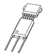
2. Pinning information
Table 1.
Pinning
Pin
Symbol
Description
1
VDD
supply voltage
2
GND
ground
3
OUT/DATA
analog output or data interface
Simplified outline
1
2
3
3. Ordering information
Table 2.
Ordering information
Type number
KMA199
KMA199
Product data sheet
Package
Name
Description
Version
-
plastic single-ended multi-chip package;
6 interconnections; 3 in-line leads
SOT880
All information provided in this document is subject to legal disclaimers.
Rev. 2 — 7 December 2011
© NXP B.V. 2011. All rights reserved.
2 of 36
�xxxx xxxxxxxxxxxxxxxxxxxxxxxxxxxxxx x xxxxxxxxxxxxxx xxxxxxxxxx xxx xxxxxx xxxxxxxxxxxxxxxxxxxxxxx xxxxxxxxxxxxxxxxxxxxxx
xxxxx xxxxxx xx xxxxxxxxxxxxxxxxxxxxxxxxxxxxx xxxxxxxxxxxxxxxxxxxxxx xxxxxxxxxxx xxxxxxx xxxxxxxxxxxxxxxxxxx
xxxxxxxxxxxxxxxx xxxxxxxxxxxxxx xxxxxx xx xxxxxxxxxxxxxxxxxxxxxxxxxxxxxxxx xxxxxxxxxxxxxxxxxxxxxxxx xxxxxxx
xxxxxxxxxxxxxxxxxxxxxxxxxxxxxxxxxxxxxxxxxxxxxx xxxxxxxxxxx xxxxx x x
VDDS
VDDS
REGULATOR
VDDA
REGULATOR
VDDD
REGULATOR
LOGIC
VDD
POWER-ON
RESET
NXP Semiconductors
Vref
Iref
4. Functional diagram
KMA199
Product data sheet
VDDE
VSSE
VSSE
Rev. 2 — 7 December 2011
All information provided in this document is subject to legal disclaimers.
POWER
LOST
Cblock
VSINP
MUX
AMPLIFIER
VSINN
2
2
VCOSP
A
D
D
A
OUTPUT
BUFFER
VO
OUT/
DATA
VCOSN
VSSS
TP0
TP1
TEST CONTROL
Q_PUMP
POWER
LOST
TP2
ARRAY
EEPROM
DIGITAL FILTER
OFFSET
AND
CORRECTION
AVERAGING
CORDIC
ALGORITHM
OFFSET
CALCULATION
ANGULAR
RANGE
ADJUSTMENT
ONE-WIRE
INTERFACE
OSC
DIGITAL BLOCKS (LOGIC)
VSSE
magnetoresistive
sensor bridges
008aaa233
KMA199
Functional diagram of KMA199
internal
protection
diodes
Programmable angle sensor
3 of 36
© NXP B.V. 2011. All rights reserved.
Fig 1.
signal conditioning integrated circuit
GND
�KMA199
NXP Semiconductors
Programmable angle sensor
5. Functional description
The KMA199 amplifies two orthogonal differential signals which are delivered by MR
sensor bridges and converts them into the digital domain. The angle is calculated using
the COordinate Rotation DIgital Computer (CORDIC) algorithm. After a digital-to-analog
conversion the analog signal is provided to the output. Thus, the output is a linear
representation of the angular value. Zero angle, clamping voltages and angular range are
programmable. In addition, two 16-bit registers are available for customer purposes, like
sample identification.
The KMA199 comprises a Cyclic Redundancy Check (CRC) and an Error Detection and
Correction (EDC) supervision, as well as a magnet-loss detection to ensure a fail-safe
operation. A power-loss detection circuit pulls the analog output to the remaining supply
line, if either the supply voltage or the ground line is interrupted.
After multiplexing the two MR Wheatstone bridge signals and their successive
amplification, the signal is converted into the digital domain by an Analog-to-Digital
Converter (ADC). Further processing is done within an on-chip state machine. This
includes offset cancellation, calculation of the mechanical angle using the CORDIC
algorithm, as well as zero angle and angular range adjustment. The internal
Digital-to-Analog Converter (DAC) and the analog output stage are used for conversion of
the angle information into an analog output voltage, which is ratiometric to the supply
voltage.
The configuration parameters are stored in an user-programmable EEPROM. The OWI
(accessible using pin OUT/DATA) is used for accessing the memory.
5.1 Angular measurement directions
The differential signals of the MR sensor bridges depend only on the direction of the
external magnetic field strength Hext, which is applied parallel to the plane of the sensor.
In order to obtain a correct output signal, the minimum saturation field strength has to be
exceeded.
KMA199
Product data sheet
All information provided in this document is subject to legal disclaimers.
Rev. 2 — 7 December 2011
© NXP B.V. 2011. All rights reserved.
4 of 36
�KMA199
NXP Semiconductors
Programmable angle sensor
α
Hext
001aag741
Fig 2.
Angular measurement directions
Since the Anisotropic MR (AMR) effect is periodic over 180, the sensor output is also
180-periodic, where the angle is calculated relative to a freely programmable zero angle.
The dashed line indicates the mechanical zero degree position.
6. Analog output
The KMA199 provides one analog output signal on pin OUT/DATA. The measured angle
is converted linearly into a value, which is ratiometric to the supply voltage VDD. Either a
positive or a negative slope is provided for this purpose.
The following table describes the analog output behavior for a positive slope. If for
example, a magnetic field angle, above the programmed maximum angle max, but below
the clamp switch angle sw(CL) is applied to the sensor, then analog output is set to the
upper clamping voltage. If the magnetic field angle is larger than the clamp switch angle,
the analog output switches from upper to lower clamping voltage. In the case of a
negative slope, the clamping voltages are changed.
Table 3.
Analog output behavior for a positive slope
Magnetic field angle
Analog output
max < < sw(CL)
V(CL)u
sw(CL) < < ref + 180
V(CL)l
The analog output voltage range codes both angular and diagnostic information. A valid
angle value is between the upper and lower clamping voltage. If the analog output is in the
diagnostic range, that is below 4 %VDD or above 96 %VDD, an error condition has been
detected. The analog output repeats every 180.
KMA199
Product data sheet
All information provided in this document is subject to legal disclaimers.
Rev. 2 — 7 December 2011
© NXP B.V. 2011. All rights reserved.
5 of 36
�KMA199
NXP Semiconductors
Programmable angle sensor
VO
(%VDD)
αrng
V(CL)u
V(CL)I
0
αref
α (deg)
αmax
180
αsw(CL)
αref + 180°
001aag811
max = ref + rng
Fig 3.
Characteristic of the analog output
7. Diagnostic features
The KMA199 provides four diagnostic features:
7.1 EEPROM CRC and EDC supervision
The KMA199 system includes a supervision of the programmed data. At power-on, a CRC
of the EEPROM is performed. Furthermore the EEPROM is protected against bit errors.
Every 16-bit data word is saved internally as a 22-bit word for this purpose. The protection
logic corrects any single-bit error in a data word, while the sensor continues in normal
operation mode. Multiple bit errors per word will be detected and switches the device into
diagnostic mode.
7.2 Magnet-loss detection
If the applied magnetic field strength is not sufficient, the KMA199 raises a diagnostic
condition. In order to enter the diagnostic mode, due to EEPROM CRC or magnet-loss
detection, the device can be programmed into active diagnostic mode, where the output is
driven below 4 %VDD or above 96 %VDD.
7.3 Power-loss detection
The power-loss detection circuits enable the detection of an interrupted supply or ground
line of the KMA199. In the case of a power-loss condition, two internal switches in sensor
are closed, connecting the pin of the analog output with the supply voltage and the ground
pins.
KMA199
Product data sheet
All information provided in this document is subject to legal disclaimers.
Rev. 2 — 7 December 2011
© NXP B.V. 2011. All rights reserved.
6 of 36
�KMA199
NXP Semiconductors
Programmable angle sensor
KMA199
VDD
ZO(pl)
OUT/DATA
ZO(pl)
GND
008aaa234
Fig 4. Equivalent output circuit in case of a power-loss condition
Table 4 shows the resulting output voltage depending on the error case and the load
resistance.
Table 4.
Power-loss behavior
Load resistance
Supply voltage lost
Ground lost
RL > 5 k
VO 4 %VDD
VO 96 %VDD
7.4 Low supply voltage detection
If the supply voltage is below the switch-off threshold voltage, a status bit is set.
Table 5 describes the behavior of the analog output at different supply voltages.
Table 5.
Supply voltage behavior
Voltage range
Description
Analog output
0 V to 1.5 V
the output drives an active LOW, but the
switches of the power-loss detection circuits
are not fully opened and set the output to a
level between ground and half the supply
voltage
actively driven output to a
voltage level between ground
and half the supply voltage
1.5 V to VPOR
all modules begin to work and the power-on
reset is active
diagnostics at LOW level
VPOR to Vth(on) or
Vth(off)
all modules begin to work and the digital part is EEPROM defined diagnostic
initialized
level
Vth(on) or Vth(off) to analog output is switched on after power-on
4.5 V
time and represents the measured angle
4.5 V to 5.5 V
KMA199
Product data sheet
analog output of the
measured angle without the
specified accuracy
normal operation where the sensor works with analog output of the
the specified accuracy
measured angle
All information provided in this document is subject to legal disclaimers.
Rev. 2 — 7 December 2011
© NXP B.V. 2011. All rights reserved.
7 of 36
�KMA199
NXP Semiconductors
Programmable angle sensor
8. Limiting values
Table 6.
Limiting values
In accordance with the Absolute Maximum Rating System (IEC 60134).
Symbol
Parameter
VDD
supply voltage
Conditions
tinit < 200 h
Min
Max
Unit
0.3
+5.7
V
V
[1]
-
6.0
[2]
0.3
VDD + 0.3 V
-
150
mA
VO
output voltage
Ir
reverse current
Tamb
ambient temperature
40
+160
C
Tamb(pr)
programming ambient temperature
10
70
C
Tstg
storage temperature
40
+125
C
Tamb = 50 C
17
-
year
Tamb(pr) = 70 C
100
-
cycle
Min
Typ
Max
Unit
4.5
5.0
5.5
V
40
-
+160 C
Tamb < 70 C
EEPROM
tret(D)
data retention time
Nendu(W_ER) write or erase endurance
[1]
Time until sensor environment is initialized.
[2]
The maximum value of the output voltage is 5.7 V.
9. Recommended operating conditions
Table 7.
Operating conditions
In a homogenous magnetic field.
Symbol
Parameter
VDD
supply voltage
Tamb
ambient temperature
Conditions
[1]
Tamb(pr)
programming ambient temperature
10
-
70
C
CL
load capacitance
[2]
0
-
22
nF
Cblock
blocking capacitance
[3]
75
-
nF
RL
load resistance
[4]
5
-
k
Hext
external magnetic field strength
35
-
-
kA/m
[1]
Normal operating mode.
[2]
Between ground and analog output, as close as possible to the package for improved electromagnetic
immunity.
[3]
Between ground and supply voltage, as close as possible to the package and with a low equivalent series
resistance.
[4]
Power-loss detection is only possible with a load resistance within the specified range connected to the
supply or ground line.
10. Thermal characteristics
Table 8.
KMA199
Product data sheet
Thermal characteristics
Symbol
Parameter
Rth(j-a)
thermal resistance from junction to
ambient
Conditions
All information provided in this document is subject to legal disclaimers.
Rev. 2 — 7 December 2011
Typ
Unit
120
K/W
© NXP B.V. 2011. All rights reserved.
8 of 36
�KMA199
NXP Semiconductors
Programmable angle sensor
11. Characteristics
Table 9.
Supply current
Characteristics are valid for the operating conditions, as specified in Section 9.
Symbol
Parameter
Conditions
[1][2]
supply current
IDD
[1]
Normal operating mode.
[2]
Without load current at the analog output.
Min
Typ
Max
Unit
5
-
10
mA
Table 10. Power-on reset
Characteristics are valid for the operating conditions, as specified in Section 9.
Symbol
Parameter
Conditions
Min
Typ
Max
Unit
Vth(on)
switch-on threshold
voltage
analog output switches on, if
VDD > Vth(on)
4.00
4.30
4.45
V
Vth(off)
switch-off threshold
voltage
analog output switches off, if
VDD < Vth(off)
-
4.20
4.30
V
Vhys
hysteresis voltage
Vhys = Vth(on) Vth(off)
0.1
-
0.4
V
VPOR
power-on reset voltage
IC is initialized
2.4
-
3.3
V
Table 11. System performance
Characteristics are valid for the operating conditions, as specified in Section 9.
Symbol
Parameter
Conditions
Min
Typ
Max
Unit
[1]
res
angle resolution
-
-
0.04
deg
max
maximum angle
programmable angular range
for V(CL)u V(CL)l 80 %VDD
[2]
5
-
180
deg
ref
reference angle
programmable zero angle
[2]
0
-
180
deg
VO(nom)
nominal output voltage
at full supply operating range
5
-
95
%VDD
VO(udr)
upper diagnostic range
output voltage
[3]
96
-
100
%VDD
VO(ldr)
lower diagnostic range
output voltage
[3]
0
-
4
%VDD
V(CL)u
upper clamping voltage
[4]
40
-
95
%VDD
V(CL)l
lower clamping voltage
[4]
5
-
30.5
%VDD
V(CL)
clamping voltage variation
deviation from programmed
value
0.3
-
+0.3
%VDD
IO
output current
normal operation mode;
operating as sink or source
-
-
2
mA
Vn(o)(RMS)
RMS output noise voltage
equivalent power noise
lin
temp
linearity error
temperature drift error
KMA199
Product data sheet
[5]
-
0.4
2.5
mV
temperature range
40 C to +160 C
[5][6]
1.2
-
+1.2
deg
temperature range
40 C to +140 C
[5][6]
1
-
+1
deg
temperature range
40 C to +160 C
[1][5][6]
-
-
0.8
deg
temperature range
40 C to +140 C
[1][5][6]
-
-
0.65
deg
[7]
[7]
All information provided in this document is subject to legal disclaimers.
Rev. 2 — 7 December 2011
© NXP B.V. 2011. All rights reserved.
9 of 36
�KMA199
NXP Semiconductors
Programmable angle sensor
Table 11. System performance …continued
Characteristics are valid for the operating conditions, as specified in Section 9.
Symbol
tempRT
hys
lin
ang
Parameter
temperature drift error at
room temperature
hysteresis error
microlinearity error
angular error
mang
slope of angular error
ZO(pl)
power-loss output
impedance
Conditions
Min
Typ
Max
Unit
temperature range
40 C to +160 C
[6][7][8]
-
-
0.65
deg
temperature range
40 C to +140 C
[6][7][8]
-
-
0.55
deg
referred to input
[5][6]
-
-
0.09
deg
referred to input
[5][6]
0.1
-
+0.1
deg
temperature range
40 C to +160 C
[5][6][9]
1.35
-
+1.35
deg
temperature range
40 C to +140 C
[5][6][9]
1.1
-
+1.1
deg
[5][6][9]
-
-
0.04
deg/deg
-
-
210
impedance to remaining
supply line in case of lost
supply voltage or lost ground
[1]
At a nominal output voltage between 5 %VDD and 95 %VDD and a maximum angle of max = 180.
[2]
In steps of resolution < 0.022.
[3]
Activation is dependent on the programmed diagnostic mode.
[4]
In steps of 0.02 %VDD.
[5]
At a low-pass filtered analog output with a cut-off frequency of 0.7 kHz.
[6]
Definition of errors is given in Section 12.
[7]
Based on a 3 standard deviation.
[8]
Room temperature is given for an ambient temperature of 25 C.
[9]
Graph of angular error is shown in Figure 5.
KMA199
Product data sheet
All information provided in this document is subject to legal disclaimers.
Rev. 2 — 7 December 2011
© NXP B.V. 2011. All rights reserved.
10 of 36
�KMA199
NXP Semiconductors
Programmable angle sensor
1.40
1.35
|Δφang|
(deg)
1.10
(1)
(2)
0.75
0.65
0
−20
−16
−12.25
−1 0 1
12.25
20
16
α1 − α0 (deg)
001aal765
(1) 40 C to +160 C.
(2) 40 C to +140 C.
Fig 5.
Envelope curve for the magnitude of angular error
Table 12. Dynamics
Characteristics are valid for the operating conditions, as specified in Section 9.
Symbol
Parameter
Conditions
ton
turn-on time
fupd
update frequency
ts
settling time
tcmd(ent)
enter command mode time after power on
[1]
until first valid result
after an ideal mechanical
angle step of 45, until 90 %
of the final value is reached;
CL = 5 nF
Min
[1]
Typ
Max
Unit
-
-
5
ms
2
3.125
-
kHz
-
-
1.8
ms
16
-
26
ms
Min
Typ
Max
Unit
After reaching the power-on threshold voltage.
Table 13. Digital interface
Characteristics are valid for the operating conditions, as specified in Section 9.
Symbol
Parameter
VIH
HIGH-level input voltage
80
-
-
%VDD
VIL
LOW-level input voltage
-
-
20
%VDD
VOH
HIGH-level output voltage
IO = 2 mA
80
-
-
%VDD
VOL
LOW-level output voltage
IO = 2 mA
-
-
20
%VDD
Iod
overdrive current
absolute value for overdriving
the output buffer
-
-
20
mA
tstart
start time
LOW level before rising edge
5
-
-
s
KMA199
Product data sheet
Conditions
All information provided in this document is subject to legal disclaimers.
Rev. 2 — 7 December 2011
© NXP B.V. 2011. All rights reserved.
11 of 36
�KMA199
NXP Semiconductors
Programmable angle sensor
Table 13. Digital interface …continued
Characteristics are valid for the operating conditions, as specified in Section 9.
Symbol
Parameter
Conditions
Min
Typ
Max
Unit
tstop
stop time
HIGH level before falling edge
5
-
-
s
Tbit
bit period
minimum period may be
limited by the load
capacitance
10
-
100
s
Tbit
bit period deviation
deviation between received
clock and sent clock
0.8Tbit
1Tbit
1.2Tbit
s
tw0
pulse width 0
0.175Tbit
0.25Tbit
0.375Tbit
s
tw1
pulse width 1
0.625Tbit
0.75Tbit
0.825Tbit
s
tto
time-out time
digital communication reset
guaranteed after maximum tto
-
-
220
s
ttko(slv)
slave takeover time
duration of LOW level for
slave takeover
1
-
5
s
ttko(mas)
master takeover time
duration of LOW level for
master takeover
0Tbit
-
0.5Tbit
s
tprog
programming time
for a single EEPROM address
20
-
-
ms
tcp
charge pump time
waiting time after enabling the
EEPROM charge pump clock
1
-
-
ms
12. Definition of errors
12.1 General
Angular measurement errors by the KMA199 result from linearity errors, temperature drift
errors and hysteresis errors. Figure 6 shows the output signal of an ideal sensor, where
the measured angle meas corresponds ideally to the magnetic field angle . This curve
will further be denoted as angle reference line ref() with a slope of 0.5 %VDD/deg.
φmeas
(deg)
φref(α)
180
α (deg)
001aag812
Fig 6. Definition of the reference line
The angular range is set to max = 180 and the clamping voltages are programmed to
V(CL)l = 5 %VDD and V(CL)u = 95 %VDD for a valid definition of errors.
KMA199
Product data sheet
All information provided in this document is subject to legal disclaimers.
Rev. 2 — 7 December 2011
© NXP B.V. 2011. All rights reserved.
12 of 36
�KMA199
NXP Semiconductors
Programmable angle sensor
12.2 Hysteresis error
The hysteresis error hys is defined as the maximum difference between the angles,
given by the device output when performing a positive (clockwise) rotation and negative
(counter clockwise) rotation over an angular range of 180, measured at a constant
temperature.
φmeas
(deg)
Δφhys
180
α (deg)
001aag813
Fig 7. Definition of the hysteresis error
Equation 1 gives the mathematical description for the hysteresis value hys:
hys() = meas( 180 ) – meas( 0 )
(1)
12.3 Linearity error
The KMA199 output signal deviation from a best straight line BSL, with the same slope as
the reference line, is defined as linearity error. The magnetic field angle is varied at fixed
temperatures for measurement of this linearity error. The output signal deviation from the
best straight line at the given temperature is the linearity error lin. It is a function of the
magnetic field angle and the temperature of the device Tamb.
φmeas
(deg)
φBSL(α, Tamb)
φref(α)
Δφlin(α, Tamb)
180
α (deg)
001aag814
Fig 8. Definition of the linearity error
KMA199
Product data sheet
All information provided in this document is subject to legal disclaimers.
Rev. 2 — 7 December 2011
© NXP B.V. 2011. All rights reserved.
13 of 36
�KMA199
NXP Semiconductors
Programmable angle sensor
12.4 Microlinearity error
The microlinearity error lin is the device output deviation from 1, if the magnetic field
angle is changed by = 1.
φmeas
(deg)
φref(α)
Δφmeas = 1° + Δφμlin(α)
Δα = 1°
α (deg)
001aag815
Fig 9. Definition of the microlinearity error
12.5 Temperature drift error
The temperature drift temp is defined as the envelope over the deviation of the angle
versus the temperature range. It is considered as the pure thermal effect.
φmeas
(deg)
Ty
Tx
Δφtemp
180
α (deg)
001aag816
Fig 10. Definition of the temperature drift error
Equation 2 gives the mathematical description for temperature drift value temp:
temp() = meas( , T x) – meas( , T y)
(2)
with:
Tx: temperature for maximum meas at angle
Ty: temperature for minimum meas at angle
KMA199
Product data sheet
All information provided in this document is subject to legal disclaimers.
Rev. 2 — 7 December 2011
© NXP B.V. 2011. All rights reserved.
14 of 36
�KMA199
NXP Semiconductors
Programmable angle sensor
The deviation from the value at room temperature tempRT describes the temperature
drift of the angle, compared to the value, which the sensor provides at room temperature:
temp
RT( ,
T amb) = meas( , T amb) – meas( , T RT)
(3)
with:
TRT: room temperature (25 C)
12.6 Angular error
The angular error ang is the error of angle difference measured by the sensor, if the
mechanical angle deviates from 0 to 1. Here 0 and 1 are arbitrary angles within the
angular range. The angle measurement at 0 is the initially programmed reference angle,
programmed by the customer at room temperature and zero hour upon production. The
angle measurement at 1 is made at any temperature within the ambient temperature
range:
ang = meas( 1 , T amb) – meas( 0 , T RT) – 1 – 0
(4)
with:
0, 1: arbitrary mechanical angles within the angular range
meas(0, TRT): programmed angle at 0, TRT = 25 C and zero hour upon production
meas(1, Tamb): angle measured by the sensor at 1 and any temperature within Tamb
This error comprises non-linearity and temperature drift related to the room temperature.
|Δφang|
mang
|Δφang(peak)|
|Δφμlin + Δφtemp|RT|
−α*
α0 − 1° α0 + 1°
α0
+α*
α1
001aal766
Fig 11. Definition of the angular error
Figure 11 shows the envelope curve for the magnitude of angular error |ang| versus 1
for all angles 0 and all temperatures Tamb within the ambient temperature range. |ang|
has its minimum, if 1 is in the range of 1 around 0. Here only the microlinearity error
lin and the temperature drift related to the room temperature |tempRT| occurs. If 1
deviates from 0 by more than 1 in either direction, |ang| can increase with a gradient
defined by slope mang.
KMA199
Product data sheet
All information provided in this document is subject to legal disclaimers.
Rev. 2 — 7 December 2011
© NXP B.V. 2011. All rights reserved.
15 of 36
�KMA199
NXP Semiconductors
Programmable angle sensor
Angular error can be expressed by Equation 5 to Equation 8:
for |1 0| 1
ang = lin + temp
(5)
RT
for 1 < |1 0| < *
ang = lin + temp
RT
+ m ang 1 – 0 – 1
(6)
RT
(7)
for |1 0| *
ang =
lin 2 + temp
2
with:
ang(peak) – lin + temp RT
= ----------------------------------------------------------------------------------- + 0 + 1
m ang
(8)
13. Programming
13.1 General description
The KMA199 provides an OWI to enable programming of the device which uses
pin OUT/DATA bidirectionally.
In general the device runs in analog output mode, the normal operating mode. This mode
is configured by the embedded programming data and is started after a power-on reset
once time ton has elapsed. In this mode, the magnetic field angle is converted into the
corresponding output voltage.
Command mode has to be entered to enable programming. In this mode, the customer
can adjust all required parameters (for example zero angle and angular range) to meet the
application requirements. After enabling the internal charge pump and waiting for tcp the
data is stored in the EEPROM. After changing the contents of the EEPROM, the
checksum must be recalculated and written (see Section 13.4).
In order to enter the command mode, a specific command sequence must be send after a
power-on reset and during the time slot tcmd(ent). The external source used to send the
command sequence must overdrive the output buffer of the KMA199 (I > Iod).
KMA199
Product data sheet
All information provided in this document is subject to legal disclaimers.
Rev. 2 — 7 December 2011
© NXP B.V. 2011. All rights reserved.
16 of 36
�KMA199
NXP Semiconductors
Programmable angle sensor
During communication, the KMA199 is always the slave and the external programming
hardware is the master. Figure 12 illustrates the structure of the OWI data format.
write
IDLE
START COMMAND DATA BYTE 1 DATA BYTE 2 STOP
IDLE
read
IDLE
START COMMAND HANDOVER DATA BYTE 1 DATA BYTE 2 TAKEOVER STOP IDLE
001aag742
Fig 12. OWI data format
The master provides the start condition, which is a rising edge after a LOW level. Then a
command byte which can be either a read or a write command is send. Depending on the
command, the master or the slave has to send the data immediately after the command
sequence. In the case of a read command, an additional handover or takeover bit is
inserted before and after the data bytes. Each communication must be closed with a stop
condition driven by the master. If the slave does not receive a rising edge for a time longer
than tto, a time-out condition occurs. The bus is reset to the idle state and waits for a start
condition and a new command. This can be used to synchronize the device regardless of
the previous state.
All communication is based on this structure (see Figure 12), even for entering the
command mode. In this case a special write command is required, followed by the
command sequence (two data bytes). The customer can access the EEPROM, CTRL1,
TESTCTRL0 and SIGNATURE registers (described in Section 13.5). Only a power-on
reset will leave the command mode. A more detailed description of the programming is
given in the next sections.
13.2 Timing characteristics
As described in the previous section, a start and stop condition is necessary for
communication. The LOW-level duration before the rising edge of the start condition is
defined as tstart. The HIGH-level duration after the rising edge of the stop condition is
defined as tstop. These parameters, together with all other timing characteristics are
shown in Table 13.
tstart
tstop
001aag817
Fig 13. OWI start and stop condition
KMA199
Product data sheet
All information provided in this document is subject to legal disclaimers.
Rev. 2 — 7 December 2011
© NXP B.V. 2011. All rights reserved.
17 of 36
�KMA199
NXP Semiconductors
Programmable angle sensor
Figure 14 shows the coding of a single bit with a HIGH level of VIH and a LOW level of VIL.
Here the pulse width t1 or t0 represents a logic 1 or a logic 0 of a full bit period Tbit,
respectively.
bit = 0
bit = 1
Tbit
0.175
Tbit
0.375
0.625
tw0
0.825
tw1
0.25
0.75
001aag818
Fig 14. OWI timing
13.3 Sending and receiving data
The master has to control the communication during sending or receiving data.
The command byte defines the region, address and type of command requested by the
master. In case of a read command, an additional handover or takeover bit must be
inserted before and after the two data bytes (see Figure 12). However the OWI is a serial
data transmission, whereas the Most Significant Byte (MSB) must be send at first.
Table 14.
Format of a command byte
7
6
5
4
3
2
1
0
CMD7
CMD6
CMD5
CMD4
CMD3
CMD2
CMD1
CMD0
Table 15.
Command byte bit description
Bit
Symbol
Description
7 to 5
CMD[7:5]
region bits
000 = 16-bit EEPROM
001 to 011 = reserved
100 = 16-bit register
101 to 111 = reserved
4 to 1
CMD[4:1]
address bits
0
CMD0
read/write
0 = write
1 = read
A more detailed description of all customer accessible registers is given in Section 13.5.
Both default value and the complete command including the address and write or read
request are also listed.
KMA199
Product data sheet
All information provided in this document is subject to legal disclaimers.
Rev. 2 — 7 December 2011
© NXP B.V. 2011. All rights reserved.
18 of 36
�KMA199
NXP Semiconductors
Programmable angle sensor
13.3.1 Write access
To write data to the EEPROM, the internal charge pump must be enabled by setting the
bits EEP_CP_CLOCK_EN and EEP_WRITE_EN and waiting for tcp. The following
procedure must be performed:
•
•
•
•
Start condition: The master drives a rising edge after a LOW level
Command: The master sends a write command (CMD0 = 0)
Data: The master sends two data bytes
Stop condition: The master drives a rising edge after a LOW level
Figure 15 shows the write access of the digital interface. The signal OWI represents the
data on the bus from the master or slave. The signals master output enable and slave
output enable just symbolize if the master or the slave output is enabled or disabled,
respectively.
START
CMD7
CMD0
WDATA15
WDATA0
STOP
IDLE
master
output
enable
OWI
(2)
slave
output
enable
(1)
001aag743
(1) Missing rising edges generate a time-out condition and the written data is ignored.
(2) If the master does not drive the bus, the bus is defined by the bus-pull.
Fig 15. OWI write access
Note: As already mentioned in Section 13.1, the command mode has to be entered using
the write procedure. If command mode is not entered, digital communication is not
possible and the sensor operates in normal operating mode. After changing an address,
the time tprog must elapse before changing another address. Finally the checksum must
be recalculated and written, after changing the contents of the EEPROM
(see Section 13.4).
KMA199
Product data sheet
All information provided in this document is subject to legal disclaimers.
Rev. 2 — 7 December 2011
© NXP B.V. 2011. All rights reserved.
19 of 36
�KMA199
NXP Semiconductors
Programmable angle sensor
13.3.2 Read access
To read data from the sensor, the following procedure must be performed:
• Start condition: The master drives a rising edge after a LOW level
• Command: The master sends a read command (CMD0 = 1)
• Handover: The master sends a handover bit, that is a logic 0 and disables the output
after a three-quarter bit period
• Takeover: The slave drives a LOW level after the falling edge for ttko(slv)
• Data: The slave sends two data bytes
• Handover: The slave sends a handover bit, that is a logic 0 and disables the output
after a three-quarter bit period
• Takeover: The master drives a LOW level after the falling edge for ttko(mas)
• Stop condition: The master drives a rising edge after a LOW level
Figure 16 shows the read access of the digital interface. The signal OWI represents the
data on the bus from the master or slave. The signals master output enable and slave
output enable just symbolize if the master or the slave output is enabled or disabled,
respectively.
START
CMD7
CMD0
HANDSHAKE
RDATA15
RDATA0
HANDSHAKE
STOP
IDLE
master
output
enable
(3)
OWI
(5)
(1)
slave
output
enable
(2)
(2)
(4)
001aag744
(1) Duration of LOW level for slave takeover ttko(slv).
(2) There is an overlap in the output enables of master and slave, because both drive a LOW level.
However this ensures the independency from having a pull-up or pull-down on the bus. In addition
it improves the ElectroMagnetic Compatibility (EMC) robustness, because all levels are actively
driven.
(3) Duration of LOW level for master takeover ttko(mas).
(4) If the master does not take over and a pull-up exists, the stop condition is generated by the pull-up.
Otherwise a time-out is generated if there is a pull-down and the slave waits for a rising edge as
start condition.
(5) If the master does not drive the bus, the bus is defined by the bus-pull.
Fig 16. OWI read access
KMA199
Product data sheet
All information provided in this document is subject to legal disclaimers.
Rev. 2 — 7 December 2011
© NXP B.V. 2011. All rights reserved.
20 of 36
�KMA199
NXP Semiconductors
Programmable angle sensor
13.3.3 Entering the command mode
After a power-on reset, the sensor provides a time slot tcmd(ent) for entering the command
mode. A specific command sequence has to be send (see Figure 17). If command mode
is not entered, the sensor starts in the normal operating mode. However the signature can
be written by the master, if the sensor switches to diagnostic mode.
During the command mode sequence, the analog output is enabled. The external
programming hardware has to overdrive the output with the current Iod. If command mode
is activated, the analog output is disabled and pin OUT/DATA operates as a digital
interface.
tcmd(ent)
VDD
OWI
START
94h
command
9Bh
A4h
STOP
signature
001aag819
Fig 17. OWI command mode procedure
13.4 Cyclic redundancy check
As already mentioned in Section 7, there is an 8-bit checksum for the EEPROM data.
To calculate this value, the CRC needs to be generated with the MSB of the EEPROM
data word at first over all corresponding addresses in increasing order.
All addresses from 0h to Fh have to be read out for calculating the checksum. The Least
Significant Byte (LSB) of address Fh which contains the previous checksum must be
overwritten with 0h before the calculation can be started.
Finally, the internal charge pump has to be enabled for programming by setting the bits
EEP_CP_CLOCK_EN and EEP_WRITE_EN (see Table 16) and waiting for tcp.
The generator polynomial for the calculation of the checksum is:
8
2
G(x) = x + x + x + 1
(9)
With a start value of FFh and the data bits are XOR at the x8 point.
KMA199
Product data sheet
All information provided in this document is subject to legal disclaimers.
Rev. 2 — 7 December 2011
© NXP B.V. 2011. All rights reserved.
21 of 36
�KMA199
NXP Semiconductors
Programmable angle sensor
13.4.1 Software example in C
1
2
3
4
5
6
7
8
9
10
11
12
13
14
15
16
17
18
19
20
21
22
23
24
25
26
27
28
29
30
31
32
33
34
35
36
37
38
39
40
41
42
43
#include
// calc_crc accepts unsigned 16-bit data in data
int calc_crc(int crc, unsigned int data)
{
const int gpoly = 0x107; // generator polynomial
int i;
//index variable
for (i = 15; i >= 0; i--)
{
crc


 工商网监
湘ICP备2023018690号
工商网监
湘ICP备2023018690号
