Freescale Semiconductor
Document Number: MPC875EC
Rev. 4, 08/2007
Technical Data
MPC875/MPC870 PowerQUICC™
Hardware Specifications
This hardware specification contains detailed information on
power considerations, DC/AC electrical characteristics, and
AC timing specifications for the MPC875/MPC870. The
CPU on the MPC875/MPC870 is a 32-bit core built on
Power Architecture™ technology that incorporates memory
management units (MMUs) and instruction and data caches.
For functional characteristics of the MPC875/MPC870, refer
to the MPC885 PowerQUICC™ Family Reference Manual.
To locate published errata or updates for this document, refer
to the MPC875/MPC870 product summary page on our
website listed on the back cover of this document or, contact
your local Freescale sales office.
© Freescale Semiconductor, Inc., 2003–2007. All rights reserved.
1.
2.
3.
4.
5.
6.
7.
8.
9.
10.
11.
12.
13.
14.
15.
16.
17.
Contents
Overview . . . . . . . . . . . . . . . . . . . . . . . . . . . . . . . . . . . 2
Features . . . . . . . . . . . . . . . . . . . . . . . . . . . . . . . . . . . . 2
Maximum Tolerated Ratings . . . . . . . . . . . . . . . . . . . 9
Thermal Characteristics . . . . . . . . . . . . . . . . . . . . . . 10
Power Dissipation . . . . . . . . . . . . . . . . . . . . . . . . . . . 11
DC Characteristics . . . . . . . . . . . . . . . . . . . . . . . . . . 11
Thermal Calculation and Measurement . . . . . . . . . . 12
Power Supply and Power Sequencing . . . . . . . . . . . 14
Mandatory Reset Configurations . . . . . . . . . . . . . . . 15
Layout Practices . . . . . . . . . . . . . . . . . . . . . . . . . . . . 16
Bus Signal Timing . . . . . . . . . . . . . . . . . . . . . . . . . . 17
IEEE 1149.1 Electrical Specifications . . . . . . . . . . . 45
CPM Electrical Characteristics . . . . . . . . . . . . . . . . . 47
USB Electrical Characteristics . . . . . . . . . . . . . . . . . 67
FEC Electrical Characteristics . . . . . . . . . . . . . . . . . 67
Mechanical Data and Ordering Information . . . . . . . 71
Document Revision History . . . . . . . . . . . . . . . . . . . 80
�Overview
1
Overview
The MPC875/MPC870 is a versatile single-chip integrated microprocessor and peripheral combination
that can be used in a variety of controller applications and communications and networking systems. The
MPC875/MPC870 provides enhanced ATM functionality over that of other ATM-enabled members of the
MPC860 family.
Table 1 shows the functionality supported by the MPC875/MPC870.
Table 1. MPC875/MPC870 Devices
Cache (Kbytes)
Ethernet
Part
2
SCC
SMC
USB
Security
Engine
I Cache
D Cache
10BaseT
10/100
MPC875
8
8
1
2
1
1
1
Yes
MPC870
8
8
—
2
—
1
1
No
Features
The MPC875/MPC870 is comprised of three modules that each use the 32-bit internal bus: a MPC8xx
core, a system integration unit (SIU), and a communications processor module (CPM).
The following list summarizes the key MPC875/MPC870 features:
• Embedded MPC8xx core up to 133 MHz
• Maximum frequency operation of the external bus is 80 MHz (in 1:1 mode)
— The 133-MHz core frequency supports 2:1 mode only
— The 66-/80-MHz core frequencies support both the 1:1 and 2:1 modes
• Single-issue, 32-bit core (compatible with the Power Architecture definition) with thirty-two
32-bit general-purpose registers (GPRs)
— The core performs branch prediction with conditional prefetch and without conditional
execution
— 8-Kbyte data cache and 8-Kbyte instruction cache (see Table 1)
– Instruction cache is two-way, set-associative with 256 sets in 2 blocks
– Data cache is two-way, set-associative with 256 sets
– Cache coherency for both instruction and data caches is maintained on 128-bit (4-word)
cache blocks
– Caches are physically addressed, implement a least recently used (LRU) replacement
algorithm, and are lockable on a cache block basis
— MMUs with 32-entry TLB, fully associative instruction and data TLBs
— MMUs support multiple page sizes of 4, 16, and 512 Kbytes, and 8 Mbytes; 16 virtual address
spaces and 16 protection groups
— Advanced on-chip emulation debug mode
• Up to 32-bit data bus (dynamic bus sizing for 8, 16, and 32 bits)
MPC875/MPC870 PowerQUICC™ Hardware Specifications, Rev. 4
2
Freescale Semiconductor
�Features
•
•
•
•
•
•
Thirty-two address lines
Memory controller (eight banks)
— Contains complete dynamic RAM (DRAM) controller
— Each bank can be a chip select or RAS to support a DRAM bank
— Up to 30 wait states programmable per memory bank
— Glueless interface to DRAM, SIMMS, SRAM, EPROMs, Flash EPROMs, and other memory
devices
— DRAM controller programmable to support most size and speed memory interfaces
— Four CAS lines, four WE lines, and one OE line
— Boot chip-select available at reset (options for 8-, 16-, or 32-bit memory)
— Variable block sizes (32 Kbytes–256 Mbytes)
— Selectable write protection
— On-chip bus arbitration logic
General-purpose timers
— Four 16-bit timers or two 32-bit timers
— Gate mode can enable/disable counting
— Interrupt can be masked on reference match and event capture
Two Fast Ethernet controllers (FEC)—Two 10/100 Mbps Ethernet/IEEE Std. 802.3® CDMA/CS
that interface through MII and/or RMII interfaces
System integration unit (SIU)
— Bus monitor
— Software watchdog
— Periodic interrupt timer (PIT)
— Clock synthesizer
— Decrementer and time base
— Reset controller
— IEEE 1149.1™ Std. test access port (JTAG)
Security engine is optimized to handle all the algorithms associated with IPsec, SSL/TLS, SRTP,
IEEE 802.11i® standard, and iSCSI processing. Available on the MPC875, the security engine
contains a crypto-channel, a controller, and a set of crypto hardware accelerators (CHAs). The
CHAs are:
— Data encryption standard execution unit (DEU)
– DES, 3DES
– Two key (K1, K2, K1) or three key (K1, K2, K3)
– ECB and CBC modes for both DES and 3DES
— Advanced encryption standard unit (AESU)
– Implements the Rijndael symmetric key cipher
MPC875/MPC870 PowerQUICC™ Hardware Specifications, Rev. 4
Freescale Semiconductor
3
�Features
•
•
•
•
•
– ECB, CBC, and counter modes
– 128-, 192-, and 256-bit key lengths
— Message digest execution unit (MDEU)
– SHA with 160- or 256-bit message digest
– MD5 with 128-bit message digest
– HMAC with either algorithm
— Master/slave logic, with DMA
– 32-bit address/32-bit data
– Operation at MPC8xx bus frequency
— Crypto-channel supporting multi-command descriptors
– Integrated controller managing crypto-execution units
– Buffer size of 256 bytes for each execution unit, with flow control for large data sizes
Interrupts
— Six external interrupt request (IRQ) lines
— Twelve port pins with interrupt capability
— Twenty-three internal interrupt sources
— Programmable priority between SCCs
— Programmable highest priority request
Communications processor module (CPM)
— RISC controller
— Communication-specific commands (for example, GRACEFUL STOP TRANSMIT, ENTER HUNT
MODE, and RESTART TRANSMIT)
— Supports continuous mode transmission and reception on all serial channels
— 8-Kbytes of dual-port RAM
— Several serial DMA (SDMA) channels to support the CPM
— Three parallel I/O registers with open-drain capability
On-chip 16 × 16 multiply accumulate controller (MAC)
— One operation per clock (two-clock latency, one-clock blockage)
— MAC operates concurrently with other instructions
— FIR loop—Four clocks per four multiplies
Four baud-rate generators
— Independent (can be connected to SCC or SMC)
— Allows changes during operation
— Autobaud support option
SCC (serial communication controller)
— Ethernet/IEEE 802.3® standard, supporting full 10-Mbps operation
— HDLC/SDLC
MPC875/MPC870 PowerQUICC™ Hardware Specifications, Rev. 4
4
Freescale Semiconductor
�Features
•
•
•
•
— HDLC bus (implements an HDLC-based local area network (LAN))
— Asynchronous HDLC to support point-to-point protocol (PPP)
— AppleTalk
— Universal asynchronous receiver transmitter (UART)
— Synchronous UART
— Serial infrared (IrDA)
— Binary synchronous communication (BISYNC)
— Totally transparent (bit streams)
— Totally transparent (frame based with optional cyclic redundancy check (CRC))
SMC (serial management channel)
— UART (low-speed operation)
— Transparent
Universal serial bus (USB)—Supports operation as a USB function endpoint, a USB host
controller, or both for testing purposes (loopback diagnostics)
— USB 2.0 full-/low-speed compatible
— The USB function mode has the following features:
– Four independent endpoints support control, bulk, interrupt, and isochronous data transfers
– CRC16 generation and checking
– CRC5 checking
– NRZI encoding/decoding with bit stuffing
– 12- or 1.5-Mbps data rate
– Flexible data buffers with multiple buffers per frame
– Automatic retransmission upon transmit error
— The USB host controller has the following features:
– Supports control, bulk, interrupt, and isochronous data transfers
– CRC16 generation and checking
– NRZI encoding/decoding with bit stuffing
– Supports both 12- and 1.5-Mbps data rates (automatic generation of preamble token and
data rate configuration). Note that low-speed operation requires an external hub.
– Flexible data buffers with multiple buffers per frame
– Supports local loopback mode for diagnostics (12 Mbps only)
Serial peripheral interface (SPI)
— Supports master and slave modes
— Supports multiple-master operation on the same bus
Inter-integrated circuit (I2C) port
— Supports master and slave modes
— Supports a multiple-master environment
MPC875/MPC870 PowerQUICC™ Hardware Specifications, Rev. 4
Freescale Semiconductor
5
�Features
•
•
•
•
•
•
The MPC875 has a time-slot assigner (TSA) that supports one TDM bus (TDMb)
— Allows SCC and SMC to run in multiplexed and/or non-multiplexed operation
— Supports T1, CEPT, PCM highway, ISDN basic rate, ISDN primary rate, user-defined
— 1- or 8-bit resolution
— Allows independent transmit and receive routing, frame synchronization, and clocking
— Allows dynamic changes
— Can be internally connected to two serial channels (one SCC and one SMC)
PCMCIA interface
— Master (socket) interface, release 2.1-compliant
— Supports one independent PCMCIA socket on the MPC875/MPC870
— Eight memory or I/O windows supported
Debug interface
— Eight comparators: four operate on instruction address, two operate on data address, and two
operate on data
— Supports conditions: = ≠ < >
— Each watchpoint can generate a break point internally
Normal high and normal low power modes to conserve power
1.8-V core and 3.3-V I/O operation with 5-V TTL compatibility
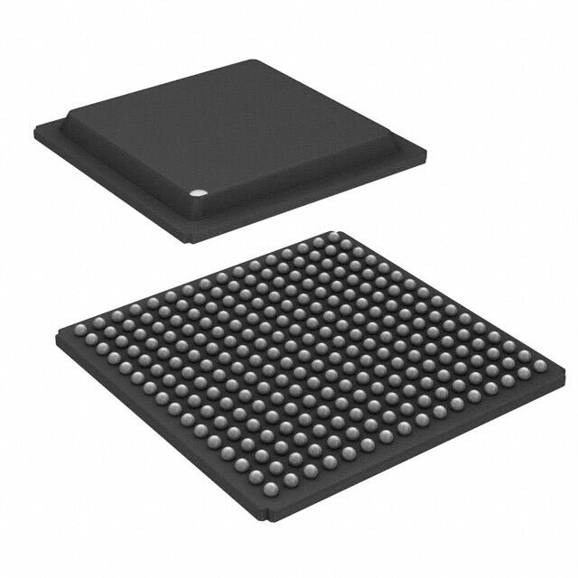
The MPC875/MPC870 comes in a 256-pin ball grid array (PBGA) package
MPC875/MPC870 PowerQUICC™ Hardware Specifications, Rev. 4
6
Freescale Semiconductor
�Features
The MPC875 block diagram is shown in Figure 1.
8-Kbyte
Instruction
Instruction Cache
Bus
System Interface Unit (SIU)
Instruction MMU
32-Entry ITLB
Embedded
MPC8xx
Processor
Core
Memory Controller
Unified
Bus
External
Internal
Bus Interface Bus Interface
Unit
Unit
8-Kbyte
Data Cache
System Functions
Data MMU
Load/Store
Bus
32-Entry DTLB
PCMCIA-ATA Interface
Slave/Master IF
Security Engine
Fast Ethernet
Controller
Controller
AESU
DEU
MDEU
Channel
DMAs
DMAs
DMAs
FIFOs
Parallel I/O
10/100
BaseT
Media Access
Control
4 Baud Rate
Generators
MIII/RMII
Parallel Interface
Port
4
Timers
Timers
Interrupt
8-Kbyte
Controllers Dual-Port RAM
32-Bit RISC Controller
and Program
ROM
SCC4
Virtual IDMA
and
Serial DMAs
SMC1
USB
SPI
I2C
Time-Slot Assigner
Serial Interface
Figure 1. MPC875 Block Diagram
MPC875/MPC870 PowerQUICC™ Hardware Specifications, Rev. 4
Freescale Semiconductor
7
�Features
The MPC870 block diagram is shown in Figure 2.
8-Kbyte
Instruction
Instruction Cache
Bus
System Interface Unit (SIU)
Instruction MMU
32-Entry ITLB
Embedded
MPC8xx
Processor
Core
Memory Controller
Unified
Bus
External
Internal
Bus Interface Bus Interface
Unit
Unit
8-Kbyte
Data Cache
System Functions
Data MMU
Load/Store
32-Entry DTLB
Bus
PCMCIA-ATA Interface
Slave/Master IF
Fast Ethernet
Controller
DMAs
DMAs
DMAs
FIFOs
Parallel I/O
10/100
BaseT
Media Access
Control
4 Baud Rate
Generators
MIII/RMII
Parallel Interface
Port
USB
4
Timers
Timers
Interrupt
8-Kbyte
Controllers Dual-Port RAM
32-Bit RISC Controller
and Program
ROM
SMC1
Virtual IDMA
and
Serial DMAs
SPI
I2C
Serial Interface
Figure 2. MPC870 Block Diagram
MPC875/MPC870 PowerQUICC™ Hardware Specifications, Rev. 4
8
Freescale Semiconductor
�Maximum Tolerated Ratings
3
Maximum Tolerated Ratings
This section provides the maximum tolerated voltage and temperature ranges for the MPC875/MPC870.
Table 2 displays the maximum tolerated ratings and Table 3 displays the operating temperatures.
Table 2. Maximum Tolerated Ratings
Rating
Symbol
Value
Unit
VDDL (core voltage)
–0.3 to 3.4
V
VDDH (I/O voltage)
–0.3 to 4
V
VDDSYN
–0.3 to 3.4
V
Difference between
VDDL and VDDSYN
100 kHz) timings.
Table 29. I2C Timing (SCL > 100 kHZ)
All Frequencies
Num
1
Characteristic
Expression
Unit
Min
Max
200
SCL clock frequency (slave)
fSCL
0
BRGCLK/48
Hz
200
SCL clock frequency (master)1
fSCL
BRGCLK/16512
BRGCLK/48
Hz
202
Bus free time between transmissions
—
1/(2.2 × fSCL)
—
s
203
Low period of SCL
—
1/(2.2 × fSCL)
—
s
204
High period of SCL
—
1/(2.2 × fSCL)
—
s
205
Start condition setup time
—
1/(2.2 × fSCL)
—
s
206
Start condition hold time
—
1/(2.2 × fSCL)
—
s
207
Data hold time
—
0
—
s
208
Data setup time
—
1/(40 × fSCL)
—
s
209
SDL/SCL rise time
—
—
1/(10 × fSCL)
s
210
SDL/SCL fall time
—
—
1/(33 × fSCL)
s
211
Stop condition setup time
—
1/2(2.2 × fSCL)
—
s
SCL frequency is given by SCL = BRGCLK_frequency/((BRG register + 3) × pre_scalar × 2).
The ratio SYNCCLK/(BRGCLK/pre_scalar) must be greater than or equal to 4/1.
Figure 64 shows the I2C bus timing.
SDA
202
203
205
204
208
207
SCL
206
209
210
211
Figure 64. I2C Bus Timing Diagram
MPC875/MPC870 PowerQUICC™ Hardware Specifications, Rev. 4
66
Freescale Semiconductor
�USB Electrical Characteristics
14 USB Electrical Characteristics
This section provides the AC timings for the USB interface.
14.1
USB Interface AC Timing Specifications
The USB Port uses the transmit clock on SCC1. Table 30 lists the USB interface timings.
Table 30. USB Interface AC Timing Specifications
All Frequencies
Name
Characteristic
Unit
Min
US1
US4
1
USBCLK frequency of operation1
Low speed
Full speed
Max
MHz
6
48
USBCLK duty cycle (measured at 1.5 V)
45
55
%
USBCLK accuracy should be ±500 ppm or better. USBCLK may be stopped to conserve power.
15 FEC Electrical Characteristics
This section provides the AC electrical specifications for the Fast Ethernet controller (FEC). Note that the
timing specifications for the MII signals are independent of system clock frequency (part speed
designation). Also, MII signals use TTL signal levels compatible with devices operating at either 5.0 or
3.3 V.
15.1
MII and Reduced MII Receive Signal Timing
The receiver functions correctly up to a MII_RX_CLK maximum frequency of 25 MHz + 1%. The
reduced MII (RMII) receiver functions correctly up to a RMII_REFCLK maximum frequency of 50 MHz
+ 1%. There is no minimum frequency requirement. In addition, the processor clock frequency must
exceed the MII_RX_CLK frequency – 1%.
Table 31 provides information on the MII receive signal timing.
Table 31. MII Receive Signal Timing
Num
Characteristic
Min
Max
Unit
M1
MII_RXD[3:0], MII_RX_DV, MII_RX_ER to MII_RX_CLK setup
5
—
ns
M2
MII_RX_CLK to MII_RXD[3:0], MII_RX_DV, MII_RX_ER hold
5
—
ns
M3
MII_RX_CLK pulse width high
35%
65%
MII_RX_CLK period
M4
MII_RX_CLK pulse width low
35%
65%
MII_RX_CLK period
M1_RMII
RMII_RXD[1:0], RMII_CRS_DV, RMII_RX_ERR to RMII_REFCLK
setup
4
—
ns
M2_RMII
RMII_REFCLK to RMII_RXD[1:0], RMII_CRS_DV, RMII_RX_ERR
hold
2
—
ns
MPC875/MPC870 PowerQUICC™ Hardware Specifications, Rev. 4
Freescale Semiconductor
67
�FEC Electrical Characteristics
Figure 65 shows MII receive signal timing.
M3
MII_RX_CLK (Input)
M4
MII_RXD[3:0] (Inputs)
MII_RX_DV
MII_RX_ER
M1
M2
Figure 65. MII Receive Signal Timing Diagram
15.2
MII and Reduced MII Transmit Signal Timing
The transmitter functions correctly up to a MII_TX_CLK maximum frequency of 25 MHz + 1%. There is
no minimum frequency requirement. In addition, the processor clock frequency must exceed the
MII_TX_CLK frequency – 1%.
Table 32 provides information on the MII transmit signal timing.
Table 32. MII Transmit Signal Timing
Num
Characteristic
Min
Max
Unit
M5
MII_TX_CLK to MII_TXD[3:0], MII_TX_EN, MII_TX_ER invalid
5
—
ns
M6
MII_TX_CLK to MII_TXD[3:0], MII_TX_EN, MII_TX_ER valid
—
25
ns
M7
MII_TX_CLK pulse width high
35%
65%
MII_TX_CLK period
M8
MII_TX_CLK pulse width low
35%
65%
MII_TX_CLK period
M20_RMII RMII_TXD[1:0], RMII_TX_EN to RMII_REFCLK setup
4
—
ns
M21_RMII RMII_TXD[1:0], RMII_TX_EN data hold from RMII_REFCLK rising
edge
2
—
ns
MPC875/MPC870 PowerQUICC™ Hardware Specifications, Rev. 4
68
Freescale Semiconductor
�FEC Electrical Characteristics
Figure 66 shows the MII transmit signal timing diagram.
M7
MII_TX_CLK (Input)
M5
M8
MII_TXD[3:0] (Outputs)
MII_TX_EN
MII_TX_ER
M6
Figure 66. MII Transmit Signal Timing Diagram
15.3
MII Async Inputs Signal Timing (MII_CRS, MII_COL)
Table 33 provides information on the MII async inputs signal timing.
Table 33. MII Async Inputs Signal Timing
Num
M9
Characteristic
Min
Max
Unit
MII_CRS, MII_COL minimum pulse width
1.5
—
MII_TX_CLK period
Figure 67 shows the MII asynchronous inputs signal timing diagram.
MII_CRS, MII_COL
M9
Figure 67. MII Async Inputs Timing Diagram
15.4
MII Serial Management Channel Timing (MII_MDIO, MII_MDC)
Table 34 provides information on the MII serial management channel signal timing. The FEC functions
correctly with a maximum MDC frequency in excess of 2.5 MHz.
Table 34. MII Serial Management Channel Timing
Num
Characteristic
Min
Max
Unit
M10
MII_MDC falling edge to MII_MDIO output invalid (minimum propagation
delay)
0
—
ns
M11
MII_MDC falling edge to MII_MDIO output valid (max prop delay)
—
25
ns
M12
MII_MDIO (input) to MII_MDC rising edge setup
10
—
ns
M13
MII_MDIO (input) to MII_MDC rising edge hold
0
—
ns
M14
MII_MDC pulse width high
40%
60%
MII_MDC period
M15
MII_MDC pulse width low
40%
60%
MII_MDC period
MPC875/MPC870 PowerQUICC™ Hardware Specifications, Rev. 4
Freescale Semiconductor
69
�FEC Electrical Characteristics
Figure 68 shows the MII serial management channel timing diagram.
M14
MM15
MII_MDC (Output)
M10
MII_MDIO (Output)
M11
MII_MDIO (Input)
M12
M13
Figure 68. MII Serial Management Channel Timing Diagram
MPC875/MPC870 PowerQUICC™ Hardware Specifications, Rev. 4
70
Freescale Semiconductor
�Mechanical Data and Ordering Information
16 Mechanical Data and Ordering Information
Table 35 identifies the packages and operating frequencies available for the MPC875/MPC870.
Table 35. Available MPC875/MPC870 Packages/Frequencies
Package Type
Plastic ball grid array
ZT suffix—Leaded
VR suffix—Lead-Free are available as needed
Plastic ball grid array
CZT suffix—Leaded
CVR suffix—Lead-Free are available as needed
Temperature (TJ)
Frequency (MHz)
Order Number
0°C to 95°C
66
KMPC875ZT66
KMPC870ZT66
MPC875ZT66
MPC870ZT66
80
KMPC875ZT80
KMPC870ZT80
MPC875ZT80
MPC870ZT80
133
KMPC875ZT133
KMPC870ZT133
MPC875ZT133
MPC870ZT133
66
KMPC875CZT66
KMPC870CZT66
MPC875CZT66
MPC870CZT66
133
KMPC875CZT133
KMPC870CZT133
MPC875CZT133
MPC870CZT133
-40°C to 100°C
MPC875/MPC870 PowerQUICC™ Hardware Specifications, Rev. 4
Freescale Semiconductor
71
�Mechanical Data and Ordering Information
16.1 Pin Assignments
Figure 69 shows the JEDEC pinout of the PBGA package as viewed from the top surface. For additional
information, see the MPC885 PowerQUICC Family User’s Manual.
NOTE
The pin numbering starts with B2 in order to conform to the JEDEC standard for
23-mm body size using a 16 × 16 array.
NOTE: This is the top view of the device.
2
3
4
5
6
7
8
9
10
11
12
13
14
15
16
17
EXTCLK MODCK1
OP0
ALEA
IPB0
BURST
IRQ6
BR
TEA
BI
CS0
CS3
RSTCONF SRESET BADDR29
OP1
AS
ALEB
IRQ2
BB
TS
TA
BDIP
CS2
CE1A
EXTAL BADDR30
IPB1
BG
GPLA4
GPLA5
WR
CE2A
CS7
WE2
WE1
VSSSYN VDDSYN HRESET BADDR28
IRQ4
IRQ3
CS1
GPLB4
CS4
GPLAB2
WE0
BSA1
BSA2
CS6
OE
BSA0
BSA3
TSIZ0
A31
WE3
TSIZ1
A26
A22
A18
VDDL
A28
A30
A25
A24
A23
A21
A20
A29
A14
A19
A27
A17
A10
A12
A15
A16
MII_MDIO A2
A8
A11
A13
PB26
PB27
A1
A6
A7
A9
B
MODCK2 TEXP
CS5
N/C
C
IPA7
GPLAB3 GPLA0
D
IPA4
IPA2
D31
IPA5
IPA3
D29
D30
IPA6
D7
D28
CLKOUT
D26
IPA0
D22
D6
D24
D25
VDDL
D18
D19
D20
D21
D5
D15
D16
D3
D2
D27
WAITA PORESET XTAL
E
F
IPA1 VSSSYN1
VDDL
VDDL
G
VDDH
VDDH
H
VDDH
GND
VDDH
J
GND
K
D14
GND
VDDL
VDDL
L
GND
VDDH
D0
VDDH
VDDH
M
D11
D9
D12
PE18
IRQ0
VDDH
IRQ7
PA2
VDDL
VDDH
N
D10
D13
D1
VDDL
P
D23
D17
IRQ1
PA0
PA4
PE14
PE31
PC6
PA6
PC11
TDO
PA15
A3
A5
A4
PE25
PA3
PE19
PE28
PE30
PA11
MII_COL
PA7
PA10
TCK
PB28
PC15
A0
PB29
PB31
PE22
R
D4
D8
T
PE26
PD8
PA1
PE27
PE15
PE17
PE21
PC7
PB19
PB24
TDI
TMS
PC12
N/C
PB30
N/C
PE20
PE23 MII-TX-EN PE16
PE29
PE24
PC13
MII-CRS
PC10
PB23
PB25
TRST
GND
PA14
N/C
U
Figure 69. Pinout of the PBGA Package—JEDEC Standard
MPC875/MPC870 PowerQUICC™ Hardware Specifications, Rev. 4
72
Freescale Semiconductor
�Mechanical Data and Ordering Information
Table 36 contains a list of the MPC875/MPC870 input and output signals and shows multiplexing and pin
assignments.
Table 36. Pin Assignments—JEDEC Standard
Name
Pin Number
Type
A[0:31]
Bidirectional
R16, N14, M14, P15, P17, P16, N15, N16, M15, N17, L14, M16,
L15, M17, K14, L16, L17, K17, G17, K15, J16, J15, G16, J14, H17, Three-state (3.3 V only)
H16, G15, K16, H14, J17, H15, F17
TSIZ0, REG
F16
Bidirectional
Three-state (3.3 V only)
TSIZ1
G14
Bidirectional
Three-state (3.3 V only)
RD/WR
D13
Bidirectional
Three-state (3.3 V only)
BURST
B9
Bidirectional
Three-state (3.3 V only)
BDIP, GPL_B5
C13
Output
TS
C11
Bidirectional
Active pull-up (3.3 V only)
TA
C12
Bidirectional
Active pull-up (3.3 V only)
TEA
B12
Open-drain
BI
B13
Bidirectional
Active pull-up (3.3 V only)
IRQ2, RSV
C9
Bidirectional
Three-state (3.3 V only)
IRQ4, KR, RETRY,
SPKROUT
E9
Bidirectional
Three-state (3.3 V only)
D[0:31]
L5, N3, L3, L2, R2, K2, H3, G2, R3, M3, N2, M2, M4, N4, K5, K3, K4, Bidirectional
P3, J2, J3, J4, J5, H2, P2, H4, H5, G5, L4, G3, F2, F3, E2
Three-state (3.3 V only)
CR, IRQ3
E10
Input
FRZ, IRQ6
B10
Bidirectional
Three-state (3.3 V only)
BR
B11
Bidirectional (3.3 V only)
BG
D10
Bidirectional (3.3 V only)
BB
C10
Bidirectional
Active pull-up (3.3 V only)
IRQ0
M6
Input (3.3 V only)
IRQ1
P5
Input (3.3 V only)
IRQ7
N5
Input (3.3 V only)
CS[0:5]
B14, E11, C14, B15, E13, B16
Output
MPC875/MPC870 PowerQUICC™ Hardware Specifications, Rev. 4
Freescale Semiconductor
73
�Mechanical Data and Ordering Information
Table 36. Pin Assignments—JEDEC Standard (continued)
Name
Pin Number
Type
CS6, CE1_B
F12
Output
CS7, CE2_B
D15
Output
WE0, BS_B0, IORD
E15
Output
WE1, BS_B1, IOWR
D17
Output
WE2, BS_B2, PCOE
D16
Output
WE3, BS_B3, PCWE
G13
Output
BS_A[0:3]
F14, E16, E17, F15
Output
GPL_A0, GPL_B0
C17
Output
OE, GPL_A1, GPL_B1
F13
Output
GPL_A[2:3], GPL_B[2:3],
CS[2–3]
E14, C16
Output
UPWAITA, GPL_A4
D11
Bidirectional (3.3 V only)
UPWAITB, GPL_B4
E12
Bidirectional
GPL_A5
D12
Output
PORESET
D5
Input (3.3 V only)
RSTCONF
C3
Input (3.3 V only)
HRESET
E7
Open-drain
SRESET
C4
Open-drain
XTAL
D6
Analog output
EXTAL
D7
Analog input (3.3 V only)
CLKOUT
G4
Output
EXTCLK
B4
Input (3.3 V only)
TEXP
B3
Output
ALE_A
B7
Output
CE1_A
C15
Output
CE2_A
D14
Output
WAIT_A
D4
Input (3.3 V only)
IP_A0
G6
Input (3.3 V only)
IP_A1
F5
Input (3.3 V only)
IP_A2, IOIS16_A
D3
Input (3.3 V only)
IP_A3
E4
Input (3.3 V only)
IP_A4
D2
Input (3.3 V only)
IP_A5
E3
Input (3.3 V only)
MPC875/MPC870 PowerQUICC™ Hardware Specifications, Rev. 4
74
Freescale Semiconductor
�Mechanical Data and Ordering Information
Table 36. Pin Assignments—JEDEC Standard (continued)
Name
Pin Number
Type
IP_A6
F4
Input (3.3 V only)
IP_A7
C2
Input (3.3 V only)
ALE_B, DSCK
C8
Bidirectional
Three-state (3.3 V only)
IP_B[0:1], IWP[0:1],
VFLS[0:1]
B8, D9
Bidirectional (3.3 V only)
OP0
B6
Bidirectional (3.3 V only)
OP1
C6
Output
OP2, MODCK1, STS
B5
Bidirectional (3.3 V only)
OP3, MODCK2, DSDO
B2
Bidirectional (3.3 V only)
BADDR[28:29]
E8, C5
Output
BADDR30, REG
D8
Output
AS
C7
Input (3.3 V only)
PA15, USBRXD
P14
Bidirectional
PA14, USBOE
U16
Bidirectional
(Optional: open-drain)
PA11, RXD4, MII1-TXD0,
RMII1-TXD0
R9
Bidirectional
(Optional: open-drain)
(5-V tolerant)
PA10, MII1-TXERR, TIN4,
CLK7
R12
Bidirectional
(Optional: open-drain)
(5-V tolerant)
PA7, CLK1, BRGO1, TIN1
R11
Bidirectional
PA6, CLK2, TOUT1
P11
Bidirectional
PA4, CTS4, MII1-TXD1,
RMII-TXD1
P7
Bidirectional
PA3, MII1-RXER,
RMII1-RXER, BRGO3
R5
Bidirectional
(5-V tolerant)
PA2, MII1-RXDV,
RMII1-CRS_DV, TXD4
N6
Bidirectional
(5-V tolerant)
PA1, MII1-RXD0,
RMII1-RXD0, BRGO4
T4
Bidirectional
(5-V tolerant)
PA0, MII1-RXD1,
RMII1-RXD1, TOUT4
P6
Bidirectional
(5-V tolerant)
PB31, SPISEL, MII1-TXCLK, T5
RMII1-REFCLK
Bidirectional
(Optional: open-drain)
(5-V tolerant)
MPC875/MPC870 PowerQUICC™ Hardware Specifications, Rev. 4
Freescale Semiconductor
75
�Mechanical Data and Ordering Information
Table 36. Pin Assignments—JEDEC Standard (continued)
Name
Pin Number
Type
PB30, SPICLK
T17
Bidirectional
(Optional: open-drain)
(5-V tolerant)
PB29, SPIMOSI
R17
Bidirectional
(Optional: open-drain)
(5-V tolerant)
PB28, SPIMISO, BRGO4
R14
Bidirectional
(Optional: open-drain)
(5-V tolerant)
PB27, I2CSDA, BRGO1
N13
Bidirectional
(Optional: open-drain)
PB26, I2CSCL, BRGO2
N12
Bidirectional
(Optional: open-drain)
PB25, SMTXD1
U13
Bidirectional
(Optional: open-drain)
(5-V tolerant)
PB24, SMRXD1
T12
Bidirectional
(Optional: open-drain)
(5-V tolerant)
PB23, SDACK1, SMSYN1
U12
Bidirectional
(Optional: open-drain)
PB19, MII1-RXD3, RTS4
T11
Bidirectional
(Optional: open-drain)
PC15, DREQ0, L1ST1
R15
Bidirectional
(5-V tolerant)
PC13, MII1-TXD3, SDACK1
U9
Bidirectional
(5-V tolerant)
PC12, MII1-TXD2, TOUT1
T15
Bidirectional
(5-V tolerant)
PC11, USBRXP
P12
Bidirectional
PC10, USBRXN, TGATE1
U11
Bidirectional
PC7, CTS4, L1TSYNCB,
USBTXP
T10
Bidirectional
(5-V tolerant)
PC6, CD4, L1RSYNCB,
USBTXN
P10
Bidirectional
(5-V tolerant)
PD8, RXD4, MII-MDC,
RMII-MDC
T3
Bidirectional
(5-V tolerant)
PE31, CLK8, L1TCLKB,
MII1-RXCLK
P9
Bidirectional
(Optional: open-drain)
PE30, L1RXDB, MII1-RXD2
R8
Bidirectional
(Optional: open-drain)
MPC875/MPC870 PowerQUICC™ Hardware Specifications, Rev. 4
76
Freescale Semiconductor
�Mechanical Data and Ordering Information
Table 36. Pin Assignments—JEDEC Standard (continued)
Name
Pin Number
Type
PE29, MII2-CRS
U7
Bidirectional
(Optional: open-drain)
PE28, TOUT3, MII2-COL
R7
Bidirectional
(Optional: open-drain)
PE27, L1RQB, MII2-RXERR, T6
RMII2-RXERR
Bidirectional
(Optional: open-drain)
PE26, L1CLKOB,
MII2-RXDV, RMII2-CRS_DV
T2
Bidirectional
(Optional: open-drain)
PE25, RXD4, MII2-RXD3,
L1ST2
R4
Bidirectional
(Optional: open-drain)
PE24, SMRXD1, BRGO1,
MII2-RXD2
U8
Bidirectional
(Optional: open-drain)
PE23, TXD4, MII2-RXCLK,
L1ST1
U4
Bidirectional
(Optional: open-drain)
PE22, TOUT2, MII2-RXD1,
RMII2-RXD1, SDACK1
P4
Bidirectional
(Optional: open-drain)
PE21, TOUT1, MII2-RXD0,
RMII2-RXD0
T9
Bidirectional
(Optional: open-drain)
PE20, MII2-TXER
U3
Bidirectional
(Optional: open-drain)
PE19, L1TXDB, MII2-TXEN,
RMII2-TXEN
R6
Bidirectional
(Optional: open-drain)
PE18, SMTXD1, MII2-TXD3
M5
Bidirectional
(Optional: open-drain)
PE17, TIN3, CLK5, BRGO3,
SMSYN1, MII2-TXD2
T8
Bidirectional
(Optional: open-drain)
PE16, L1RCLKB, CLK6,
U6
MII2-TXCLK, RMII2-REFCLK
Bidirectional
(Optional: open-drain)
PE15, TGATE1, MII2-TXD1,
RMII2-TXD1
T7
Bidirectional
PE14, MII2-TXD0,
RMII2-TXD0
P8
Bidirectional
TMS
T14
Input
(5-V tolerant)
TDI, DSDI
T13
Input
(5-V tolerant)
TCK, DSCK
R13
Input
(5-V tolerant)
TRST
U14
Input
(5-V tolerant)
MPC875/MPC870 PowerQUICC™ Hardware Specifications, Rev. 4
Freescale Semiconductor
77
�Mechanical Data and Ordering Information
Table 36. Pin Assignments—JEDEC Standard (continued)
Name
Pin Number
Type
TDO, DSDO
P13
Output
(5-V tolerant)
MII1_CRS
U10
Input
MII_MDIO
M13
Bidirectional
(5-V tolerant)
MII1_TX_EN, RMII1_TX_EN U5
Output
(5-V tolerant)
MII1_COL
R10
Input
VSSSYN
E5
PLL analog GND
VSSSYN1
F6
PLL analog GND
VDDSYN
E6
PLL analog VDD
GND
H8, H9, H10, H11, J8, J9, J10, J11, K8, K9, K10, K11, L8, L9, L10, Power
L11, U15
VDDL
F7, F8, F9, F10, F11, H6, H13, J6, J13, K6, K13, L6, L13, N7, N8,
N9, N10, N11
VDDH
G7, G8, G9, G10, G11, G12, H7, H12, J7, J12, K7, K12, L7, L12, M7, Power
M8, M9, M10, M11, M12
N/C
B17, T16, U2, U17
Power
No connect
MPC875/MPC870 PowerQUICC™ Hardware Specifications, Rev. 4
78
Freescale Semiconductor
�Mechanical Data and Ordering Information
16.2
Mechanical Dimensions of the PBGA Package
Figure 70 shows the mechanical dimensions of the PBGA package.
.
NOTES:
1. ALL DIMENSIONS ARE IN MILLIMETERS.
2. INTERPRET DIMENSIONS AND TOLERANCES PER ASME Y14.5M—1994.
3. MAXIMUM SOLDER BALL DIAMETER MEASURED PARALLEL TO DATUM A.
4. DATUM A, THE SEATING PLANE, IS DEFINED BY THE SPHERICAL CROWNS OF THE SOLDER BALLS.
Note: Solder sphere composition is 95.5%Sn 45%Ag 0.5%Cu for MPC875/MPC870VRXXX.
Solder sphere composition is 62%Sn 36%Pb 2%Ag for MPC875/MPC870ZTXXX.
Figure 70. Mechanical Dimensions and Bottom Surface Nomenclature of the PBGA Package
MPC875/MPC870 PowerQUICC™ Hardware Specifications, Rev. 4
Freescale Semiconductor
79
�Document Revision History
17 Document Revision History
Table 37 lists significant changes between revisions of this hardware specification.
Table 37. Document Revision History
Revision
Number
Date
0
2/2003
Initial release.
0.1
3/2003
Took out the time-slot assigner and changed the SCC for SCC3 to SCC4.
0.2
5/2003
Changed the package drawing, removed all references to Data Parity. Changed the SPI Master Timing
Specs. 162 and 164. Added the RMII and USB timing. Added the 80-MHz timing.
0.3
5/2003
Made sure the pin types were correct. Changed the Features list to agree with the MPC885.
0.4
5/2003
Corrected the signals that had overlines on them. Made corrections on two pins that were typos.
0.5
5/2003
Changed the pin descriptions for PD8 and PD9.
0.6
5/2003
Changed a few typos. Put back the I2C. Put in the new reset configuration, corrected the USB timing.
0.7
6/2003
Changed the pin descriptions per the June 22 spec, removed Utopia from the pin descriptions,
changed PADIR, PBDIR, PCDIR and PDDIR to be 0 in the Mandatory Reset Config.
0.8
8/2003
Added the reference to USB 2.0 to the Features list and removed 1.1 from USB on the block diagrams.
0.9
8/2003
Changed the USB description to full-/low-speed compatible.
1.0
9/2003
Added the DSP information in the Features list.
Put a new sentence under Mechanical Dimensions.
Fixed table formatting.
Nontechnical edits.
Released to the external web.
1.1
10/2003
Added TDMb to the MPC875 Features list, the MPC875 Block Diagram, added 13.5 Serial Interface
AC Electrical Specifications, and removed TDMa from the pin descriptions.
2.0
12/2003
Changed DBGC in the Mandatory Reset Configuration to X1.
Changed the maximum operating frequency to 133 MHz.
Put the timing in the 80 MHz column.
Put in the orderable part numbers.
Rounded the timings to hundredths in the 80 MHz column.
Put the pin numbers in footnotes by the maximum currents in Table 6.
Changed 22 and 41 in the Timing.
Put TBD in the Thermal table.
Changes
MPC875/MPC870 PowerQUICC™ Hardware Specifications, Rev. 4
80
Freescale Semiconductor
�Document Revision History
Table 37. Document Revision History (continued)
Revision
Number
Date
3.0
1/07/2004
7/19/2004
4
08/2007
Changes
•
•
•
•
•
Added sentence to Spec B1A about EXTCLK and CLKOUT being in alignment for integer values.
Added a footnote to Spec 41 specifying that EDM = 1.
Added the thermal numbers to Table 4.
Added RMII1_EN under M1II_EN in Table 36, Pin Assignments.
Added a table footnote to Table 6, DC Electrical Specifications, about meeting the VIL Max of the
I2C Standard.
• Put the new part numbers in the Ordering Information Section.
• Updated template.
• On page 1, updated first paragraph and added a second paragraph.
• After Table 2, inserted a new figure showing the undershoot/overshoot voltage (Figure 3) and
renumbered the rest of the figures.
• In Table 10, for reset timings B29f and B29g added footnote indicating that the formula only applies
to bus operation up to 50 MHz.
• In Figure 5, changed all reference voltage measurement points from 0.2 and 0.8 V to 50% level.
• In Table 18, changed num 46 description to read, “TA assertion to rising edge ...”
• In Figure 43, changed TA to reflect the rising edge of the clock.
MPC875/MPC870 PowerQUICC™ Hardware Specifications, Rev. 4
Freescale Semiconductor
81
�Document Revision History
THIS PAGE INTENTIONALLY LEFT BLANK
MPC875/MPC870 PowerQUICC™ Hardware Specifications, Rev. 4
82
Freescale Semiconductor
�Document Revision History
THIS PAGE INTENTIONALLY LEFT BLANK
MPC875/MPC870 PowerQUICC™ Hardware Specifications, Rev. 4
Freescale Semiconductor
83
�How to Reach Us:
Home Page:
www.freescale.com
Web Support:
http://www.freescale.com/support
USA/Europe or Locations Not Listed:
Freescale Semiconductor, Inc.
Technical Information Center, EL516
2100 East Elliot Road
Tempe, Arizona 85284
+1-800-521-6274 or
+1-480-768-2130
www.freescale.com/support
Europe, Middle East, and Africa:
Freescale Halbleiter Deutschland GmbH
Technical Information Center
Schatzbogen 7
81829 Muenchen, Germany
+44 1296 380 456 (English)
+46 8 52200080 (English)
+49 89 92103 559 (German)
+33 1 69 35 48 48 (French)
www.freescale.com/support
Information in this document is provided solely to enable system and software
implementers to use Freescale Semiconductor products. There are no express or
implied copyright licenses granted hereunder to design or fabricate any integrated
circuits or integrated circuits based on the information in this document.
Freescale Semiconductor reserves the right to make changes without further notice to
any products herein. Freescale Semiconductor makes no warranty, representation or
guarantee regarding the suitability of its products for any particular purpose, nor does
Freescale Semiconductor assume any liability arising out of the application or use of
any product or circuit, and specifically disclaims any and all liability, including without
limitation consequential or incidental damages. “Typical” parameters which may be
provided in Freescale Semiconductor data sheets and/or specifications can and do
vary in different applications and actual performance may vary over time. All operating
parameters, including “Typicals” must be validated for each customer application by
customer’s technical experts. Freescale Semiconductor does not convey any license
Japan:
Freescale Semiconductor Japan Ltd.
Headquarters
ARCO Tower 15F
1-8-1, Shimo-Meguro, Meguro-ku
Tokyo 153-0064
Japan
0120 191014 or
+81 3 5437 9125
support.japan@freescale.com
under its patent rights nor the rights of others. Freescale Semiconductor products are
Asia/Pacific:
Freescale Semiconductor Hong Kong Ltd.
Technical Information Center
2 Dai King Street
Tai Po Industrial Estate
Tai Po, N.T., Hong Kong
+800 2666 8080
support.asia@freescale.com
claims, costs, damages, and expenses, and reasonable attorney fees arising out of,
For Literature Requests Only:
Freescale Semiconductor
Literature Distribution Center
P.O. Box 5405
Denver, Colorado 80217
+1-800 441-2447 or
+1-303-675-2140
Fax: +1-303-675-2150
LDCForFreescaleSemiconductor
@hibbertgroup.com
Document Number: MPC875EC
Rev. 4
08/2007
not designed, intended, or authorized for use as components in systems intended for
surgical implant into the body, or other applications intended to support or sustain life,
or for any other application in which the failure of the Freescale Semiconductor product
could create a situation where personal injury or death may occur. Should Buyer
purchase or use Freescale Semiconductor products for any such unintended or
unauthorized application, Buyer shall indemnify and hold Freescale Semiconductor
and its officers, employees, subsidiaries, affiliates, and distributors harmless against all
directly or indirectly, any claim of personal injury or death associated with such
unintended or unauthorized use, even if such claim alleges that Freescale
Semiconductor was negligent regarding the design or manufacture of the part.
Freescale™ and the Freescale logo are trademarks of Freescale Semiconductor, Inc.
The Power Architecture and Power.org word marks and the Power and Power.org logos
and related marks are trademarks and service marks licensed by Power.org. IEEE
802.3, 802.11i, and 1149.1 are trademarks or registered trademarks of the Institute of
Electrical and Electronics Engineers, Inc. (IEEE). This product is not endorsed or
approved by the IEEE. All other product or service names are the property of their
respective owners.
© Freescale Semiconductor, Inc., 2003–2007. All rights reserved.
�


 工商网监
湘ICP备2023018690号
工商网监
湘ICP备2023018690号
