MC33932
5.0 A throttle control H-bridge
Rev. 6.0 — 10 September 2018
1
Data sheet: technical data
General description
The 33932 is a monolithic H-bridge power IC in a robust thermally enhanced package.
The 33932 has two independent monolithic H-bridge power ICs in the same package.
They are designed primarily for automotive electronic throttle control, but are applicable
to any low voltage DC servo motor control application within the current and voltage limits
stated in this specification. It meets the stringent requirements of automotive applications
and is fully AEC-Q100 grade 1 qualified.
Each H-bridge in the 33932 is able to control inductive loads with currents up to 5.0 A
peak. RMS current capability is subject to the degree of heat sinking provided to the
device package. Internal peak-current limiting (regulation) is activated at load currents
above 6.5 A ± 1.5 A. Output loads can be pulse-width modulated at frequencies up to
11 kHz. A load current feedback feature provides a proportional (0.24 % of the load
current) current output suitable for monitoring by a microcontroller’s A/D input. A status
flag output reports undervoltage, overcurrent and overtemperature fault conditions.
Two independent inputs provide polarity control of two half-bridge totem pole outputs.
Two independent disable inputs are provided to force the H-bridge outputs to 3-state
(high-impedance OFF state).
VPWR
VDD
33932
SFA
FBA
MCU
IN1
IN2
D1
EN/D2
IN3
IN4
D3
EN/D4
FBB
VPWRA
CCPA
OUT1
OUT2
PGNDA
AGNDA
MOTOR
VPWR
VPWRB
CCPB
OUT3
MOTOR
VDD
SFB
PGNDB
AGNDB
OUT4
Figure 1. Simplified application diagram
2
Features and benefits
•
•
•
•
•
•
•
8.0 to 28 V continuous operation (transient operation from 5.0 to 40 V)
235 mΩ maximum RDS(on) @ TJ = 150 °C (each H-bridge MOSFET)
3.0 V and 5.0 V TTL / CMOS logic compatible inputs
Output short-circuit protection (short to VPWR or GND)
Overcurrent limiting (regulation) via internal constant-off-time PWM
Temperature dependent current limit threshold reduction
All inputs have an internal source/sink to define the default (floating input) state
�MC33932
NXP Semiconductors
5.0 A throttle control H-bridge
• Sleep mode with current draw < 50 µA (each half with inputs floating or set to match
default logic states)
• AEC-Q100 grade 1 qualified
3
Applications
•
•
•
•
•
•
4
Electronic throttle control (ETC)
Exhaust gas recirculation (EGR)
Turbo flap control
Industrial and medical pumps
Stepper motor control
Dual motor drive
Ordering information
Table 1. Ordering information
Type number
[1]
Package
Name
Description
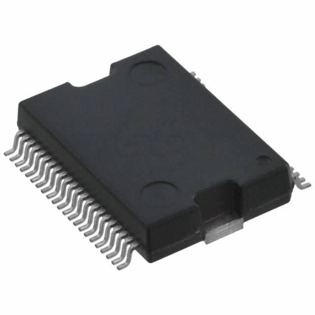
MC33932VW
HSOP44
HSOP44, plastic, thermal enhanced small
outline package; 44 terminals; 0.65 mm pitch;
15.9 mm x 11 mm x 3 mm body
MC33932EK
HSOP54
HSOP54, plastic, heat sink small outline
package; 54 terminals; 0.65 mm pitch; 17.9
mm x 7.5 mm x 2.65 mm body
[1]
Operating
temperature
Version
SOT1305-2
TA = −40 °C to 125 °C
SOT1747-4
To order parts in tape and reel, add the R2 suffix to the part number.
MC33932
Data sheet: technical data
All information provided in this document is subject to legal disclaimers.
Rev. 6.0 — 10 September 2018
© NXP B.V. 2018. All rights reserved.
2 / 32
�MC33932
NXP Semiconductors
5.0 A throttle control H-bridge
5
Block diagram
VPWRA
LOGIC SUPPLY
CCPA
VDD
VCP CHARGE
PUMP
HS1
HS2
OUT1
TO GATES
OUT2
HS1
LS1
IN1
IN2
EN/D2
D1
LS1
LS2
HS2
GATE DRIVE
AND
PROTECTION
LOGIC
PGND
LS2
VSENSE
SFA
CURRENT MIRROR
AND
CONSTANT OFF-TIME
PWM CURRENT REGULATOR
ILIM PWM
FBA
H-Bridge A
AGNDA
PGNDA
H-Bridge B
LOGIC SUPPLY
CCPB
VDD
VPWRB
VCP CHARGE
PUMP
HS1
HS2
OUT3
TO GATES
OUT4
HS1
IN3
LS1
IN4
EN/D4
D3
LS1
LS2
HS2
GATE DRIVE
AND
PROTECTION
LOGIC
SFB
PGND
LS2
VSENSE
ILIM PWM
FBB
AGNDB
CURRENT MIRROR
AND
CONSTANT OFF-TIME
PWM CURRENT REGULATOR
PGNDB
Figure 2. Block diagram
MC33932
Data sheet: technical data
All information provided in this document is subject to legal disclaimers.
Rev. 6.0 — 10 September 2018
© NXP B.V. 2018. All rights reserved.
3 / 32
�MC33932
NXP Semiconductors
5.0 A throttle control H-bridge
6
Pinning information
6.1 Pinning
Figure 3. Pin configuration for HSOP44
MC33932
Data sheet: technical data
All information provided in this document is subject to legal disclaimers.
Rev. 6.0 — 10 September 2018
© NXP B.V. 2018. All rights reserved.
4 / 32
�MC33932
NXP Semiconductors
5.0 A throttle control H-bridge
Figure 4. Pin configuration for HSOP54
6.2 Pin description
For functional description of each pin, see Section 7.2 "Functional pin description".
Table 2. Pin description
Symbol
Pin HSOP
(VW)
Pin SOICW-EP Function
(EK)
Name
D1
1
3
Logic input
Disable input 1 When D1 is logic high, both OUT1 and
(active high)
OUT2 are 3-stated. Schmitt trigger input
with ~80 μA source so default condition =
disabled.
FBA
2
4
Analog output
Feedback
MC33932
Data sheet: technical data
All information provided in this document is subject to legal disclaimers.
Rev. 6.0 — 10 September 2018
Description
H-bridge A load current feedback output
provides ground referenced 0.24 % of
the high-side output current (tie to GND
through a resistor if not used)
© NXP B.V. 2018. All rights reserved.
5 / 32
�MC33932
NXP Semiconductors
5.0 A throttle control H-bridge
Symbol
Pin HSOP
(VW)
Pin SOICW-EP Function
(EK)
Name
Description
EN/D2
3
5
Logic input
Enable input
When EN/D2 is logic high, the H-bridge A
is operational. When EN/D2 is logic low,
the H-bridge A outputs are 3-stated and
placed in Sleep mode (logic input with ~
80 μA sink so default condition = Sleep
mode).
VPWRA
4, 5, 6, 39, 40
1, 9, 46, 53
Power input
Positive power
supply
These pins must be connected together
physically as close as possible and
directly soldered down to a wide, thick,
low resistance supply plane on the PCB.
OUT1
7, 8, 9
10, 11
Power output
H-bridge output H-bridge A source of HS1 and drain LS1
1
PGNDA
10, 11, 34, 35
12, 13, 42, 43
Power ground
Power ground
High-current power ground pins must
be connected together physically as
close as possible and directly soldered
down to a wide, thick, low resistance
ground plane on the PCB. PGNDA
should be connected to PGNDB with a
low-impedance path.
PGNDB
12, 13, 32, 33
15, 16, 39, 40
Power ground
Power ground
High-current power ground pins must
be connected together physically as
close as possible and directly soldered
down to a wide, thick, low resistance
ground plane on the PCB. PGNDB
should be connected to PGNDA with a
low-impedance path.
OUT4
14, 15, 16
17, 18
Power output
H-bridge output H-bridge B source of HS2 and drain of
4
LS2
VPWRB
17, 18, 26, 27,
28
19, 26, 28, 36
Power input
Positive power
supply
These pins must be connected together
physically as close as possible and
directly soldered down to a wide, thick,
low resistance supply plane on the PCB.
CCPB
19
20
Analog output
Charge pump
capacitor
External reservoir capacitor connection
for H-bridge B internal charge pump;
connected to VPWRB. Allowable values
[1]
are 30 nF to 100 nF
IN4
20
23
Logic input
Input 4
Logic input control of OUT4
IN3
21
24
Logic input
Input 3
Logic input control of OUT3
SFB
22
25
Logic output open drain
Status flag B
(active low)
H-bridge B open drain active low Status
flag output (requires an external pull-up
resistor to VDD. Maximum permissible
load current < 0.5 mA. Maximum VSFLOW
< 0.4 V at 0.3 mA. Maximum permissible
pull-up voltage < 7.0 V.
D3
23
30
Logic input
Disable input 3 When D3 is logic high, both OUT3 and
(active high)
OUT4 are 3-stated. Schmitt trigger input
with ~80 μA source so default condition =
disabled.
MC33932
Data sheet: technical data
All information provided in this document is subject to legal disclaimers.
Rev. 6.0 — 10 September 2018
© NXP B.V. 2018. All rights reserved.
6 / 32
�MC33932
NXP Semiconductors
5.0 A throttle control H-bridge
Symbol
Pin HSOP
(VW)
Pin SOICW-EP Function
(EK)
Name
Description
FBB
24
31
Analog output
Feedback B
H-bridge B load current feedback output
provides ground referenced 0.24 % of
the high-side output current (tie to GND
through a resistor if not used)
EN/D4
25
32
Logic input
Enable input
When EN/D4 is logic high, H-bridge
B is operational. When EN/D4 is logic
low, the H-bridge B outputs are 3-stated
and H-bridge B is placed in Sleep mode
(logic input with ~ 80 μA sink so default
condition = Sleep mode).
OUT3
29, 30, 31
37, 38
Power output
H-bridge output H-bridge B source of HS1 and drain of
3
LS1
OUT2
36, 37, 38
44, 45
Power output
H-bridge output H-bridge A source of HS2 and drain of
2
LS2
CCPA
41
47
Analog output
Charge pump
capacitor
External reservoir capacitor connection
for H-bridge B internal charge pump;
connected to VPWRB. Allowable values
[1]
are 30 nF to 100 nF.
IN2
42
50
Logic input
Input 2
Logic input control of OUT2
IN1
43
51
Logic input
Input 1
Logic input control of OUT1; e.g., when
IN1 is logic high, OUT1 is set to VPWRA,
and when IN1 is logic low, OUT1 is set to
PGNDA. Schmitt trigger input with ~ 80
μA source so default condition = OUT1
high.
SFA
44
52
Logic output open drain
Status flag
(active low)
H-bridge A open drain active low status
flag output requires an external pull-up
resistor to VDD. Maximum permissible
load current < 0.5 mA. Maximum VSFLOW
< 0.4 V at 0.3 mA. Maximum permissible
pull-up voltage < 7.0 V.
AGNDA
AGNDB
TAB
54
27
Analog ground
Analog signal
ground
The low-current analog signal ground
must be connected to PGND via lowimpedance path (


 工商网监
湘ICP备2023018690号
工商网监
湘ICP备2023018690号
