Freescale Semiconductor Inc.
Data Sheet: Technical Data
Document Number: IMX6DQCEC
Rev. 4, 07/2015
MCIMX6QxExxxxC
MCIMX6QxExxxxD
MCIMX6DxExxxxC
MCIMX6DxExxxxD
i.MX 6Dual/6Quad
Applications Processors
for Consumer Products
Package Information
Case FCPBGA 21 x 21 mm, 0.8 mm pitch
Ordering Information
See Table 1 on page 3
1
Introduction
The i.MX 6Dual and i.MX 6Quad processors represent
Freescale Semiconductor’s latest achievement in
integrated multimedia applications processors. These
processors are part of a growing family of
multimedia-focused products that offer high
performance processing and are optimized for lowest
power consumption.
The i.MX 6Dual/6Quad processors feature the Freescale
advanced implementation of the quad
ARM® Cortex®-A9 core, which operates at speeds up to
1 GHz. They include 2D and 3D graphics processors, 3D
1080p video processing, and integrated power
management. Each processor provides a 64-bit
DDR3/LVDDR3/LPDDR2-1066 memory interface and
a number of other interfaces for connecting peripherals,
such as WLAN, Bluetooth®, GPS, hard drive, displays,
and camera sensors.
The i.MX 6Dual/6Quad processors are specifically
useful for applications such as the following:
• Netbooks (web tablets)
© 2012-2015 Freescale Semiconductor, Inc. All rights reserved.
1
2
3
4
5
6
7
Introduction . . . . . . . . . . . . . . . . . . . . . . . . . . . . . . . . . . . . 1
1.1 Ordering Information . . . . . . . . . . . . . . . . . . . . . . . . 3
1.2 Features . . . . . . . . . . . . . . . . . . . . . . . . . . . . . . . . . 4
1.3 Updated Signal Naming Convention . . . . . . . . . . . . 7
Architectural Overview . . . . . . . . . . . . . . . . . . . . . . . . . . . 9
2.1 Block Diagram . . . . . . . . . . . . . . . . . . . . . . . . . . . . . 9
Modules List . . . . . . . . . . . . . . . . . . . . . . . . . . . . . . . . . . 10
3.1 Special Signal Considerations. . . . . . . . . . . . . . . . 18
3.2 Recommended Connections for Unused Analog
Interfaces. . . . . . . . . . . . . . . . . . . . . . . . . . . . . . . . 18
Electrical Characteristics. . . . . . . . . . . . . . . . . . . . . . . . . 19
4.1 Chip-Level Conditions . . . . . . . . . . . . . . . . . . . . . . 19
4.2 Power Supplies Requirements and Restrictions . . 32
4.3 Integrated LDO Voltage Regulator Parameters . . . 33
4.4 PLL Electrical Characteristics . . . . . . . . . . . . . . . . 35
4.5 On-Chip Oscillators . . . . . . . . . . . . . . . . . . . . . . . . 36
4.6 I/O DC Parameters . . . . . . . . . . . . . . . . . . . . . . . . 38
4.7 I/O AC Parameters . . . . . . . . . . . . . . . . . . . . . . . . 42
4.8 Output Buffer Impedance Parameters . . . . . . . . . . 47
4.9 System Modules Timing . . . . . . . . . . . . . . . . . . . . 51
4.10 General-Purpose Media Interface (GPMI) Timing. 66
4.11 External Peripheral Interface Parameters . . . . . . . 75
Boot Mode Configuration . . . . . . . . . . . . . . . . . . . . . . . 141
5.1 Boot Mode Configuration Pins. . . . . . . . . . . . . . . 141
5.2 Boot Devices Interfaces Allocation . . . . . . . . . . . 142
Package Information and Contact Assignments . . . . . . 144
6.1 Updated Signal Naming Convention . . . . . . . . . . 144
6.2 21 x 21 mm Package Information . . . . . . . . . . . . 145
Revision History . . . . . . . . . . . . . . . . . . . . . . . . . . . . . . 167
�Introduction
•
•
•
•
•
•
Nettops (Internet desktop devices)
High-end mobile Internet devices (MID)
High-end PDAs
High-end portable media players (PMP) with HD video capability
Gaming consoles
Portable navigation devices (PND)
The i.MX 6Dual/6Quad processors offers numerous advanced features, such as:
• Applications processors—The processors enhance the capabilities of high-tier portable
applications by fulfilling the ever increasing MIPS needs of operating systems and games.
Freescale’s Dynamic Voltage and Frequency Scaling (DVFS) provides significant power
reduction, allowing the device to run at lower voltage and frequency with sufficient MIPS for tasks
such as audio decode.
• Multilevel memory system—The multilevel memory system of each processor is based on the L1
instruction and data caches, L2 cache, and internal and external memory. The processors support
many types of external memory devices, including DDR3, low voltage DDR3, LPDDR2, NOR
Flash, PSRAM, cellular RAM, NAND Flash (MLC and SLC), OneNAND™, and managed
NAND, including eMMC up to rev 4.4/4.41.
• Smart speed technology—The processors have power management throughout the device that
enables the rich suite of multimedia features and peripherals to consume minimum power in both
active and various low power modes. Smart speed technology enables the designer to deliver a
feature-rich product, requiring levels of power far lower than industry expectations.
• Dynamic voltage and frequency scaling—The processors improve the power efficiency of devices
by scaling the voltage and frequency to optimize performance.
• Multimedia powerhouse—The multimedia performance of each processor is enhanced by a
multilevel cache system, Neon® MPE (Media Processor Engine) co-processor, a multi-standard
hardware video codec, 2 autonomous and independent image processing units (IPU), and a
programmable smart DMA (SDMA) controller.
• Powerful graphics acceleration—Each processor provides three independent, integrated graphics
processing units: an OpenGL® ES 2.0 3D graphics accelerator with four shaders (up to 200 MTri/s
and OpenCL support), 2D graphics accelerator, and dedicated OpenVG™ 1.1 accelerator.
• Interface flexibility—Each processor supports connections to a variety of interfaces: LCD
controller for up to four displays (including parallel display, HDMI1.4, MIPI display, and LVDS
display), dual CMOS sensor interface (parallel or through MIPI), high-speed USB on-the-go with
PHY, high-speed USB host with PHY, multiple expansion card ports (high-speed MMC/SDIO host
and other), 10/100/1000 Mbps Gigabit Ethernet controller, and a variety of other popular interfaces
(such as UART, I2C, and I2S serial audio, SATA-II, and PCIe-II).
• Advanced security—The processors deliver hardware-enabled security features that enable secure
e-commerce, digital rights management (DRM), information encryption, secure boot, and secure
software downloads. The security features are discussed in detail in the i.MX 6Dual/6Quad
security reference manual (IMX6DQ6SDLSRM).
i.MX 6Dual/6Quad Applications Processors for Consumer Products, Rev. 4, 07/2015
2
Freescale Semiconductor Inc.
�Introduction
•
1.1
Integrated power management—The processors integrate linear regulators and internally generate
voltage levels for different domains. This significantly simplifies system power management
structure.
Ordering Information
Table 1shows examples of orderable part numbers covered by this data sheet. This table does not include
all possible orderable part numbers. The latest part numbers are available on freescale.com/imx6series. If
your desired part number is not listed in the table, or you have questions about available parts, see
freescale.com/imx6series or contact your Freescale representative.
Table 1. Example Orderable Part Numbers
1
Part Number
Quad/Dual CPU
Options
Speed1
Grade
Temperature
Grade
Package
MCIMX6Q5EYM10AC
i.MX 6Quad
With VPU, GPU
1 GHz
Extended
Consumer
21 mm x 21 mm, 0.8 mm
pitch, FCPBGA (non-lidded)
MCIMX6Q5EYM10AD
i.MX 6Quad
With VPU, GPU
1 GHz
Extended
Consumer
21 mm x 21 mm, 0.8 mm
pitch, FCPBGA (non-lidded)
SCIMX6Q5EYM10CC
i.MX 6Quad
With VPU, GPU,
HDCP
1 GHz
Extended
Consumer
21 mm x 21 mm, 0.8 mm
pitch, FCPBGA (non-lidded)
SCIMX6Q5EYM10CD
i.MX 6Quad
With VPU, GPU,
HDCP
1 GHz
Extended
Consumer
21 mm x 21 mm, 0.8 mm
pitch, FCPBGA (non-lidded)
MCIMX6D5EYM10AC
i.MX 6Dual
With VPU, GPU
1 GHz
Extended
Consumer
21 mm x 21 mm, 0.8 mm
pitch, FCPBGA (non-lidded)
MCIMX6D5EYM10AD
i.MX 6Dual
With VPU, GPU
1 GHz
Extended
Consumer
21 mm x 21 mm, 0.8 mm
pitch, FCPBGA (non-lidded)
SCIMX6D5EYM10CC
i.MX 6Dual
With VPU, GPU,
HDCP
1 GHz
Extended
Consumer
21 mm x 21 mm, 0.8 mm
pitch, FCPBGA (non-lidded)
SCIMX6D5EYM10CD
i.MX 6Dual
With VPU, GPU,
HDCP
1 GHz
Extended
Consumer
21 mm x 21 mm, 0.8 mm
pitch, FCPBGA (non-lidded)
If a 24 MHz input clock is used (required for USB), the maximum SoC speed is limited to 996 MHz.
Figure 1 describes the part number nomenclature to identify the characteristics of the specific part number
you have (for example, cores, frequency, temperature grade, fuse options, silicon revision). Figure 1
applies to the i.MX 6Dual/6Quad.
The two characteristics that identify which data sheet a specific part applies to are the part number series
field and the temperature grade (junction) field:
• The i.MX 6Dual/6Quad Automotive and Infotainment Applications Processors data sheet
(IMX6DQAEC) covers parts listed with “A (Automotive temp)”
• The i.MX 6Dual/6Quad Applications Processors for Consumer Products data sheet (IMX6DQCEC)
covers parts listed with “D (Commercial temp)” or “E (Extended Commercial temp)”
• The i.MX 6Dual/6Quad Applications Processors for Industrial Products data sheet (IMX6DQIEC)
covers parts listed with “C (Industrial temp)”
i.MX 6Dual/6Quad Applications Processors for Consumer Products, Rev. 4, 07/2015
Freescale Semiconductor Inc.
3
�Introduction
Ensure that you have the right data sheet for your specific part by checking the temperature grade
(junction) field and matching it to the right data sheet. If you have questions, see freescale.com/imx6series
or contact your Freescale representative.
MC
Qualification level
IMX6
X
@
+
VV
$$
%
A
MC
Prototype Samples
PC
Mass Production
MC
Special
SC
Part # series
X
i.MX 6Quad
Q
i.MX 6Dual
D
Silicon revision1
A
Rev 1.2
C
Rev 1.3
D
Fusing
%
Default Setting
A
HDCP Enabled
C
Frequency
Part differentiator
@
Industrial – w/ VPU, GPU, no MLB
7
Automotive – w/ VPU, GPU
6
Consumer – w/ VPU, GPU
5
Automotive – w/ GPU, no VPU
4
Temperature Tj
+
Extended Commercial: -20 to + 105°C
E
Industrial: -40 to +105 °C
C
Automotive: -40 to + 125°C
A
$$
800 MHz (Industrial grade)
08
852 MHz (Automotive grade)
08
1 GHz3
10
1.2 GHz
12
Package type
RoHS
2
FCPBGA 21x21 0.8mm (lidded)
VT
FCPBGA 21x21 0.8mm (non lidded)
YM
1. See the freescale.com\imx6series Web page for latest information on the available silicon revision.
2. If a 24 MHz input clock is used (required for USB), the maximum SoC speed is limited to 792 MHz.
3. If a 24 MHz input clock is used (required for USB), the maximum SoC speed is limited to 996 MHz.
Figure 1. Part Number Nomenclature—i.MX 6Quad and i.MX 6Dual
1.2
Features
The i.MX 6Dual/6Quad processors are based on ARM Cortex-A9 MPCore platform, which has the
following features:
• ARM Cortex-A9 MPCore 4xCPU processor (with TrustZone®)
• The core configuration is symmetric, where each core includes:
— 32 KByte L1 Instruction Cache
— 32 KByte L1 Data Cache
— Private Timer and Watchdog
— Cortex-A9 NEON MPE (Media Processing Engine) Co-processor
The ARM Cortex-A9 MPCore complex includes:
• General Interrupt Controller (GIC) with 128 interrupt support
• Global Timer
• Snoop Control Unit (SCU)
i.MX 6Dual/6Quad Applications Processors for Consumer Products, Rev. 4, 07/2015
4
Freescale Semiconductor Inc.
�Introduction
•
•
•
•
1 MB unified I/D L2 cache, shared by two/four cores
Two Master AXI (64-bit) bus interfaces output of L2 cache
Frequency of the core (including Neon and L1 cache) as per Table 6.
NEON MPE coprocessor
— SIMD Media Processing Architecture
— NEON register file with 32x64-bit general-purpose registers
— NEON Integer execute pipeline (ALU, Shift, MAC)
— NEON dual, single-precision floating point execute pipeline (FADD, FMUL)
— NEON load/store and permute pipeline
The SoC-level memory system consists of the following additional components:
— Boot ROM, including HAB (96 KB)
— Internal multimedia / shared, fast access RAM (OCRAM, 256 KB)
— Secure/non-secure RAM (16 KB)
• External memory interfaces:
— 16-bit, 32-bit, and 64-bit DDR3-1066, LVDDR3-1066, and 1/2 LPDDR2-1066 channels,
supporting DDR interleaving mode, for 2x32 LPDDR2-1066
— 8-bit NAND-Flash, including support for Raw MLC/SLC, 2 KB, 4 KB, and 8 KB page size,
BA-NAND, PBA-NAND, LBA-NAND, OneNAND™ and others. BCH ECC up to 40 bit.
— 16/32-bit NOR Flash. All EIMv2 pins are muxed on other interfaces.
— 16/32-bit PSRAM, Cellular RAM
Each i.MX 6Dual/6Quad processor enables the following interfaces to external devices (some of them are
muxed and not available simultaneously):
• Hard Disk Drives—SATA II, 3.0 Gbps
• Displays—Total five interfaces available. Total raw pixel rate of all interfaces is up to 450
Mpixels/sec, 24 bpp. Up to four interfaces may be active in parallel.
— One Parallel 24-bit display port, up to 225 Mpixels/sec (for example, WUXGA at 60 Hz or dual
HD1080 and WXGA at 60 Hz)
— LVDS serial ports—One port up to 165 Mpixels/sec or two ports up to 85 MP/sec (for example,
WUXGA at 60 Hz) each
— HDMI 1.4 port
— MIPI/DSI, two lanes at 1 Gbps
• Camera sensors:
— Parallel Camera port (up to 20 bit and up to 240 MHz peak)
— MIPI CSI-2 serial camera port, supporting up to 1000 Mbps/lane in 1/2/3-lane mode and up to
800 Mbps/lane in 4-lane mode. The CSI-2 Receiver core can manage one clock lane and up to
four data lanes. Each i.MX 6Dual/6Quad processor has four lanes.
• Expansion cards:
— Four MMC/SD/SDIO card ports all supporting:
i.MX 6Dual/6Quad Applications Processors for Consumer Products, Rev. 4, 07/2015
Freescale Semiconductor Inc.
5
�Introduction
•
•
•
– 1-bit or 4-bit transfer mode specifications for SD and SDIO cards up to UHS-I SDR-104
mode (104 MB/s max)
– 1-bit, 4-bit, or 8-bit transfer mode specifications for MMC cards up to 52 MHz in both SDR
and DDR modes (104 MB/s max)
USB:
— One High Speed (HS) USB 2.0 OTG (Up to 480 Mbps), with integrated HS USB PHY
— Three USB 2.0 (480 Mbps) hosts:
– One HS host with integrated High Speed PHY
– Two HS hosts with integrated HS-IC USB (High Speed Inter-Chip USB) PHY
Expansion PCI Express port (PCIe) v2.0 one lane
— PCI Express (Gen 2.0) dual mode complex, supporting Root complex operations and Endpoint
operations. Uses x1 PHY configuration.
Miscellaneous IPs and interfaces:
— SSI block capable of supporting audio sample frequencies up to 192 kHz stereo inputs and
outputs with I2S mode
— ESAI is capable of supporting audio sample frequencies up to 260kHz in I2S mode with 7.1
multi channel outputs
— Five UARTs, up to 5.0 Mbps each:
– Providing RS232 interface
– Supporting 9-bit RS485 multidrop mode
– One of the five UARTs (UART1) supports 8-wire while others four supports 4-wire. This is
due to the SoC IOMUX limitation, since all UART IPs are identical.
— Five eCSPI (Enhanced CSPI)
— Three I2C, supporting 400 kbps
— Gigabit Ethernet Controller (IEEE1588 compliant), 10/100/10001 Mbps
— Four Pulse Width Modulators (PWM)
— System JTAG Controller (SJC)
— GPIO with interrupt capabilities
— 8x8 Key Pad Port (KPP)
— Sony Philips Digital Interconnect Format (SPDIF), Rx and Tx
— Two Controller Area Network (FlexCAN), 1 Mbps each
— Two Watchdog timers (WDOG)
— Audio MUX (AUDMUX)
— MLB (MediaLB) provides interface to MOST Networks (150 Mbps) with the option of DTCP
cipher accelerator
1. The theoretical maximum performance of 1 Gbps ENET is limited to 470 Mbps (total for Tx and Rx) due to internal bus
throughput limitations. The actual measured performance in optimized environment is up to 400 Mbps. For details, see the
ERR004512 erratum in the i.MX 6Dual/6Quad errata document (IMX6DQCE).
i.MX 6Dual/6Quad Applications Processors for Consumer Products, Rev. 4, 07/2015
6
Freescale Semiconductor Inc.
�Introduction
The i.MX 6Dual/6Quad processors integrate advanced power management unit and controllers:
• Provide PMU, including LDO supplies, for on-chip resources
• Use Temperature Sensor for monitoring the die temperature
• Support DVFS techniques for low power modes
• Use Software State Retention and Power Gating for ARM and MPE
• Support various levels of system power modes
• Use flexible clock gating control scheme
The i.MX 6Dual/6Quad processors use dedicated hardware accelerators to meet the targeted multimedia
performance. The use of hardware accelerators is a key factor in obtaining high performance at low power
consumption numbers, while having the CPU core relatively free for performing other tasks.
The i.MX 6Dual/6Quad processors incorporate the following hardware accelerators:
• VPU—Video Processing Unit
• IPUv3H—Image Processing Unit version 3H (2 IPUs)
• GPU3Dv4—3D Graphics Processing Unit (OpenGL ES 2.0) version 4
• GPU2Dv2—2D Graphics Processing Unit (BitBlt)
• GPUVG—OpenVG 1.1 Graphics Processing Unit
• ASRC—Asynchronous Sample Rate Converter
Security functions are enabled and accelerated by the following hardware:
• ARM TrustZone including the TZ architecture (separation of interrupts, memory mapping, etc.)
• SJC—System JTAG Controller. Protecting JTAG from debug port attacks by regulating or
blocking the access to the system debug features.
• CAAM—Cryptographic Acceleration and Assurance Module, containing 16 KB secure RAM and
True and Pseudo Random Number Generator (NIST certified)
• SNVS—Secure Non-Volatile Storage, including Secure Real Time Clock
• CSU—Central Security Unit. Enhancement for the IC Identification Module (IIM). Will be
configured during boot and by eFUSEs and will determine the security level operation mode as
well as the TZ policy.
• A-HAB—Advanced High Assurance Boot—HABv4 with the new embedded enhancements:
SHA-256, 2048-bit RSA key, version control mechanism, warm boot, CSU, and TZ initialization.
1.3
Updated Signal Naming Convention
The signal names of the i.MX 6 series of products have been standardized to better align the signal names
within the family and across the documentation. Some of the benefits of these changes are as follows:
• The names are unique within the scope of an SoC and within the series of products
• Searches will return all occurrences of the named signal
• The names are consistent between i.MX 6 series products implementing the same modules
• The module instance is incorporated into the signal name
i.MX 6Dual/6Quad Applications Processors for Consumer Products, Rev. 4, 07/2015
Freescale Semiconductor Inc.
7
�Introduction
This change applies only to signal names. The original ball names have been preserved to prevent the need
to change schematics, BSDL models, IBIS models, etc.
Throughout this document, the updated signal names are used except where referenced as a ball name
(such as the Functional Contact Assignments table, Ball Map table, and so on). A master list of the signal
name changes is in the document, IMX 6 Series Signal Name Mapping (EB792). This list can be used to
map the signal names used in older documentation to the new standardized naming conventions.
i.MX 6Dual/6Quad Applications Processors for Consumer Products, Rev. 4, 07/2015
8
Freescale Semiconductor Inc.
�Architectural Overview
2
Architectural Overview
The following subsections provide an architectural overview of the i.MX 6Dual/6Quad processor system.
2.1
Block Diagram
Figure 2 shows the functional modules in the i.MX 6Dual/6Quad processor system.
Digital
Audio
LPDDR2/DDR3
532MHz (DDR1066)
NOR Flash
PSRAM
External
Memory
Interface
GPMI
MMDC
CSI2/MIPI
Internal
RAM
(272KB)
Smart DMA
(SDMA)
TPIU
CTIs
SJC
Shared Peripherals
SSI (3)
eCSPI (5)
5xFast-UART
ESAI
SPDIF Rx/Tx
ASRC
LDB
HDMI
ARM Cortex A9
MPCore Platform
4x A9-Core
Debug
DAP
2xCAN
Interface
1/2 LVDS
(WUXGA+)
ImageProcessing
Subsystem
2x IPUv3H
Boot
ROM
(96KB)
SPBA
PCIe
GPS
Bus
4x Camera
Parallel/MIPI
Application Processor
Domain (AP)
EIM
SATA II
3.0Gbps
Battery Ctrl
Device
Security
CAAM
(16KB Ram)
L1 I/D Cache
Timer, Wdog
AXI and AHB Switch Fabric
Raw/ONFI 2.2
Nand-Flash
PTM’s CTI’s
GPS
Timers/Control
GPT
Crystals
& Clock sources
SRC
XTALOSC
OSC32K
MMC/SD
eMMC/eSD
uSDHC (3)
uSDHC
MMC/SD
SDXC
I2C (3)
3D Graphics
Proc. Unit
(GPU3D)
IOMUXC
2D Graphics
Proc. Unit
(GPU2D)
GPIO
CAN (2)
EPIT (2)
OCOTP
JTAG
(IEEE1149.6)
2xHSIC
PHY
USB OTG
(dev/host)
Modem IC
KPP
Keypad
1-Gbps ENET
MLB 150
DTCP
HSI/MIPI
OTG PHY1
Host PHY2
WLAN
PLL (8)
CCM
GPC
PWM (4)
OpenVG 1.1
Proc. Unit
(GPUVG)
WDOG (2)
Bluetooth
Clock and Reset
Video
Proc. Unit
(VPU + Cache)
Fuse Box
MIPI
Display
DSI/MIPI
AUDMUX
CSU
Temp Monitor
HDMI 1.4
Display
AP Peripherals
1MB L2 cache
SCU, Timer
SNVS
(SRTC)
Audio,
Power
Mgmnt.
1/2 LCD
Displays
Ethernet
10/100/1000
Mbps
USB OTG +
3 HS Ports
MLB/Most
Network
Figure 2. i.MX 6Dual/6Quad Consumer Grade System Block Diagram
NOTE
The numbers in brackets indicate number of module instances. For example,
PWM (4) indicates four separate PWM peripherals.
i.MX 6Dual/6Quad Applications Processors for Consumer Products, Rev. 4, 07/2015
Freescale Semiconductor Inc.
9
�Modules List
3
Modules List
The i.MX 6Dual/6Quad processors contain a variety of digital and analog modules. Table 2 describes these
modules in alphabetical order.
Table 2. i.MX 6Dual/6Quad Modules List
Block
Mnemonic
Block Name
Subsystem
Brief Description
512x8 Fuse
Box
Electrical Fuse Array Security
Electrical Fuse Array. Enables to setup Boot Modes, Security Levels,
Security Keys, and many other system parameters.
The i.MX 6Dual/6Quad processors consist of 512x8-bit fuse box
accessible through OCOTP_CTRL interface.
APBH-DMA
NAND Flash and
BCH ECC DMA
Controller
System
Control
Peripherals
DMA controller used for GPMI2 operation
ARM
ARM Platform
ARM
The ARM Cortex-A9 platform consists of 4x (four) Cortex-A9 cores
version r2p10 and associated sub-blocks, including Level 2 Cache
Controller, SCU (Snoop Control Unit), GIC (General Interrupt Controller),
private timers, Watchdog, and CoreSight debug modules.
ASRC
Asynchronous
Sample Rate
Converter
Multimedia
Peripherals
The Asynchronous Sample Rate Converter (ASRC) converts the
sampling rate of a signal associated to an input clock into a signal
associated to a different output clock. The ASRC supports concurrent
sample rate conversion of up to 10 channels of about -120dB THD+N. The
sample rate conversion of each channel is associated to a pair of
incoming and outgoing sampling rates. The ASRC supports up to three
sampling rate pairs.
AUDMUX
Digital Audio Mux
Multimedia
Peripherals
The AUDMUX is a programmable interconnect for voice, audio, and
synchronous data routing between host serial interfaces (for example,
SSI1, SSI2, and SSI3) and peripheral serial interfaces (audio and voice
codecs). The AUDMUX has seven ports with identical functionality and
programming models. A desired connectivity is achieved by configuring
two or more AUDMUX ports.
BCH40
Binary-BCH ECC
Processor
System
Control
Peripherals
The BCH40 module provides up to 40-bit ECC encryption/decryption for
NAND Flash controller (GPMI)
CAAM
Cryptographic
Accelerator and
Assurance Module
Security
CAAM is a cryptographic accelerator and assurance module. CAAM
implements several encryption and hashing functions, a run-time integrity
checker, and a Pseudo Random Number Generator (PRNG). The pseudo
random number generator is certified by Cryptographic Algorithm
Validation Program (CAVP) of National Institute of Standards and
Technology (NIST). Its DRBG validation number is 94 and its SHS
validation number is 1455.
CAAM also implements a Secure Memory mechanism. In i.MX
6Dual/6Quad processors, the security memory provided is 16 KB.
Clock Control
Module, General
Power Controller,
System Reset
Controller
Clocks,
These modules are responsible for clock and reset distribution in the
Resets, and system, and also for the system power management.
Power Control
CCM
GPC
SRC
i.MX 6Dual/6Quad Applications Processors for Consumer Products, Rev. 4, 07/2015
10
Freescale Semiconductor Inc.
�Modules List
Table 2. i.MX 6Dual/6Quad Modules List (continued)
Block
Mnemonic
Block Name
Subsystem
Brief Description
CSI
MIPI CSI-2 Interface Multimedia
Peripherals
The CSI IP provides MIPI CSI-2 standard camera interface port. The
CSI-2 interface supports up to 1 Gbps for up to 3 data lanes and up to 800
Mbps for 4 data lanes.
CSU
Central Security Unit Security
The Central Security Unit (CSU) is responsible for setting comprehensive
security policy within the i.MX 6Dual/6Quad platform. The Security
Control Registers (SCR) of the CSU are set during boot time by the HAB
and are locked to prevent further writing.
CTI-0
CTI-1
CTI-2
CTI-3
CTI-4
Cross Trigger
Interfaces
CTM
Cross Trigger Matrix Debug / Trace Cross Trigger Matrix IP is used to route triggering events between CTIs.
The CTM module is internal to the Cortex-A9 Core Platform.
DAP
Debug Access Port
System
Control
Peripherals
DCIC-0
DCIC-1
Display Content
Integrity Checker
Automotive IP The DCIC provides integrity check on portion(s) of the display. Each i.MX
6Dual/6Quad processor has two such modules, one for each IPU.
DSI
MIPI DSI interface
Multimedia
Peripherals
The MIPI DSI IP provides DSI standard display port interface. The DSI
interface support 80 Mbps to 1 Gbps speed per data lane.
eCSPI1-5
Configurable SPI
Connectivity
Peripherals
Full-duplex enhanced Synchronous Serial Interface. It is configurable to
support Master/Slave modes, four chip selects to support multiple
peripherals.
Ethernet Controller
Connectivity
Peripherals
The Ethernet Media Access Controller (MAC) is designed to support
10/100/1000 Mbps Ethernet/IEEE 802.3 networks. An external
transceiver interface and transceiver function are required to complete the
interface to the media. The i.MX 6Dual/6Quad processors also consist of
hardware assist for IEEE 1588 standard. For details, see the ENET
chapter of the i.MX 6Dual/6Quad reference manual (IMX6DQRM).
ENET
Debug / Trace Cross Trigger Interfaces allows cross-triggering based on inputs from
masters attached to CTIs. The CTI module is internal to the Cortex-A9
Core Platform.
The DAP provides real-time access for the debugger without halting the
core to:
• System memory and peripheral registers
• All debug configuration registers
The DAP also provides debugger access to JTAG scan chains. The DAP
module is internal to the Cortex-A9 Core Platform.
Note: The theoretical maximum performance of 1 Gbps ENET is limited
to 470 Mbps (total for Tx and Rx) due to internal bus throughput
limitations. The actual measured performance in optimized environment
is up to 400 Mbps. For details, see the ERR004512 erratum in the i.MX
6Dual/6Quad errata document (IMX6DQCE).
EPIT-1
EPIT-2
Enhanced Periodic
Interrupt Timer
Timer
Peripherals
Each EPIT is a 32-bit “set and forget” timer that starts counting after the
EPIT is enabled by software. It is capable of providing precise interrupts
at regular intervals with minimal processor intervention. It has a 12-bit
prescaler for division of input clock frequency to get the required time
setting for the interrupts to occur, and counter value can be programmed
on the fly.
i.MX 6Dual/6Quad Applications Processors for Consumer Products, Rev. 4, 07/2015
Freescale Semiconductor Inc.
11
�Modules List
Table 2. i.MX 6Dual/6Quad Modules List (continued)
Block
Mnemonic
ESAI
FlexCAN-1
FlexCAN-2
GPIO-1
GPIO-2
GPIO-3
GPIO-4
GPIO-5
GPIO-6
GPIO-7
Block Name
Subsystem
Brief Description
Enhanced Serial
Audio Interface
Connectivity
Peripherals
The Enhanced Serial Audio Interface (ESAI) provides a full-duplex serial
port for serial communication with a variety of serial devices, including
industry-standard codecs, SPDIF transceivers, and other processors.
The ESAI consists of independent transmitter and receiver sections, each
section with its own clock generator. All serial transfers are synchronized
to a clock. Additional synchronization signals are used to delineate the
word frames. The normal mode of operation is used to transfer data at a
periodic rate, one word per period. The network mode is also intended for
periodic transfers; however, it supports up to 32 words (time slots) per
period. This mode can be used to build time division multiplexed (TDM)
networks. In contrast, the on-demand mode is intended for non-periodic
transfers of data and to transfer data serially at high speed when the data
becomes available.
The ESAI has 12 pins for data and clocking connection to external
devices.
Flexible Controller
Area Network
Connectivity
Peripherals
The CAN protocol was primarily, but not only, designed to be used as a
vehicle serial data bus, meeting the specific requirements of this field:
real-time processing, reliable operation in the Electromagnetic
interference (EMI) environment of a vehicle, cost-effectiveness and
required bandwidth. The FlexCAN module is a full implementation of the
CAN protocol specification, Version 2.0 B, which supports both standard
and extended message frames.
General Purpose I/O System
Modules
Control
Peripherals
Used for general purpose input/output to external devices. Each GPIO
module supports 32 bits of I/O.
GPMI
General Purpose
Media Interface
Connectivity
Peripherals
The GPMI module supports up to 8x NAND devices. 40-bit ECC
encryption/decryption for NAND Flash controller (GPMI2). The GPMI
supports separate DMA channels per NAND device.
GPT
General Purpose
Timer
Timer
Peripherals
Each GPT is a 32-bit “free-running” or “set and forget” mode timer with
programmable prescaler and compare and capture register. A timer
counter value can be captured using an external event and can be
configured to trigger a capture event on either the leading or trailing edges
of an input pulse. When the timer is configured to operate in “set and
forget” mode, it is capable of providing precise interrupts at regular
intervals with minimal processor intervention. The counter has output
compare logic to provide the status and interrupt at comparison. This
timer can be configured to run either on an external clock or on an internal
clock.
GPU2Dv2
Graphics Processing Multimedia
Unit-2D, ver. 2
Peripherals
The GPU2Dv2 provides hardware acceleration for 2D graphics
algorithms, such as Bit BLT, stretch BLT, and many other 2D functions.
GPU2Dv4
Graphics Processing Multimedia
Unit, ver. 4
Peripherals
The GPU2Dv4 provides hardware acceleration for 3D graphics algorithms
with sufficient processor power to run desktop quality interactive graphics
applications on displays up to HD1080 resolution. The GPU3D provides
OpenGL ES 2.0, including extensions, OpenGL ES 1.1, and OpenVG 1.1
i.MX 6Dual/6Quad Applications Processors for Consumer Products, Rev. 4, 07/2015
12
Freescale Semiconductor Inc.
�Modules List
Table 2. i.MX 6Dual/6Quad Modules List (continued)
Block
Mnemonic
GPUVGv2
Block Name
Subsystem
Brief Description
Vector Graphics
Processing Unit,
ver. 2
Multimedia
Peripherals
OpenVG graphics accelerator provides OpenVG 1.1 support as well as
other accelerations, including Real-time hardware curve tesselation of
lines, quadratic and cubic Bezier curves, 16x Line Anti-aliasing, and
various Vector Drawing functions.
HDMI Tx
HDMI Tx interface
Multimedia
Peripherals
The HDMI module provides HDMI standard interface port to an HDMI 1.4
compliant display.
HSI
MIPI HSI interface
Connectivity
Peripherals
The MIPI HSI provides a standard MIPI interface to the applications
processor.
I2C Interface
Connectivity
Peripherals
I2C provide serial interface for external devices. Data rates of up to 400
kbps are supported.
IOMUXC
IOMUX Control
System
Control
Peripherals
This module enables flexible IO multiplexing. Each IO pad has default and
several alternate functions. The alternate functions are software
configurable.
IPUv3H-1
IPUv3H-2
Image Processing
Unit, ver. 3H
Multimedia
Peripherals
IPUv3H enables connectivity to displays and video sources, relevant
processing and synchronization and control capabilities, allowing
autonomous operation.
The IPUv3H supports concurrent output to two display ports and
concurrent input from two camera ports, through the following interfaces:
• Parallel Interfaces for both display and camera
• Single/dual channel LVDS display interface
• HDMI transmitter
• MIPI/DSI transmitter
• MIPI/CSI-2 receiver
The processing includes:
• Image conversions: resizing, rotation, inversion, and color space
conversion
• A high-quality de-interlacing filter
• Video/graphics combining
• Image enhancement: color adjustment and gamut mapping, gamma
correction, and contrast enhancement
• Support for display backlight reduction
KPP
Key Pad Port
Connectivity
Peripherals
KPP Supports 8 x 8 external key pad matrix. KPP features are:
• Open drain design
• Glitch suppression circuit design
• Multiple keys detection
• Standby key press detection
LDB
LVDS Display Bridge Connectivity
Peripherals
I2C-1
I2C-2
I2C-3
MLB150
MediaLB
LVDS Display Bridge is used to connect the IPU (Image Processing Unit)
to External LVDS Display Interface. LDB supports two channels; each
channel has following signals:
• One clock pair
• Four data pairs
Each signal pair contains LVDS special differential pad (PadP, PadM).
Connectivity / The MLB interface module provides a link to a MOST® data network,
using the standardized MediaLB protocol (up to 150 Mbps).
Multimedia
The module is backward compatible to MLB-50.
Peripherals
i.MX 6Dual/6Quad Applications Processors for Consumer Products, Rev. 4, 07/2015
Freescale Semiconductor Inc.
13
�Modules List
Table 2. i.MX 6Dual/6Quad Modules List (continued)
Block
Mnemonic
MMDC
Block Name
Multi-Mode DDR
Controller
Subsystem
Brief Description
Connectivity
Peripherals
DDR Controller has the following features:
• Support 16/32/64-bit DDR3-1066 (LV) or LPDDR2-1066
• Supports both dual x32 for LPDDR2 and x64 DDR3 / LPDDR2
configurations (including 2x32 interleaved mode)
• Support up to 4 GByte DDR memory space
Security
The On-Chip OTP controller (OCOTP_CTRL) provides an interface for
reading, programming, and/or overriding identification and control
information stored in on-chip fuse elements. The module supports
electrically-programmable poly fuses (eFUSEs). The OCOTP_CTRL also
provides a set of volatile software-accessible signals that can be used for
software control of hardware elements, not requiring non-volatility. The
OCOTP_CTRL provides the primary user-visible mechanism for
interfacing with on-chip fuse elements. Among the uses for the fuses are
unique chip identifiers, mask revision numbers, cryptographic keys, JTAG
secure mode, boot characteristics, and various control signals, requiring
permanent non-volatility.
On-Chip Memory
Controller
Data Path
The On-Chip Memory controller (OCRAM) module is designed as an
interface between system’s AXI bus and internal (on-chip) SRAM memory
module.
In i.MX 6Dual/6Quad processors, the OCRAM is used for controlling the
256 KB multimedia RAM through a 64-bit AXI bus.
OSC 32 kHz
Clocking
Generates 32.768 kHz clock from an external crystal.
PCIe
PCI Express 2.0
Connectivity
Peripherals
The PCIe IP provides PCI Express Gen 2.0 functionality.
PMU
Power-Management Data Path
Functions
Integrated power management unit. Used to provide power to various
SoC domains.
Pulse Width
Modulation
Connectivity
Peripherals
The pulse-width modulator (PWM) has a 16-bit counter and is optimized
to generate sound from stored sample audio images and it can also
generate tones. It uses 16-bit resolution and a 4x16 data FIFO to generate
sound.
RAM
16 KB
Secure/non-secure
RAM
Secured
Internal
Memory
Secure/non-secure Internal RAM, interfaced through the CAAM.
RAM
256 KB
Internal RAM
Internal
Memory
Internal RAM, which is accessed through OCRAM memory controllers.
Boot ROM
Internal
Memory
Supports secure and regular Boot Modes. Includes read protection on 4K
region for content protection
OCOTP_CTRL OTP Controller
OCRAM
OSC 32 kHz
PWM-1
PWM-2
PWM-3
PWM-4
ROM
96KB
ROMCP
SATA
ROM Controller with Data Path
Patch
ROM Controller with ROM Patch support
Serial ATA
The SATA controller and PHY is a complete mixed-signal IP solution
designed to implement SATA II, 3.0 Gbps HDD connectivity.
Connectivity
Peripherals
i.MX 6Dual/6Quad Applications Processors for Consumer Products, Rev. 4, 07/2015
14
Freescale Semiconductor Inc.
�Modules List
Table 2. i.MX 6Dual/6Quad Modules List (continued)
Block
Mnemonic
SDMA
Block Name
Subsystem
Brief Description
Smart Direct Memory System
Access
Control
Peripherals
The SDMA is multi-channel flexible DMA engine. It helps in maximizing
system performance by off-loading the various cores in dynamic data
routing. It has the following features:
• Powered by a 16-bit Instruction-Set micro-RISC engine
• Multi-channel DMA supporting up to 32 time-division multiplexed DMA
channels
• 48 events with total flexibility to trigger any combination of channels
• Memory accesses including linear, FIFO, and 2D addressing
• Shared peripherals between ARM and SDMA
• Very fast context-switching with 2-level priority based preemptive
multi-tasking
• DMA units with auto-flush and prefetch capability
• Flexible address management for DMA transfers (increment,
decrement, and no address changes on source and destination
address)
• DMA ports can handle unit-directional and bi-directional flows (copy
mode)
• Up to 8-word buffer for configurable burst transfers
• Support of byte-swapping and CRC calculations
• Library of Scripts and API is available
System JTAG
Controller
System
Control
Peripherals
The SJC provides JTAG interface, which complies with JTAG TAP
standards, to internal logic. The i.MX 6Dual/6Quad processors use JTAG
port for production, testing, and system debugging. In addition, the SJC
provides BSR (Boundary Scan Register) standard support, which
complies with IEEE1149.1 and IEEE1149.6 standards.
The JTAG port must be accessible during platform initial laboratory
bring-up, for manufacturing tests and troubleshooting, as well as for
software debugging by authorized entities. The i.MX 6Dual/6Quad SJC
incorporates three security modes for protecting against unauthorized
accesses. Modes are selected through eFUSE configuration.
SNVS
Secure Non-Volatile
Storage
Security
Secure Non-Volatile Storage, including Secure Real Time Clock, Security
State Machine, Master Key Control, and Violation/Tamper Detection and
reporting.
SPDIF
Sony Philips Digital Multimedia
Interconnect Format Peripherals
A standard audio file transfer format, developed jointly by the Sony and
Phillips corporations. It supports Transmitter and Receiver functionality.
SSI-1
SSI-2
SSI-3
I2S/SSI/AC97
Interface
The SSI is a full-duplex synchronous interface, which is used on the
processor to provide connectivity with off-chip audio peripherals. The SSI
supports a wide variety of protocols (SSI normal, SSI network, I2S, and
AC-97), bit depths (up to 24 bits per word), and clock / frame sync options.
The SSI has two pairs of 8x24 FIFOs and hardware support for an
external DMA controller to minimize its impact on system performance.
The second pair of FIFOs provides hardware interleaving of a second
audio stream that reduces CPU overhead in use cases where two time
slots are being used simultaneously.
SJC
Connectivity
Peripherals
i.MX 6Dual/6Quad Applications Processors for Consumer Products, Rev. 4, 07/2015
Freescale Semiconductor Inc.
15
�Modules List
Table 2. i.MX 6Dual/6Quad Modules List (continued)
Block
Mnemonic
TEMPMON
Block Name
Subsystem
Brief Description
Temperature Monitor System
Control
Peripherals
The temperature monitor/sensor IP module for detecting high temperature
conditions. The temperature read out does not reflect case or ambient
temperature. It reflects the temperature in proximity of the sensor location
on the die. Temperature distribution may not be uniformly distributed;
therefore, the read out value may not be the reflection of the temperature
value for the entire die.
TZASC
Trust-Zone Address
Space Controller
Security
The TZASC (TZC-380 by ARM) provides security address region control
functions required for intended application. It is used on the path to the
DRAM controller.
UART-1
UART-2
UART-3
UART-4
UART-5
UART Interface
Connectivity
Peripherals
Each of the UARTv2 modules support the following serial data
transmit/receive protocols and configurations:
• 7- or 8-bit data words, 1 or 2 stop bits, programmable parity (even, odd
or none)
• Programmable baud rates up to 5 MHz
• 32-byte FIFO on Tx and 32 half-word FIFO on Rx supporting auto-baud
• IrDA 1.0 support (up to SIR speed of 115200 bps)
• Option to operate as 8-pins full UART, DCE, or DTE
USB 2.0 High Speed Connectivity
OTG and 3x HS
Peripherals
Hosts
USBOH3 contains:
• One high-speed OTG module with integrated HS USB PHY
• One high-speed Host module with integrated HS USB PHY
• Two identical high-speed Host modules connected to HSIC USB ports.
USBOH3A
i.MX 6Dual/6Quad Applications Processors for Consumer Products, Rev. 4, 07/2015
16
Freescale Semiconductor Inc.
�Modules List
Table 2. i.MX 6Dual/6Quad Modules List (continued)
Block
Mnemonic
uSDHC-1
uSDHC-2
uSDHC-2
uSDHC-4
VDOA
VPU
WDOG-1
Block Name
Subsystem
Brief Description
SD/MMC and SDXC Connectivity
Enhanced
Peripherals
Multi-Media Card /
Secure Digital Host
Controller
i.MX 6Dual/6Quad specific SoC characteristics:
All four MMC/SD/SDIO controller IPs are identical and are based on the
uSDHC IP. They are:
• Conforms to the SD Host Controller Standard Specification version 3.0
• Fully compliant with MMC command/response sets and Physical Layer
as defined in the Multimedia Card System Specification,
v4.2/4.3/4.4/4.41 including high-capacity (size > 2 GB) cards HC MMC.
Hardware reset as specified for eMMC cards is supported at ports #3
and #4 only.
• Fully compliant with SD command/response sets and Physical Layer
as defined in the SD Memory Card Specifications, v3.0 including
high-capacity SDHC cards up to 32 GB and SDXC cards up to 2TB.
• Fully compliant with SDIO command/response sets and
interrupt/read-wait mode as defined in the SDIO Card Specification,
Part E1, v1.10
• Fully compliant with SD Card Specification, Part A2, SD Host
Controller Standard Specification, v2.00
All four ports support:
• 1-bit or 4-bit transfer mode specifications for SD and SDIO cards up to
UHS-I SDR104 mode (104 MB/s max)
• 1-bit, 4-bit, or 8-bit transfer mode specifications for MMC cards up to 52
MHz in both SDR and DDR modes (104 MB/s max)
However, the SoC-level integration and I/O muxing logic restrict the
functionality to the following:
• Instances #1 and #2 are primarily intended to serve as external slots or
interfaces to on-board SDIO devices. These ports are equipped with
“Card Detection” and “Write Protection” pads and do not support
hardware reset.
• Instances #3 and #4 are primarily intended to serve interfaces to
embedded MMC memory or interfaces to on-board SDIO devices.
These ports do not have “Card detection” and “Write Protection” pads
and do support hardware reset.
• All ports can work with 1.8 V and 3.3 V cards. There are two completely
independent I/O power domains for Ports #1 and #2 in four bit
configuration (SD interface). Port #3 is placed in his own independent
power domain and port #4 shares power domain with some other
interfaces.
VDOA
Multimedia
Peripherals
The Video Data Order Adapter (VDOA) is used to re-order video data from
the “tiled” order used by the VPU to the conventional raster-scan order
needed by the IPU.
Video Processing
Unit
Multimedia
Peripherals
A high-performing video processing unit (VPU), which covers many
SD-level and HD-level video decoders and SD-level encoders as a
multi-standard video codec engine as well as several important video
processing, such as rotation and mirroring.
See the i.MX 6Dual/6Quad reference manual (IMX6DQRM) for complete
list of VPU’s decoding/encoding capabilities.
Watchdog
Timer
Peripherals
The Watchdog Timer supports two comparison points during each
counting period. Each of the comparison points is configurable to evoke
an interrupt to the ARM core, and a second point evokes an external event
on the WDOG line.
i.MX 6Dual/6Quad Applications Processors for Consumer Products, Rev. 4, 07/2015
Freescale Semiconductor Inc.
17
�Modules List
Table 2. i.MX 6Dual/6Quad Modules List (continued)
Block
Mnemonic
WDOG-2
(TZ)
EIM
XTALOSC
3.1
Block Name
Watchdog
(TrustZone)
Subsystem
Timer
Peripherals
Brief Description
The TrustZone Watchdog (TZ WDOG) timer module protects against
TrustZone starvation by providing a method of escaping normal mode and
forcing a switch to the TZ mode. TZ starvation is a situation where the
normal OS prevents switching to the TZ mode. Such a situation is
undesirable as it can compromise the system’s security. Once the TZ
WDOG module is activated, it must be serviced by TZ software on a
periodic basis. If servicing does not take place, the timer times out. Upon
a time-out, the TZ WDOG asserts a TZ mapped interrupt that forces
switching to the TZ mode. If it is still not served, the TZ WDOG asserts a
security violation signal to the CSU. The TZ WDOG module cannot be
programmed or deactivated by a normal mode Software.
NOR-Flash /PSRAM Connectivity
interface
Peripherals
The EIM NOR-FLASH / PSRAM provides:
• Support 16-bit (in muxed IO mode only) PSRAM memories (sync and
async operating modes), at slow frequency
• Support 16-bit (in muxed IO mode only) NOR-Flash memories, at slow
frequency
• Multiple chip selects
Crystal Oscillator
interface
The XTALOSC module enables connectivity to external crystal oscillator
device. In a typical application use-case, it is used for 24 MHz oscillator.
—
Special Signal Considerations
The package contact assignments can be found in Section 6, “Package Information and Contact
Assignments.” Signal descriptions are defined in the i.MX 6Dual/6Quad reference manual
(IMX6DQRM). Special signal consideration information is contained in the Hardware Development
Guide for i.MX 6Quad, 6Dual, 6DualLite, 6Solo Families of Applications Processors
(IMX6DQ6SDLHDG).
3.2
Recommended Connections for Unused Analog Interfaces
The recommended connections for unused analog interfaces can be found in the section, “Unused analog
interfaces,” of the Hardware Development Guide for i.MX 6Quad, 6Dual, 6DualLite, 6Solo Families of
Applications Processors (IMX6DQ6SDLHDG).
i.MX 6Dual/6Quad Applications Processors for Consumer Products, Rev. 4, 07/2015
18
Freescale Semiconductor Inc.
�Electrical Characteristics
4
Electrical Characteristics
This section provides the device and module-level electrical characteristics for the i.MX 6Dual/6Quad
processors.
4.1
Chip-Level Conditions
This section provides the device-level electrical characteristics for the SoC. See Table 3 for a quick
reference to the individual tables and sections.
Table 3. i.MX 6Dual/6Quad Chip-Level Conditions
For these characteristics, …
4.1.1
Topic appears …
Absolute Maximum Ratings
on page 19
FCPBGA Package Thermal Resistance
on page 20
Operating Ranges
on page 21
External Clock Sources
on page 23
Maximum Supply Currents
on page 25
Low Power Mode Supply Currents
on page 26
USB PHY Current Consumption
on page 28
SATA Typical Power Consumption
on page 28
PCIe 2.0 Maximum Power Consumption
on page 30
HDMI Maximum Power Consumption
on page 31
Absolute Maximum Ratings
CAUTION
Stresses beyond those listed under Table 4 may affect reliability or cause
permanent damage to the device. These are stress ratings only. Functional
operation of the device at these or any other conditions beyond those
indicated in the Operating Ranges or Parameters tables is not implied.
Table 4. Absolute Maximum Ratings
Parameter Description
Symbol
Min
Max
Unit
VDD_ARM_IN
VDD_ARM23_IN
VDD_SOC_IN
-0.3
1.5
V
VDD_ARM_CAP
VDD_ARM23_CAP
VDD_SOC_CAP
VDD_PU_CAP
-0.3
1.3
V
GPIO supply voltage
Supplies denoted as I/O supply
-0.5
3.6
V
DDR I/O supply voltage
Supplies denoted as I/O supply
-0.4
1.975
V
Core supply voltages
Internal supply voltages
i.MX 6Dual/6Quad Applications Processors for Consumer Products, Rev. 4, 07/2015
Freescale Semiconductor Inc.
19
�Electrical Characteristics
Table 4. Absolute Maximum Ratings (continued)
Parameter Description
Symbol
Min
Max
Unit
MLB I/O supply voltage
Supplies denoted as I/O supply
-0.3
2.8
V
LVDS I/O supply voltage
Supplies denoted as I/O supply
-0.3
2.8
V
VDD_HIGH_IN
-0.3
3.6
V
USB_H1_VBUS/USB_OTG_VBUS
—
5.25
V
USB_DP/USB_DN
-0.3
3.63
V
Vin/Vout
-0.5
OVDD1+0.3
V
Vesd
—
—
2000
500
V
TSTORAGE
-40
150
oC
VDD_HIGH_IN supply voltage
USB VBUS
Input voltage on USB_OTG_DP, USB_OTG_DN,
USB_H1_DP, USB_H1_DN pins
Input/output voltage range
ESD damage immunity:
• Human Body Model (HBM)
• Charge Device Model (CDM)
Storage temperature range
1
OVDD is the I/O supply voltage.
4.1.2
4.1.2.1
Thermal Resistance
FCPBGA Package Thermal Resistance
Table 5 provides the FCPBGA package thermal resistance data.
Table 5. FCPBGA Package Thermal Resistance Data (Non-Lidded)
Thermal Parameter
Junction to Ambient1
Junction to
Ambient1
Test Conditions
Symbol
Value
Unit
Single-layer board (1s); natural convection2
RθJA
31
°C/W
Four-layer board (2s2p); natural convection2
RθJA
22
°C/W
RθJMA
24
°C/W
RθJMA
18
°C/W
—
RθJB
12
°C/W
—
RθJCtop
���@
2XWSXW�HQDEOH
Figure 35. Source Synchronous Mode Command and Address Timing Diagram
i.MX 6Dual/6Quad Applications Processors for Consumer Products, Rev. 4, 07/2015
70
Freescale Semiconductor Inc.
�Electrical Characteristics
.!.$?#%�?"
1)��
1)��
1)��
.!.$?#,%
1)��
1)��
1)��
1)��
1)��
.!.$?!,%
1)��
1)��
1$1'B:(�5(B%
1)��
.!.$?#,+
1)��
1)��
.!.$?$13
.!.$?$13
2XWSXW�HQDEOH
1)��
1)��
.!.$?$1;���=
1)��
1)��
.!.$?$1;���=
2XWSXW�HQDEOH
Figure 36. Source Synchronous Mode Data Write Timing Diagram
.!.$?#%?"
1)��
1)��
1)��
1)��
.!.$?#,%
1)��
1$1'B$/(
.!.$?7%�2%
1)��
1)��
1)��
1)��
1)��
1)��
1)��
1)��
1)��
.!.$?#,+
.!.$?$13
.!.$?$13
/UTPUTENABLE
.!.$?$!4!;���=
.!.$?$!4!;���=
/UTPUTENABLE
Figure 37. Source Synchronous Mode Data Read Timing Diagram
i.MX 6Dual/6Quad Applications Processors for Consumer Products, Rev. 4, 07/2015
Freescale Semiconductor Inc.
71
�Electrical Characteristics
.!.$?$13
E&ϯϬ�
.!.$?$!4!;���=
�
�Ϭ�
�
E&ϯϬ
�ϭ�
E&ϯϭ
�Ϯ�
�ϯ�
�
E&ϯϭ
Figure 38. NAND_DQS/NAND_DQ Read Valid Window
Table 49. Source Synchronous Mode Timing Parameters1
ID
Parameter
Symbol
Timing
T = GPMI Clock Cycle
Min
NF18 NAND_CEx_B access time
NF19 NAND_CEx_B hold time
tCE
tCH
Unit
Max
CE_DELAY × T - 0.79 [see 2]
0.5 × tCK - 0.63 [see
2]
ns
ns
NF20 Command/address NAND_DATAxx setup time
tCAS
0.5 × tCK - 0.05
ns
NF21 Command/address NAND_DATAxx hold time
tCAH
0.5 × tCK - 1.23
ns
tCK
—
NF22 clock period
NF23 preamble delay
tPRE
ns
PRE_DELAY × T - 0.29 [see
2]
POST_DELAY × T - 0.78 [see
2]
ns
NF24 postamble delay
tPOST
NF25 NAND_CLE and NAND_ALE setup time
tCALS
0.5 × tCK - 0.86
ns
NF26 NAND_CLE and NAND_ALE hold time
tCALH
0.5 × tCK - 0.37
ns
tDQSS
2]
ns
NF27 NAND_CLK to first NAND_DQS latching transition
T - 0.41 [see
ns
NF28 Data write setup
tDS
0.25 × tCK - 0.35
—
NF29 Data write hold
tDH
0.25 × tCK - 0.85
—
NF30 NAND_DQS/NAND_DQ read setup skew
tDQSQ
—
2.06
—
NF31 NAND_DQS/NAND_DQ read hold skew
tQHS
—
1.95
—
1
The GPMI source synchronous mode output timing can be controlled by the module’s internal registers
GPMI_TIMING2_CE_DELAY, GPMI_TIMING_PREAMBLE_DELAY, GPMI_TIMING2_POST_DELAY. This AC timing depends
on these registers settings. In the table, CE_DELAY/PRE_DELAY/POST_DELAY represents each of these settings.
2 T = tCK (GPMI clock period) -0.075ns (half of maximum p-p jitter).
Figure 38 shows the timing diagram of NAND_DQS/NAND_DATAxx read valid window. For Source
Synchronous mode, the typical value of tDQSQ is 0.85 ns (max) and 1 ns (max) for tQHS at 200MB/s.
GPMI will sample NAND_DATA[7:0] at both rising and falling edge of a delayed NAND_DQS signal,
which can be provided by an internal DPLL. The delay value can be controlled by GPMI register
GPMI_READ_DDR_DLL_CTRL.SLV_DLY_TARGET (see the GPMI chapter of the i.MX
6Dual/6Quad reference manual (IMX6DQRM)). Generally, the typical delay value of this register is equal
to 0x7 which means 1/4 clock cycle delay expected. However, if the board delay is large enough and
cannot be ignored, the delay value should be made larger to compensate the board delay.
i.MX 6Dual/6Quad Applications Processors for Consumer Products, Rev. 4, 07/2015
72
Freescale Semiconductor Inc.
�Electrical Characteristics
4.10.3
4.10.3.1
Samsung Toggle Mode AC Timing
Command and Address Timing
Samsung Toggle mode command and address timing is the same as ONFI 1.0 compatible Async mode AC
timing. See Section 4.10.1, “Asynchronous Mode AC Timing (ONFI 1.0 Compatible)” for details.
4.10.3.2
Read and Write Timing
DEV?CLK
.!.$?#%X?"
.!.$?#,%
�
�
.!.$?!,%
�
.!.$?7%?"
�
.!.$?2%?"
�
.&��
.&��
.!.$?$13
.!.$?$!4!;���=
���T#+
���T#+
Figure 39. Samsung Toggle Mode Data Write Timing
i.MX 6Dual/6Quad Applications Processors for Consumer Products, Rev. 4, 07/2015
Freescale Semiconductor Inc.
73
�Electrical Characteristics
DEV?CLK
.!.$?#%X?"
.&��
.!.$?#,%
.!.$?!,%
.!.$?7%?"
�T#+
�
.&��
�T#+
.&��
.!.$?2%?"
�T#+
�T#+
�T#+
.!.$?$13
.!.$?$!4!;���=
Figure 40. Samsung Toggle Mode Data Read Timing
Table 50. Samsung Toggle Mode Timing Parameters1
ID
Parameter
Symbol
Timing
T = GPMI Clock Cycle
Unit
Min
NF1
NF2
NF3
NF4
NF5
NF6
NF7
NF8
NF9
NAND_CLE setup time
NAND_CLE hold time
NAND_CEx_B setup time
NAND_CEx_B hold time
NAND_WE_B pulse width
NAND_ALE setup time
NAND_ALE hold time
Command/address NAND_DATAxx setup time
Command/address NAND_DATAxx hold time
tCLS
tCLH
tCS
DH × T - 0.72 [see
—
2]
(AS + DS) × T - 0.58 [see
—
3,2]
—
2
DH × T - 1 [see ]
—
2
DS × T [see ]
tWP
—
3,2]
tALS
(AS + DS) × T - 0.49 [see
tALH
DH × T - 0.42 [see
2]
—
DS × T - 0.26 [see
2]
—
DH × T - 1.37 [see
2]
—
tCAS
tCAH
tCE
NF22 clock period
tCK
NF24 postamble delay
(AS + DS) × T - 0.12 [see
tCH
NF18 NAND_CEx_B access time
NF23 preamble delay
Max
2,3]
tPRE
tPOST
CE_DELAY × T [see
4,2]
—
PRE_DELAY × T [see
5,2]
POST_DELAY × T +0.43 [see
2]
—
—
ns
—
ns
—
ns
—
ns
i.MX 6Dual/6Quad Applications Processors for Consumer Products, Rev. 4, 07/2015
74
Freescale Semiconductor Inc.
�Electrical Characteristics
Table 50. Samsung Toggle Mode Timing Parameters1 (continued)
ID
1
2
3
4
5
6
7
Parameter
Symbol
Timing
T = GPMI Clock Cycle
Unit
Min
Max
NF28 Data write setup
6
tDS
0.25 × tCK - 0.32
—
ns
NF29 Data write hold
tDH6
0.25 × tCK - 0.79
—
ns
NF30 NAND_DQS/NAND_DQ read setup skew
tDQSQ7
—
3.18
—
NF31 NAND_DQS/NAND_DQ read hold skew
tQHS7
—
3.27
—
The GPMI toggle mode output timing can be controlled by the module’s internal registers
HW_GPMI_TIMING0_ADDRESS_SETUP, HW_GPMI_TIMING0_DATA_SETUP, and HW_GPMI_TIMING0_DATA_HOLD.
This AC timing depends on these registers settings. In the table, AS/DS/DH represents each of these settings.
AS minimum value can be 0, while DS/DH minimum value is 1.
T = tCK (GPMI clock period) -0.075ns (half of maximum p-p jitter).
CE_DELAY represents HW_GPMI_TIMING2[CE_DELAY]. NF18 is met automatically by the design. Read/Write operation is
started with enough time of ALE/CLE assertion to low level.
PRE_DELAY+1) ≥ (AS+DS)
Shown in Figure 36.
Shown in Figure 37.
Figure 38 shows the timing diagram of NAND_DQS/NAND_DATAxx read valid window. For DDR
Toggle mode, the typical value of tDQSQ is 1.4 ns (max) and 1.4 ns (max) for tQHS at 133 MB/s. GPMI
will sample NAND_DATA[7:0] at both rising and falling edge of a delayed NAND_DQS signal, which is
provided by an internal DPLL. The delay value of this register can be controlled by GPMI register
GPMI_READ_DDR_DLL_CTRL.SLV_DLY_TARGET (see the GPMI chapter of the i.MX
6Dual/6Quad reference manual (IMX6DQRM)). Generally, the typical delay value is equal to 0x7 which
means 1/4 clock cycle delay expected. However, if the board delay is large enough and cannot be ignored,
the delay value should be made larger to compensate the board delay.
4.11
External Peripheral Interface Parameters
The following subsections provide information on external peripheral interfaces.
4.11.1
AUDMUX Timing Parameters
The AUDMUX provides a programmable interconnect logic for voice, audio, and data routing between
internal serial interfaces (SSIs) and external serial interfaces (audio and voice codecs). The AC timing of
AUDMUX external pins is governed by the SSI module. For more information, see the respective SSI
electrical specifications found within this document.
4.11.2
ECSPI Timing Parameters
This section describes the timing parameters of the ECSPI block. The ECSPI has separate timing
parameters for master and slave modes.
i.MX 6Dual/6Quad Applications Processors for Consumer Products, Rev. 4, 07/2015
Freescale Semiconductor Inc.
75
�Electrical Characteristics
4.11.2.1
ECSPI Master Mode Timing
Figure 41 depicts the timing of ECSPI in master mode and Table 51 lists the ECSPI master mode timing
characteristics.
ECSPIx_RDY_B
CS10
ECSPIx_SS_B
CS1
CS2
CS3
CS5
CS6
CS4
ECSPIx_SCLK
CS7
CS2
CS3
ECSPIx_MOSI
CS8
CS9
ECSPIx_MISO
Note: ECSPIx_MOSI is always driven (not tri-stated) between actual data transmissions. This limits the ECSPI to be
connected between a single master and a single slave.
Figure 41. ECSPI Master Mode Timing Diagram
Table 51. ECSPI Master Mode Timing Parameters
ID
CS1
CS2
Parameter
ECSPIx_SCLK Cycle Time–Read
• Slow group1
• Fast group2
ECSPIx_SCLK Cycle Time–Write
tclk
ECSPIx_SCLK High or Low Time–Read
• Slow group1
• Fast group2
ECSPIx_SCLK High or Low Time–Write
tSW
CS3
ECSPIx_SCLK Rise or Fall3
CS4
ECSPIx_SSx pulse width
CS5
CS6
CS7
CS8
CS9
CS10
Symbol
Min
Max Unit
—
ns
—
ns
55
40
15
26
20
7
tRISE/FALL
—
—
ns
tCSLH
Half ECSPIx_SCLK period
—
ns
ECSPIx_SSx Lead Time (CS setup time)
tSCS
Half ECSPIx_SCLK period - 4
—
ns
ECSPIx_SSx Lag Time (CS hold time)
tHCS
Half ECSPIx_SCLK period - 2
—
ns
ECSPIx_MOSI Propagation Delay (CLOAD = 20 pF)
tPDmosi
-1
ECSPIx_MISO Setup Time
• Slow group1
• Fast group2
tSmiso
ns
ns
21.5
16
ECSPIx_MISO Hold Time
ECSPIx_RDY to ECSPIx_SSx
1
—
Time4
tHmiso
0
—
ns
tSDRY
5
—
ns
1
ECSPI slow includes:
ECSPI1/DISP0_DAT22, ECSPI1/KEY_COL1, ECSPI1/CSI0_DAT6, ECSPI2/EIM_OE, ECSPI2/ ECSPI2/CSI0_DAT10,
ECSPI3/DISP0_DAT2
2 ECSPI fast includes:
ECSPI1/EIM_D17, ECSPI4/EIM_D22, ECSPI5/SD2_DAT0, ECSPI5/SD1_DAT0
3 See specific I/O AC parameters Section 4.7, “I/O AC Parameters.”
4
ECSPI_RDY is sampled internally by ipg_clk and is asynchronous to all other CSPI signals.
i.MX 6Dual/6Quad Applications Processors for Consumer Products, Rev. 4, 07/2015
76
Freescale Semiconductor Inc.
�Electrical Characteristics
4.11.2.2
ECSPI Slave Mode Timing
Figure 42 depicts the timing of ECSPI in slave mode and Table 52 lists the ECSPI slave mode timing
characteristics.
ECSPIx_SS_B
CS2
CS1
CS5
CS6
CS4
ECSPIx_SCLK
CS2
CS9
ECSPIx_MISO
CS7
CS8
ECSPIx_MOSI
Note: ECSPIx_MISO is always driven (not tri-stated) between actual data transmissions. This limits the ECSPI to be connected between a single master and a single slave.
Figure 42. ECSPI Slave Mode Timing Diagram
Table 52. ECSPI Slave Mode Timing Parameters
ID
CS1
CS2
Parameter
Symbol
ECSPIx_SCLK Cycle Time–Read
• Slow group1
• Fast group2
ECSPIx_SCLK Cycle Time–Write
tclk
ECSPIx_SCLK High or Low Time–Read
• Slow group1
• Fast group2
ECSPIx_SCLK High or Low Time–Write
tSW
Min
Max
Unit
—
ns
—
ns
55
40
15
26
20
7
CS4
ECSPIx_SSx pulse width
tCSLH
Half ECSPIx_SCLK period
—
ns
CS5
ECSPIx_SSx Lead Time (CS setup time)
tSCS
5
—
ns
CS6
ECSPIx_SSx Lag Time (CS hold time)
tHCS
5
—
ns
CS7
ECSPIx_MOSI Setup Time
tSmosi
4
—
ns
CS8
ECSPIx_MOSI Hold Time
tHmosi
4
—
ns
CS9
ECSPIx_MISO Propagation Delay (CLOAD = 20 pF)
• Slow group1
• Fast group2
tPDmiso
4
ns
25
17
1
ECSPI slow includes:
ECSPI1/DISP0_DAT22, ECSPI1/KEY_COL1, ECSPI1/CSI0_DAT6, ECSPI2/EIM_OE, ECSPI2/DISP0_DAT17,
ECSPI2/CSI0_DAT10, ECSPI3/DISP0_DAT2
2
ECSPI fast includes:
ECSPI1/EIM_D17, ECSPI4/EIM_D22, ECSPI5/SD2_DAT0, ECSPI5/SD1_DAT0
i.MX 6Dual/6Quad Applications Processors for Consumer Products, Rev. 4, 07/2015
Freescale Semiconductor Inc.
77
�Electrical Characteristics
4.11.3
Enhanced Serial Audio Interface (ESAI) Timing Parameters
The ESAI consists of independent transmitter and receiver sections, each section with its own clock
generator. Table 53 shows the interface timing values. The number field in the table refers to timing
signals found in Figure 43 and Figure 44.
Table 53. Enhanced Serial Audio Interface (ESAI) Timing
Parameter1,2
ID
Symbol
Expression2
Min
Max
Condition3 Unit
tSSICC
4 × Tc
4 × Tc
30.0
30.0
—
—
i ck
i ck
62
Clock cycle4
63
Clock high period:
• For internal clock
• For external clock
—
—
2 × Tc − 9.0
2 × Tc
6
15
—
—
—
—
Clock low period:
• For internal clock
• For external clock
—
—
2 × Tc − 9.0
2 × Tc
6
15
—
—
—
—
64
ns
ns
ns
65
ESAI_RX_CLK rising edge to ESAI_RX_FS out (bl) high
—
—
—
—
—
—
19.0
7.0
x ck
i ck a
ns
66
ESAI_RX_CLK rising edge to ESAI_RX_FS out (bl) low
—
—
—
—
—
—
19.0
7.0
x ck
i ck a
ns
67
ESAI_RX_CLK rising edge to ESAI_RX_FS out (wr)
high5
—
—
—
—
—
—
19.0
9.0
x ck
i ck a
ns
68
ESAI_RX_CLK rising edge to ESAI_RX_FS out (wr) low5
—
—
—
—
—
—
19.0
9.0
x ck
i ck a
ns
69
ESAI_RX_CLK rising edge to ESAI_RX_FS out (wl) high
—
—
—
—
—
—
19.0
6.0
x ck
i ck a
ns
70
ESAI_RX_CLK rising edge to ESAI_RX_FSout (wl) low
—
—
—
—
—
—
17.0
7.0
x ck
i ck a
ns
71
Data in setup time before ESAI_RX_CLK (serial clock in
synchronous mode) falling edge
—
—
—
—
12.0
19.0
—
—
x ck
i ck
ns
72
Data in hold time after ESAI_RX_CLK falling edge
—
—
—
—
3.5
9.0
—
—
x ck
i ck
ns
73
ESAI_RX_FS input (bl, wr) high before ESAI_RX_CLK
falling edge5
—
—
—
—
2.0
19.0
—
—
x ck
i ck a
ns
74
ESAI_RX_FS input (wl) high before ESAI_RX_CLK
falling edge
—
—
—
—
2.0
19.0
—
—
x ck
i ck a
ns
75
ESAI_RX_FS input hold time after ESAI_RX_CLK falling
edge
—
—
—
—
2.5
8.5
—
—
x ck
i ck a
ns
78
ESAI_TX_CLK rising edge to ESAI_TX_FS out (bl) high
—
—
—
—
—
—
19.0
8.0
x ck
i ck
ns
79
ESAI_TX_CLK rising edge to ESAI_TX_FS out (bl) low
—
—
—
—
—
—
20.0
10.0
x ck
i ck
ns
80
ESAI_TX_CLK rising edge to ESAI_TX_FS out (wr)
high5
—
—
—
—
—
—
20.0
10.0
x ck
i ck
ns
i.MX 6Dual/6Quad Applications Processors for Consumer Products, Rev. 4, 07/2015
78
Freescale Semiconductor Inc.
�Electrical Characteristics
Table 53. Enhanced Serial Audio Interface (ESAI) Timing (continued)
1
2
3
4
5
6
ID
Parameter1,2
Symbol
Expression2
Min
Max
Condition3 Unit
81
ESAI_TX_CLK rising edge to ESAI_TX_FS out (wr) low5
—
—
—
—
—
—
22.0
12.0
x ck
i ck
ns
82
ESAI_TX_CLK rising edge to ESAI_TX_FS out (wl) high
—
—
—
—
—
—
19.0
9.0
x ck
i ck
ns
83
ESAI_TX_CLK rising edge to ESAI_TX_FS out (wl) low
—
—
—
—
—
—
20.0
10.0
x ck
i ck
ns
84
ESAI_TX_CLK rising edge to data out enable from high
impedance
—
—
—
—
—
—
22.0
17.0
x ck
i ck
ns
86
ESAI_TX_CLK rising edge to data out valid
—
—
—
—
—
—
19.0
13.0
x ck
i ck
ns
87
ESAI_TX_CLK rising edge to data out high impedance 67
—
—
—
—
—
—
21.0
16.0
x ck
i ck
ns
89
ESAI_TX_FS input (bl, wr) setup time before
ESAI_TX_CLK falling edge5
—
—
—
—
2.0
18.0
—
—
x ck
i ck
ns
90
ESAI_TX_FS input (wl) setup time before ESAI_TX_CLK
falling edge
—
—
—
—
2.0
18.0
—
—
x ck
i ck
ns
91
ESAI_TX_FS input hold time after ESAI_TX_CLK falling
edge
—
—
—
—
4.0
5.0
—
—
x ck
i ck
ns
95
ESAI_RX_HF_CLK/ESAI_TX_HF_CLK clock cycle
—
2 x TC
15
—
—
ns
96
ESAI_TX_HF_CLK input rising edge to ESAI_TX_CLK
output
—
—
—
18.0
—
ns
97
ESAI_RX_HF_CLK input rising edge to ESAI_RX_CLK
output
—
—
—
18.0
—
ns
i ck = internal clock
x ck = external clock
i ck a = internal clock, asynchronous mode
(asynchronous implies that ESAI_TX_CLK and ESAI_RX_CLK are two different clocks)
i ck s = internal clock, synchronous mode
(synchronous implies that ESAI_TX_CLK and ESAI_RX_CLK are the same clock)
bl = bit length
wl = word length
wr = word length relative
ESAI_TX_CLK(ESAI_TX_CLK pin) = transmit clock
ESAI_RX_CLK(ESAI_RX_CLK pin) = receive clock
ESAI_TX_FS(ESAI_TX_FS pin) = transmit frame sync
ESAI_RX_FS(ESAI_RX_FS pin) = receive frame sync
ESAI_TX_HF_CLK(ESAI_TX_HF_CLK pin) = transmit high frequency clock
ESAI_RX_HF_CLK(ESAI_RX_HF_CLK pin) = receive high frequency clock
For the internal clock, the external clock cycle is defined by Icyc and the ESAI control register.
The word-relative frame sync signal waveform relative to the clock operates in the same manner as the bit-length frame sync
signal waveform, but it spreads from one serial clock before the first bit clock (like the bit length frame sync signal), until the
second-to-last bit clock of the first word in the frame.
Periodically sampled and not 100% tested.
i.MX 6Dual/6Quad Applications Processors for Consumer Products, Rev. 4, 07/2015
Freescale Semiconductor Inc.
79
�Electrical Characteristics
62
63
64
ESAI_TX_CLK
(Input/Output)
78
ESAI_TX_FS
(Bit)
Out
79
82
ESAI_TX_FS
(Word)
Out
83
86
86
84
87
First Bit
Data Out
Last Bit
89
ESAI_TX_FS
(Bit) In
91
90
91
ESAI_TX_FS
(Word) In
Figure 43. ESAI Transmitter Timing
i.MX 6Dual/6Quad Applications Processors for Consumer Products, Rev. 4, 07/2015
80
Freescale Semiconductor Inc.
�Electrical Characteristics
62
63
64
ESAI_RX_CLK
(Input/Output)
65
ESAI_RX_FS
(Bit) Out
66
69
70
ESAI_RX_FS
(Word) Out
72
71
Data In
First Bit
Last Bit
75
73
ESAI_RX_FS
(Bit) In
74
75
ESAI_RX_FS
(Word) In
Figure 44. ESAI Receiver Timing
i.MX 6Dual/6Quad Applications Processors for Consumer Products, Rev. 4, 07/2015
Freescale Semiconductor Inc.
81
�Electrical Characteristics
Ultra High Speed SD/SDIO/MMC Host Interface (uSDHC) AC
4.11.4
Timing
This section describes the electrical information of the uSDHC, which includes SD/eMMC4.3 (Single
Data Rate) timing and eMMC4.4/4.1 (Dual Date Rate) timing.
4.11.4.1
SD/eMMC4.3 (Single Data Rate) AC Timing
Figure 45 depicts the timing of SD/eMMC4.3, and Table 54 lists the SD/eMMC4.3 timing characteristics.
SD4
SD2
SD1
SD5
SDx_CLK
SD3
SD6
Output from uSDHC to card
SDx_DATA[7:0]
SD7
SD8
Input from card to uSDHC
SDx_DATA[7:0]
Figure 45. SD/eMMC4.3 Timing
Table 54. SD/eMMC4.3 Interface Timing Specification
ID
Parameter
Symbols
Min
Max
Unit
Clock Frequency (Low Speed)
fPP1
0
400
kHz
Clock Frequency (SD/SDIO Full Speed/High Speed)
fPP2
0
25/50
MHz
Clock Frequency (MMC Full Speed/High Speed)
fPP3
0
20/52
MHz
Clock Frequency (Identification Mode)
fOD
100
400
kHz
SD2
Clock Low Time
tWL
7
—
ns
SD3
Clock High Time
tWH
7
—
ns
SD4
Clock Rise Time
tTLH
—
3
ns
SD5
Clock Fall Time
tTHL
—
3
ns
3.6
ns
Card Input Clock
SD1
eSDHC Output/Card Inputs SD_CMD, SD_DATAx (Reference to SDx_CLK)
SD6
eSDHC Output Delay
tOD
–6.6
i.MX 6Dual/6Quad Applications Processors for Consumer Products, Rev. 4, 07/2015
82
Freescale Semiconductor Inc.
�Electrical Characteristics
Table 54. SD/eMMC4.3 Interface Timing Specification (continued)
ID
Parameter
Symbols
Min
Max
Unit
eSDHC Input/Card Outputs SD_CMD, SD_DATAx (Reference to SDx_CLK)
SD7
eSDHC Input Setup Time
SD8
4
eSDHC Input Hold Time
tISU
2.5
—
ns
tIH
1.5
—
ns
1
In low speed mode, card clock must be lower than 400 kHz, voltage ranges from 2.7 to 3.6 V.
In normal (full) speed mode for SD/SDIO card, clock frequency can be any value between 0–25 MHz. In high-speed mode,
clock frequency can be any value between 0–50 MHz.
3
In normal (full) speed mode for MMC card, clock frequency can be any value between 0–20 MHz. In high-speed mode, clock
frequency can be any value between 0–52 MHz.
4
To satisfy hold timing, the delay difference between clock input and cmd/data input must not exceed 2 ns.
2
4.11.4.2
eMMC4.4/4.41 (Dual Data Rate) eSDHCv3 AC Timing
Figure 46 depicts the timing of eMMC4.4/4.41. Table 55 lists the eMMC4.4/4.41 timing characteristics.
Be aware that only SDx_DATAx is sampled on both edges of the clock (not applicable to SD_CMD).
SD1
SDx_CLK
SD2
SD2
Output from eSDHCv3 to card
SDx_DATA[7:0]
......
SD3
SD4
Input from card to eSDHCv3
SDx_DATA[7:0]
......
Figure 46. eMMC4.4/4.41 Timing
Table 55. eMMC4.4/4.41 Interface Timing Specification
ID
Parameter
Symbols
Min
Max
Unit
Card Input Clock
SD1
Clock Frequency (EMMC4.4 DDR)
fPP
0
52
MHz
SD1
Clock Frequency (SD3.0 DDR)
fPP
0
50
MHz
uSDHC Output / Card Inputs SD_CMD, SD_DATAx (Reference to SD_CLK)
SD2
uSDHC Output Delay
tOD
2.5
7.1
ns
uSDHC Input / Card Outputs SD_CMD, SD_DATAx (Reference to SD_CLK)
SD3
uSDHC Input Setup Time
tISU
2.6
—
ns
SD4
uSDHC Input Hold Time
tIH
1.5
—
ns
i.MX 6Dual/6Quad Applications Processors for Consumer Products, Rev. 4, 07/2015
Freescale Semiconductor Inc.
83
�Electrical Characteristics
4.11.4.3
SDR50/SDR104 AC Timing
Figure 47 depicts the timing of SDR50/SDR104, and Table 56 lists the SDR50/SDR104 timing
characteristics.
6'�
6'�
6'�
6&.
6'�
6'�
2XWSXW�IURP�X6'+&�WR�FDUG
6'�
6'�
,QSXW�IURP�FDUG�WR�X6'+&
6'�
Figure 47. SDR50/SDR104 Timing
Table 56. SDR50/SDR104 Interface Timing Specification
ID
Parameter
Symbols
Min
Max
Unit
Card Input Clock
SD1
Clock Frequency Period
tCLK
4.8
—
ns
SD2
Clock Low Time
tCL
0.3 × tCLK
0.7 × tCLK
ns
SD2
Clock High Time
tCH
0.3 × tCLK
0.7 × tCLK
ns
uSDHC Output/Card Inputs SD_CMD, SDx_DATAx in SDR50 (Reference to SDx_CLK)
SD4
uSDHC Output Delay
tOD
–3
1
ns
uSDHC Output/Card Inputs SD_CMD, SDx_DATAx in SDR104 (Reference to SDx_CLK)
SD5
uSDHC Output Delay
tOD
–1.6
1
ns
uSDHC Input/Card Outputs SD_CMD, SDx_DATAx in SDR50 (Reference to SDx_CLK)
SD6
uSDHC Input Setup Time
tISU
2.5
—
ns
SD7
uSDHC Input Hold Time
tIH
1.5
—
ns
uSDHC Input/Card Outputs SD_CMD, SDx_DATAx in SDR104 (Reference to SDx_CLK)1
SD8
1Data
Card Output Data Window
tODW
0.5 × tCLK
—
ns
window in SDR100 mode is variable.
i.MX 6Dual/6Quad Applications Processors for Consumer Products, Rev. 4, 07/2015
84
Freescale Semiconductor Inc.
�Electrical Characteristics
4.11.4.4
Bus Operation Condition for 3.3 V and 1.8 V Signaling
Signalling level of SD/eMMC4.3 and eMMC4.4/4.41 modes is 3.3 V. Signalling level of SDR104/SDR50
mode is 1.8 V. The DC parameters for the NVCC_SD1, NVCC_SD2, and NVCC_SD3 supplies are
identical to those shown in Table 22, "GPIO I/O DC Parameters," on page 39.
4.11.5
Ethernet Controller (ENET) AC Electrical Specifications
4.11.5.1
ENET MII Mode Timing
This subsection describes MII receive, transmit, asynchronous inputs, and serial management signal
timings.
4.11.5.1.1
MII Receive Signal Timing (ENET_RX_DATA3,2,1,0, ENET_RX_EN,
ENET_RX_ER, and ENET_RX_CLK)
The receiver functions correctly up to an ENET_RX_CLK maximum frequency of 25 MHz + 1%. There
is no minimum frequency requirement. Additionally, the processor clock frequency must exceed twice the
ENET_RX_CLK frequency.
Figure 48 shows MII receive signal timings. Table 57 describes the timing parameters (M1–M4) shown in
the figure.
M3
ENET_RX_CLK (input)
M4
ENET_RX_DATA3,2,1,0
(inputs)
ENET_RX_EN
ENET_RX_ER
M1
M2
Figure 48. MII Receive Signal Timing Diagram
Table 57. MII Receive Signal Timing
Characteristic1
ID
Min
Max
Unit
M1
ENET_RX_DATA3,2,1,0, ENET_RX_EN, ENET_RX_ER to
ENET_RX_CLK setup
5
—
ns
M2
ENET_RX_CLK to ENET_RX_DATA3,2,1,0, ENET_RX_EN,
ENET_RX_ER hold
5
—
ns
M3
ENET_RX_CLK pulse width high
35%
65%
ENET_RX_CLK period
M4
ENET_RX_CLK pulse width low
35%
65%
ENET_RX_CLK period
1 ENET_RX_EN,
ENET_RX_CLK, and ENET0_RXD0 have the same timing in 10 Mbps 7-wire interface mode.
i.MX 6Dual/6Quad Applications Processors for Consumer Products, Rev. 4, 07/2015
Freescale Semiconductor Inc.
85
�Electrical Characteristics
4.11.5.1.2
MII Transmit Signal Timing (ENET_TX_DATA3,2,1,0, ENET_TX_EN,
ENET_TX_ER, and ENET_TX_CLK)
The transmitter functions correctly up to an ENET_TX_CLK maximum frequency of 25 MHz + 1%.
There is no minimum frequency requirement. Additionally, the processor clock frequency must exceed
twice the ENET_TX_CLK frequency.
Figure 49 shows MII transmit signal timings. Table 58 describes the timing parameters (M5–M8) shown
in the figure.
M7
ENET_TX_CLK (input)
M5
M8
ENET_TX_DATA3,2,1,0
(outputs)
ENET_TX_EN
ENET_TX_ER
M6
Figure 49. MII Transmit Signal Timing Diagram
Table 58. MII Transmit Signal Timing
Characteristic1
ID
Min
Max
Unit
M5
ENET_TX_CLK to ENET_TX_DATA3,2,1,0, ENET_TX_EN,
ENET_TX_ER invalid
5
—
ns
M6
ENET_TX_CLK to ENET_TX_DATA3,2,1,0, ENET_TX_EN,
ENET_TX_ER valid
—
20
ns
M7
ENET_TX_CLK pulse width high
35%
65%
ENET_TX_CLK period
M8
ENET_TX_CLK pulse width low
35%
65%
ENET_TX_CLK period
1 ENET_TX_EN,
4.11.5.1.3
ENET_TX_CLK, and ENET0_TXD0 have the same timing in 10-Mbps 7-wire interface mode.
MII Asynchronous Inputs Signal Timing (ENET_CRS and ENET_COL)
Figure 50 shows MII asynchronous input timings. Table 59 describes the timing parameter (M9) shown in
the figure.
ENET_CRS, ENET_COL
M9
Figure 50. MII Async Inputs Timing Diagram
i.MX 6Dual/6Quad Applications Processors for Consumer Products, Rev. 4, 07/2015
86
Freescale Semiconductor Inc.
�Electrical Characteristics
Table 59. MII Asynchronous Inputs Signal Timing
ID
M91
1
Characteristic
ENET_CRS to ENET_COL minimum pulse width
Min
Max
Unit
1.5
—
ENET_TX_CLK period
ENET_COL has the same timing in 10-Mbit 7-wire interface mode.
4.11.5.1.4
MII Serial Management Channel Timing (ENET_MDIO and ENET_MDC)
The MDC frequency is designed to be equal to or less than 2.5 MHz to be compatible with the IEEE 802.3
MII specification. However the ENET can function correctly with a maximum MDC frequency of
15 MHz.
Figure 51 shows MII asynchronous input timings. Table 60 describes the timing parameters (M10–M15)
shown in the figure.
M14
M15
ENET_MDC (output)
M10
ENET_MDIO (output)
M11
ENET_MDIO (input)
M12
M13
Figure 51. MII Serial Management Channel Timing Diagram
Table 60. MII Serial Management Channel Timing
ID
Characteristic
Min
Max
Unit
M10
ENET_MDC falling edge to ENET_MDIO output invalid
(minimum propagation delay)
0
—
ns
M11
ENET_MDC falling edge to ENET_MDIO output valid
(maximum propagation delay)
—
5
ns
M12
ENET_MDIO (input) to ENET_MDC rising edge setup
18
—
ns
M13
ENET_MDIO (input) to ENET_MDC rising edge hold
0
—
ns
M14
ENET_MDC pulse width high
40%
60%
ENET_MDC period
M15
ENET_MDC pulse width low
40%
60%
ENET_MDC period
i.MX 6Dual/6Quad Applications Processors for Consumer Products, Rev. 4, 07/2015
Freescale Semiconductor Inc.
87
�Electrical Characteristics
4.11.5.2
RMII Mode Timing
In RMII mode, ENET_CLK is used as the REF_CLK, which is a 50 MHz ± 50 ppm continuous reference
clock. ENET_RX_EN is used as the ENET_RX_EN in RMII. Other signals under RMII mode include
ENET_TX_EN, ENET0_TXD[1:0], ENET_RXD[1:0] and ENET_RX_ER.
Figure 52 shows RMII mode timings. Table 61 describes the timing parameters (M16–M21) shown in the
figure.
M16
M17
ENET_CLK (input)
M18
ENET0_TXD[1:0] (output)
ENET_TX_EN
M19
ENET_RX_EN (input)
ENET_RXD[1:0]
ENET_RX_ER
M20
M21
Figure 52. RMII Mode Signal Timing Diagram
Table 61. RMII Signal Timing
ID
Characteristic
Min
Max
Unit
M16
ENET_CLK pulse width high
35%
65%
ENET_CLK period
M17
ENET_CLK pulse width low
35%
65%
ENET_CLK period
M18
ENET_CLK to ENET0_TXD[1:0], ENET_TX_EN invalid
4
—
ns
M19
ENET_CLK to ENET0_TXD[1:0], ENET_TX_EN valid
—
13.5
ns
M20
ENET_RXD[1:0], ENET_RX_EN(ENET_RX_EN), ENET_RX_ER to
ENET_CLK setup
4
—
ns
M21
ENET_CLK to ENET_RXD[1:0], ENET_RX_EN, ENET_RX_ER hold
2
—
ns
i.MX 6Dual/6Quad Applications Processors for Consumer Products, Rev. 4, 07/2015
88
Freescale Semiconductor Inc.
�Electrical Characteristics
4.11.5.3
RGMII Signal Switching Specifications
The following timing specifications meet the requirements for RGMII interfaces for a range of transceiver
devices.
Table 62. RGMII Signal Switching Specifications1
Symbol
Tcyc2
Description
Clock cycle duration
TskewT3
Data to clock output skew at transmitter
TskewR3
Min
Max
Unit
7.2
8.8
ns
-100
900
ps
Data to clock input skew at receiver
1
2.6
ns
4
Duty cycle for Gigabit
45
55
%
4
Duty_T
Duty cycle for 10/100T
40
60
%
Tr/Tf
Rise/fall time (20–80%)
—
0.75
ns
Duty_G
1
The timings assume the following configuration:
DDR_SEL = (11)b
DSE (drive-strength) = (111)b
2
For 10 Mbps and 100 Mbps, Tcyc will scale to 400 ns ±40 ns and 40 ns ±4 ns respectively.
3 For all versions of RGMII prior to 2.0; This implies that PC board design will require clocks to be routed such that an additional
delay of greater than 1.2 ns and less than 1.7 ns will be added to the associated clock signal. For 10/100, the max value is
unspecified.
4
Duty cycle may be stretched/shrunk during speed changes or while transitioning to a received packet's clock domain as long
as minimum duty cycle is not violated and stretching occurs for no more than three Tcyc of the lowest speed transitioned
between.
Figure 53. RGMII Transmit Signal Timing Diagram Original
i.MX 6Dual/6Quad Applications Processors for Consumer Products, Rev. 4, 07/2015
Freescale Semiconductor Inc.
89
�Electrical Characteristics
Figure 54. RGMII Receive Signal Timing Diagram Original
Figure 55. RGMII Receive Signal Timing Diagram with Internal Delay
4.11.6
Flexible Controller Area Network (FlexCAN) AC Electrical
Specifications
The Flexible Controller Area Network (FlexCAN) module is a communication controller implementing
the CAN protocol according to the CAN 2.0B protocol specification.The processor has two CAN modules
available for systems design. Tx and Rx ports for both modules are multiplexed with other I/O pins. See
the IOMUXC chapter of the i.MX 6Dual/6Quad reference manual (IMX6DQRM) to see which pins
expose Tx and Rx pins; these ports are named FLEXCAN_TX and FLEXCAN_RX, respectively.
4.11.7
4.11.7.1
HDMI Module Timing Parameters
Latencies and Timing Information
Power-up time (time between TX_PWRON assertion and TX_READY assertion) for the HDMI 3D Tx
PHY while operating with the slowest input reference clock supported (13.5 MHz) is 3.35 ms.
i.MX 6Dual/6Quad Applications Processors for Consumer Products, Rev. 4, 07/2015
90
Freescale Semiconductor Inc.
�Electrical Characteristics
Power-up time for the HDMI 3D Tx PHY while operating with the fastest input reference clock supported
(340 MHz) is 133 μs.
4.11.7.2
Electrical Characteristics
The table below provides electrical characteristics for the HDMI 3D Tx PHY. The following three figures
illustrate various definitions and measurement conditions specified in the table below.
Figure 56. Driver Measuring Conditions
Figure 57. Driver Definitions
Figure 58. Source Termination
Table 63. Electrical Characteristics
Symbol
Parameter
Condition
Min
Typ
Max
Unit
3.15
3.3
3.45
V
Operating conditions for HDMI
avddtmds Termination supply voltage
—
i.MX 6Dual/6Quad Applications Processors for Consumer Products, Rev. 4, 07/2015
Freescale Semiconductor Inc.
91
�Electrical Characteristics
Table 63. Electrical Characteristics (continued)
Symbol
RT
Parameter
Termination resistance
Condition
Min
Typ
Max
Unit
—
45
50
55
Ω
TMDS drivers DC specifications
VOFF
VSWING
VH
VL
RTERM
RT = 50 Ω
For measurement conditions and
Single-ended output swing voltage definitions, see the first two figures
above.
Compliance point TP1 as defined in
the HDMI specification, version 1.3a,
section 4.2.4.
Single-ended standby voltage
avddtmds ± 10 mV
400
—
600
mV
Single-ended output high voltage
For definition, see the second
figure above.
If attached sink supports TMDSCLK <
or = 165 MHz
If attached sink supports TMDSCLK >
165 MHz
avddtmds
– 200 mV
—
avddtmds
+ 10 mV
mV
Single-ended output low voltage
For definition, see the second
figure above.
If attached sink supports TMDSCLK <
or = 165 MHz
avddtmds
– 600 mV
—
avddtmds
– 400mV
mV
If attached sink supports TMDSCLK >
165 MHz
avddtmds
– 700 mV
—
avddtmds
– 400 mV
mV
—
50
—
200
Ω
Differential source termination load
(inside HDMI 3D Tx PHY)
Although the HDMI 3D Tx PHY
includes differential source
termination, the user-defined value
is set for each single line (for
illustration, see the third figure
above).
Note: RTERM can also be
configured to be open and not
present on TMDS channels.
avddtmds ± 10 mV
mV
mV
Hot plug detect specifications
HPDVH
Hot plug detect high range
—
2.0
—
5.3
V
VHPD
VL
Hot plug detect low range
—
0
—
0.8
V
Z
Hot plug detect input impedance
—
10
—
—
kΩ
Hot plug detect time delay
—
—
—
100
µs
HPD
HPD
t
4.11.8
Switching Characteristics
Table 64 describes switching characteristics for the HDMI 3D Tx PHY. Figure 59 to Figure 63 illustrate
various parameters specified in table.
NOTE
All dynamic parameters related to the TMDS line drivers’ performance
imply the use of assembly guidelines.
i.MX 6Dual/6Quad Applications Processors for Consumer Products, Rev. 4, 07/2015
92
Freescale Semiconductor Inc.
�Electrical Characteristics
PTMDSCLK
50%
tCPL
tCPH
Figure 59. TMDS Clock Signal Definitions
Figure 60. Eye Diagram Mask Definition for HDMI Driver Signal Specification at TP1
Figure 61. Intra-Pair Skew Definition
i.MX 6Dual/6Quad Applications Processors for Consumer Products, Rev. 4, 07/2015
Freescale Semiconductor Inc.
93
�Electrical Characteristics
Figure 62. Inter-Pair Skew Definition
Figure 63. TMDS Output Signals Rise and Fall Time Definition
Table 64. Switching Characteristics
Symbol
Parameter
Conditions
Min
Typ
Max
Unit
—
—
3.4
Gbps
25
—
340
MHz
2.94
—
40
ns
40
50
60
%
TMDS Drivers Specifications
—
F
TMDSCLK
P
TMDSCLK
t
CDC
t
—
TMDSCLK frequency
On TMDSCLKP/N outputs
TMDSCLK period
RL = 50 Ω
See Figure 59.
TMDSCLK duty cycle
t
CDC
=t
CPH
/P
TMDSCLK
RL = 50 Ω
See Figure 59.
TMDSCLK high time
RL = 50 Ω
See Figure 59.
4
5
6
UI
CPL
TMDSCLK low time
RL = 50 Ω
See Figure 59.
4
5
6
UI
—
TMDSCLK jitter1
RL = 50 Ω
—
—
0.25
UI
SK(p)
Intra-pair (pulse) skew
RL = 50 Ω
See Figure 61.
—
—
0.15
UI
SK(pp)
Inter-pair skew
RL = 50 Ω
See Figure 62.
—
—
1
UI
Differential output signal rise
time
20–80%
RL = 50 Ω
See Figure 63.
75
—
0.4 UI
ps
CPH
t
t
t
Maximum serial data rate
tR
i.MX 6Dual/6Quad Applications Processors for Consumer Products, Rev. 4, 07/2015
94
Freescale Semiconductor Inc.
�Electrical Characteristics
Table 64. Switching Characteristics (continued)
Symbol
Parameter
Conditions
Min
Typ
Max
Unit
75
—
0.4 UI
ps
tF
Differential output signal fall time 20–80%
RL = 50 Ω
See Figure 63.
—
Differential signal overshoot
Referred to 2x VSWING
—
—
15
%
—
Differential signal undershoot
Referred to 2x VSWING
—
—
25
%
—
—
3.35
ms
Data and Control Interface Specifications
tPower-up2
1
2
HDMI 3D Tx PHY power-up time From power-down to
HSI_TX_READY assertion
Relative to ideal recovery clock, as specified in the HDMI specification, version 1.4a, section 4.2.3.
For information about latencies and associated timings, see Section 4.11.7.1, “Latencies and Timing Information.”
4.11.9
I2C Module Timing Parameters
This section describes the timing parameters of the I2C module. Figure 64 depicts the timing of I2C
module, and Table 65 lists the I2C module timing characteristics.
I2Cx_SDA
IC11
IC10
IC2
IC7
IC4
IC8
IC9
IC3
I2Cx_SCL
START
IC10
IC11
IC6
STOP
START
START
IC5
IC1
Figure 64. I2C Bus Timing
Table 65. I2C Module Timing Parameters
Standard Mode
ID
Fast Mode
Parameter
Unit
Min
Max
Min
Max
IC1
I2Cx_SCL cycle time
10
—
2.5
—
µs
IC2
Hold time (repeated) START condition
4.0
—
0.6
—
µs
IC3
Set-up time for STOP condition
4.0
—
0.6
—
µs
IC4
Data hold time
01
3.452
01
0.92
µs
IC5
HIGH Period of I2Cx_SCL Clock
4.0
—
0.6
—
µs
IC6
LOW Period of the I2Cx_SCL Clock
4.7
—
1.3
—
µs
IC7
Set-up time for a repeated START condition
4.7
—
0.6
—
µs
—
1003
—
ns
IC8
Data set-up time
250
i.MX 6Dual/6Quad Applications Processors for Consumer Products, Rev. 4, 07/2015
Freescale Semiconductor Inc.
95
�Electrical Characteristics
Table 65. I2C Module Timing Parameters (continued)
Standard Mode
ID
IC9
Fast Mode
Parameter
Bus free time between a STOP and START condition
Unit
Min
Max
Min
4.7
—
1.3
Max
—
µs
4
300
ns
IC10
Rise time of both I2Cx_SDA and I2Cx_SCL signals
—
1000
20 + 0.1Cb
IC11
Fall time of both I2Cx_SDA and I2Cx_SCL signals
—
300
20 + 0.1Cb4
300
ns
IC12
Capacitive load for each bus line (Cb)
—
400
—
400
pF
1
A device must internally provide a hold time of at least 300 ns for I2Cx_SDA signal to bridge the undefined region of the falling
edge of I2Cx_SCL.
2
The maximum hold time has only to be met if the device does not stretch the LOW period (ID no IC5) of the I2Cx_SCL signal.
3
A Fast-mode I2C-bus device can be used in a Standard-mode I2C-bus system, but the requirement of Set-up time (ID No IC7)
of 250 ns must be met. This automatically is the case if the device does not stretch the LOW period of the I2Cx_SCL signal.
If such a device does stretch the LOW period of the I2Cx_SCL signal, it must output the next data bit to the I2Cx_SDA line
max_rise_time (IC9) + data_setup_time (IC7) = 1000 + 250 = 1250 ns (according to the Standard-mode I2C-bus specification)
before the I2Cx_SCL line is released.
4 C = total capacitance of one bus line in pF.
b
4.11.10 Image Processing Unit (IPU) Module Parameters
The purpose of the IPU is to provide comprehensive support for the flow of data from an image sensor
and/or to a display device. This support covers all aspects of these activities:
• Connectivity to relevant devices—cameras, displays, graphics accelerators, and TV encoders.
• Related image processing and manipulation: sensor image signal processing, display processing,
image conversions, and other related functions.
• Synchronization and control capabilities, such as avoidance of tearing artifacts.
i.MX 6Dual/6Quad Applications Processors for Consumer Products, Rev. 4, 07/2015
96
Freescale Semiconductor Inc.
�Electrical Characteristics
4.11.10.1 IPU Sensor Interface Signal Mapping
The IPU supports a number of sensor input formats. Table 66 defines the mapping of the Sensor Interface
Pins used for various supported interface formats.
Table 66. Camera Input Signal Cross Reference, Format, and Bits Per Cycle
RGB565
8 bits
2 cycles
RGB5652
8 bits
3 cycles
RGB6663
8 bits
3 cycles
RGB888
8 bits
3 cycles
YCbCr4
8 bits
2 cycles
RGB5655
16 bits
2 cycles
YCbCr6
16 bits
1 cycle
YCbCr7
16 bits
1 cycle
YCbCr8
20 bits
1 cycle
IPUx_CSIx_
DATA00
—
—
—
—
—
—
—
0
C[0]
IPUx_CSIx_
DATA01
—
—
—
—
—
—
—
0
C[1]
IPUx_CSIx_
DATA02
—
—
—
—
—
—
—
C[0]
C[2]
IPUx_CSIx_
DATA03
—
—
—
—
—
—
—
C[1]
C[3]
IPUx_CSIx_
DATA04
—
—
—
—
—
B[0]
C[0]
C[2]
C[4]
IPU2_CSIx_
DATA_05
—
—
—
—
—
B[1]
C[1]
C[3]
C[5]
IPUx_CSIx_
DATA06
—
—
—
—
—
B[2]
C[2]
C[4]
C[6]
IPUx_CSIx_
DATA07
—
—
—
—
—
B[3]
C[3]
C[5]
C[7]
IPUx_CSIx_
DATA08
—
—
—
—
—
B[4]
C[4]
C[6]
C[8]
IPUx_CSIx_
DATA09
—
—
—
—
—
G[0]
C[5]
C[7]
C[9]
IPUx_CSIx_
DATA10
—
—
—
—
—
G[1]
C[6]
0
Y[0]
IPUx_CSIx_
DATA11
—
—
—
—
—
G[2]
C[7]
0
Y[1]
IPUx_CSIx_
DATA12
B[0], G[3]
R[2],G[4],B[2]
R/G/B[4]
R/G/B[0]
Y/C[0]
G[3]
Y[0]
Y[0]
Y[2]
IPUx_CSIx_
DATA13
B[1], G[4]
R[3],G[5],B[3]
R/G/B[5]
R/G/B[1]
Y/C[1]
G[4]
Y[1]
Y[1]
Y[3]
IPUx_CSIx_
DATA14
B[2], G[5]
R[4],G[0],B[4]
R/G/B[0]
R/G/B[2]
Y/C[2]
G[5]
Y[2]
Y[2]
Y[4]
IPUx_CSIx_
DATA15
B[3], R[0]
R[0],G[1],B[0]
R/G/B[1]
R/G/B[3]
Y/C[3]
R[0]
Y[3]
Y[3]
Y[5]
IPUx_CSIx_
DATA16
B[4], R[1]
R[1],G[2],B[1]
R/G/B[2]
R/G/B[4]
Y/C[4]
R[1]
Y[4]
Y[4]
Y[6]
IPUx_CSIx_
DATA17
G[0], R[2]
R[2],G[3],B[2]
R/G/B[3]
R/G/B[5]
Y/C[5]
R[2]
Y[5]
Y[5]
Y[7]
IPUx_CSIx_
DATA18
G[1], R[3]
R[3],G[4],B[3]
R/G/B[4]
R/G/B[6]
Y/C[6]
R[3]
Y[6]
Y[6]
Y[8]
IPUx_CSIx_
DATA19
G[2], R[4]
R[4],G[5],B[4]
R/G/B[5]
R/G/B[7]
Y/C[7]
R[4]
Y[7]
Y[7]
Y[9]
Signal
Name1
1
IPU2_CSIx stands for IPU2_CSI1 or IPU2_CSI2.
i.MX 6Dual/6Quad Applications Processors for Consumer Products, Rev. 4, 07/2015
Freescale Semiconductor Inc.
97
�Electrical Characteristics
2
3
4
5
6
7
8
The MSB bits are duplicated on LSB bits implementing color extension.
The two MSB bits are duplicated on LSB bits implementing color extension.
YCbCr, 8 bits—Supported within the BT.656 protocol (sync embedded within the data stream).
RGB, 16 bits—Supported in two ways: (1) As a “generic data” input—with no on-the-fly processing; (2) With on-the-fly
processing, but only under some restrictions on the control protocol.
YCbCr, 16 bits—Supported as a “generic-data” input—with no on-the-fly processing.
YCbCr, 16 bits—Supported as a sub-case of the YCbCr, 20 bits, under the same conditions (BT.1120 protocol).
YCbCr, 20 bits—Supported only within the BT.1120 protocol (syncs embedded within the data stream).
4.11.10.2 Sensor Interface Timings
There are three camera timing modes supported by the IPU.
4.11.10.2.1 BT.656 and BT.1120 Video Mode
Smart camera sensors, which include imaging processing, usually support video mode transfer. They use
an embedded timing syntax to replace the IPU2_CSIx_VSYNC and IPU2_CSIx_HSYNC signals. The
timing syntax is defined by the BT.656/BT.1120 standards.
This operation mode follows the recommendations of ITU BT.656/ ITU BT.1120 specifications. The only
control signal used is IPU2_CSIx_PIX_CLK. Start-of-frame and active-line signals are embedded in the
data stream. An active line starts with a SAV code and ends with a EAV code. In some cases, digital
blanking is inserted in between EAV and SAV code. The CSI decodes and filters out the timing-coding
from the data stream, thus recovering IPU2_CSIx_VSYNC and IPU2_CSIx_HSYNC signals for internal
use. On BT.656 one component per cycle is received over the IPU2_CSIx_DATA_EN bus. On BT.1120
two components per cycle are received over the IPU2_CSIx_DATA_EN bus.
4.11.10.2.2 Gated Clock Mode
The IPU2_CSIx_VSYNC, IPU2_CSIx_HSYNC, and IPU2_CSIx_PIX_CLK signals are used in this
mode. See Figure 65.
6WDUW�RI�)UDPH
QWK�IUDPH
Q��WK�IUDPH
$FWLYH�/LQH
,38[B&6,[BB96
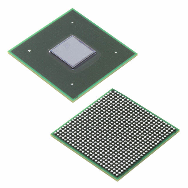


 工商网监
湘ICP备2023018690号
工商网监
湘ICP备2023018690号
