Document Number: MD7IC2012N
Rev. 0, 4/2013
Freescale Semiconductor
Technical Data
RF LDMOS Wideband Integrated
Power Amplifiers
The MD7IC2012N wideband integrated circuit is designed with on−chip
matching that makes it usable from 1805 to 2170 MHz. This multi−stage
structure is rated for 24 to 32 volt operation and covers all typical cellular
base station modulation formats.
Driver Application — 2100 MHz
• Typical Single−Carrier W−CDMA Performance: VDD = 28 Volts,
IDQ1A = IDQ1B = 20 mA, IDQ2A = IDQ2B = 70 mA, Pout = 1.3 Watts Avg.,
IQ Magnitude Clipping, Channel Bandwidth = 3.84 MHz, Input Signal
PAR = 7.5 dB @ 0.01% Probability on CCDF.
Frequency
Gps
(dB)
PAE
(%)
ACPR
(dBc)
2110 MHz
31.0
14.7
−51.3
2140 MHz
31.3
14.8
−51.2
2170 MHz
31.5
14.9
−50.6
• Capable of Handling 5:1 VSWR, @ 32 Vdc, 2140 MHz, 14 Watts CW
Output Power (3 dB Input Overdrive from Rated Pout)
• Typical Pout @ 1 dB Compression Point ] 12 Watts CW
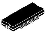
MD7IC2012NR1
MD7IC2012GNR1
1805−2170 MHz, 1.3 W AVG., 28 V
SINGLE W−CDMA
RF LDMOS WIDEBAND
INTEGRATED POWER AMPLIFIERS
TO−270 WB−14
PLASTIC
MD7IC2012NR1
TO−270 WB−14 GULL
PLASTIC
MD7IC2012GNR1
Driver Application — 1800 MHz
• Typical Single−Carrier W−CDMA Performance: VDD = 28 Volts,
IDQ1A = IDQ1B = 20 mA, IDQ2A = IDQ2B = 70 mA, Pout = 1.3 Watts Avg.,
IQ Magnitude Clipping, Channel Bandwidth = 3.84 MHz, Input Signal
PAR = 7.5 dB @ 0.01% Probability on CCDF.
Frequency
Gps
(dB)
PAE
(%)
ACPR
(dBc)
1805 MHz
32.8
13.4
−51.0
1840 MHz
32.2
13.6
−51.2
1880 MHz
31.6
13.8
−51.8
Features
•
•
•
•
•
•
•
•
Characterized with Series Equivalent Large−Signal Impedance Parameters and Common Source S−Parameters
On−Chip Matching (50 Ohm Input, DC Blocked)
Integrated Quiescent Current Temperature Compensation with Enable/Disable Function (1)
Integrated ESD Protection
Designed for Digital Predistortion Error Correction Systems
Optimized for Doherty Applications
225°C Capable Plastic Package
In Tape and Reel. R1 Suffix = 500 Units, 44 mm Tape Width, 13−inch Reel.
1. Refer to AN1977, Quiescent Current Thermal Tracking Circuit in the RF Integrated Circuit Family and to AN1987, Quiescent Current Control
for the RF Integrated Circuit Device Family. Go to http://www.freescale.com/rf. Select Documentation/Application Notes − AN1977 or AN1987.
© Freescale Semiconductor, Inc., 2013. All rights reserved.
RF Device Data
Freescale Semiconductor, Inc.
MD7IC2012NR1 MD7IC2012GNR1
1
�VDS1A
RFinA
VDS1A
VGS2A
VGS1A
RFinA
N.C.
N.C.
N.C.
N.C.
RFinB
VGS1B
VGS2B
VDS1B
RFout1/VDS2A
VGS1A
Quiescent Current
Temperature Compensation (1)
VGS2A
VGS1B
Quiescent Current
Temperature Compensation (1)
VGS2B
RFinB
1
2
3
4
5
6
7
8
9
10
11
12
14
13
RFout1/VDS2A
RFout2/VDS2B
(Top View)
RFout2/VDS2B
Note: Exposed backside of the package is
the source terminal for the transistors.
VDS1B
Figure 2. Pin Connections
Figure 1. Functional Block Diagram
Table 1. Maximum Ratings
Rating
Symbol
Value
Unit
Drain−Source Voltage
VDSS
−0.5, +65
Vdc
Gate−Source Voltage
VGS
−0.5, +10
Vdc
Operating Voltage
VDD
32, +0
Vdc
Storage Temperature Range
Tstg
−65 to +150
°C
TC
150
°C
Case Operating Temperature
Operating Junction Temperature
(2,3)
Input Power
TJ
225
°C
Pin
20
dBm
Symbol
Value (3,4)
Unit
Table 2. Thermal Characteristics
Characteristic
Thermal Resistance, Junction to Case
Case Temperature 77°C, 1.3 W, 2170 MHz
Stage 1, 28 Vdc, IDQ1A = IDQ1B = 20 mA, 2170 MHz
Stage 2, 28 Vdc, IDQ2A = IDQ2B = 70 mA, 2170 MHz
Case Temperature 79°C, 12 W CW, 2170 MHz
Stage 1, 28 Vdc, IDQ1A = IDQ1B = 20 mA, 2170 MHz
Stage 2, 28 Vdc, IDQ2A = IDQ2B = 70 mA, 2170 MHz
°C/W
RθJC
7.8
3.1
7.3
2.4
Table 3. ESD Protection Characteristics
Test Methodology
Class
Human Body Model (per JESD22−A114)
1A
Machine Model (per EIA/JESD22−A115)
A
Charge Device Model (per JESD22−C101)
II
Table 4. Moisture Sensitivity Level
Test Methodology
Per JESD22−A113, IPC/JEDEC J−STD−020
Rating
Package Peak Temperature
Unit
3
260
°C
1. Refer to AN1977, Quiescent Current Thermal Tracking Circuit in the RF Integrated Circuit Family and to AN1987, Quiescent Current Control
for the RF Integrated Circuit Device Family. Go to http://www.freescale.com/rf. Select Documentation/Application Notes − AN1977 or AN1987.
2. Continuous use at maximum temperature will affect MTTF.
3. MTTF calculator available at http://www.freescale.com/rf. Select Software & Tools/Development Tools/Calculators to access MTTF
calculators by product.
4. Refer to AN1955, Thermal Measurement Methodology of RF Power Amplifiers. Go to http://www.freescale.com/rf. Select
Documentation/Application Notes − AN1955.
MD7IC2012NR1 MD7IC2012GNR1
2
RF Device Data
Freescale Semiconductor, Inc.
�Table 5. Electrical Characteristics (TA = 25°C unless otherwise noted)
Symbol
Min
Typ
Max
Unit
Zero Gate Voltage Drain Leakage Current
(VDS = 65 Vdc, VGS = 0 Vdc)
IDSS
—
—
10
μAdc
Zero Gate Voltage Drain Leakage Current
(VDS = 28 Vdc, VGS = 0 Vdc)
IDSS
—
—
1
μAdc
Gate−Source Leakage Current
(VGS = 1.5 Vdc, VDS = 0 Vdc)
IGSS
—
—
1
μAdc
Gate Threshold Voltage
(VDS = 10 Vdc, ID = 5 μAdc)
VGS(th)
1.2
2.0
2.7
Vdc
Gate Quiescent Voltage
(VDS = 28 Vdc, IDQ1A = IDQ1B = 20 mA)
VGS(Q)
—
2.7
—
Vdc
Fixture Gate Quiescent Voltage
(VDD = 28 Vdc, IDQ1A = IDQ1B = 20 mA, Measured in Functional Test)
VGG(Q)
4.2
5.0
5.7
Vdc
Zero Gate Voltage Drain Leakage Current
(VDS = 65 Vdc, VGS = 0 Vdc)
IDSS
—
—
10
μAdc
Zero Gate Voltage Drain Leakage Current
(VDS = 28 Vdc, VGS = 0 Vdc)
IDSS
—
—
1
μAdc
Gate−Source Leakage Current
(VGS = 1.5 Vdc, VDS = 0 Vdc)
IGSS
—
—
1
μAdc
Gate Threshold Voltage
(VDS = 10 Vdc, ID = 24 μAdc)
VGS(th)
1.2
2.0
2.7
Vdc
Gate Quiescent Voltage
(VDS = 28 Vdc, IDQ2A = IDQ2B = 70 mA)
VGS(Q)
—
2.0
—
Vdc
Fixture Gate Quiescent Voltage
(VDD = 28 Vdc, IDQ2A = IDQ2B = 70 mA, Measured in Functional Test)
VGG(Q)
3.2
4.0
4.7
Vdc
Drain−Source On−Voltage
(VGS = 10 Vdc, ID = 200 mAdc)
VDS(on)
0.1
0.24
1.5
Vdc
Characteristic
Stage 1 − Off Characteristics (1)
Stage 1 − On Characteristics (1)
Stage 2 − Off Characteristics (1)
Stage 2 − On Characteristics (1)
Functional Tests (2,3) (In Freescale Test Fixture, 50 ohm system) VDD = 28 Vdc, IDQ1A = IDQ1B = 20 mA, IDQ2A = IDQ2B = 70 mA,
Pout = 1.3 W Avg., f = 2170 MHz, Single−Carrier W−CDMA, IQ Magnitude Clipping, Input Signal PAR = 7.5 dB @ 0.01% Probability on CCDF.
ACPR measured in 3.84 MHz Channel Bandwidth @ ±5 MHz Offset.
Gps
30.7
31.5
34.7
Power Added Efficiency
PAE
13.2
14.9
—
%
Output Peak−to−Average Ratio @ 0.01% Probability on CCDF
PAR
6.8
7.3
—
dB
ACPR
—
−50.6
−48.3
dBc
Power Gain
Adjacent Channel Power Ratio
dB
1. Each side of device measured separately.
2. Part internally matched both on input and output.
3. Measurement made with device in straight lead configuration before any lead forming operation is applied. Lead forming is used for gull
wing (GN) parts.
(continued)
MD7IC2012NR1 MD7IC2012GNR1
RF Device Data
Freescale Semiconductor, Inc.
3
�Table 5. Electrical Characteristics (TA = 25°C unless otherwise noted) (continued)
Characteristic
Symbol
Min
Typ
Max
Unit
Typical Performance (In Freescale Test Fixture, 50 ohm system) VDD = 28 Vdc, IDQ1A = IDQ1B = 20 mA, IDQ2A = IDQ2B = 70 mA,
2110−2170 MHz Bandwidth
Pout @ 1 dB Compression Point, CW
P1dB
—
12
—
W
Pout @ 3 dB Compression Point, CW
P3dB
—
13
—
W
—
60
—
—
85
—
—
—
2.5
2.5
—
—
IMD Symmetry @ 10 W PEP, Pout where IMD Third Order
Intermodulation ` 30 dBc
(Delta IMD Third Order Intermodulation between Upper and Lower
Sidebands > 2 dB)
IMDsym
VBW Resonance Point
(IMD Third Order Intermodulation Inflection Point)
VBWres
Quiescent Current Accuracy over Temperature (1,2)
with 2 kΩ Gate Feed Resistors (−30 to 85°C)
with 2 kΩ Gate Feed Resistors (−30 to 85°C)
MHz
ΔIQT
Stage 1
Stage 2
MHz
%
Gain Flatness in 60 MHz Bandwidth @ Pout = 1.3 W Avg.
GF
—
0.2
—
dB
Gain Variation over Temperature
(−30°C to +85°C)
ΔG
—
0.03
—
dB/°C
ΔP1dB
—
0.012
—
dB/°C
Output Power Variation over Temperature
(−30°C to +85°C)
1. Each side of device measured separately.
2. Refer to AN1977, Quiescent Current Thermal Tracking Circuit in the RF Integrated Circuit Family and to AN1987, Quiescent Current Control for
the RF Integrated Circuit Device Family. Go to http://www.freescale.com/rf. Select Documentation/Application Notes − AN1977 or AN1987.
MD7IC2012NR1 MD7IC2012GNR1
4
RF Device Data
Freescale Semiconductor, Inc.
�VGG1A
VGG2A
R1
R2
VDD1A
V
C32 DD2A
C31
C24
C23
MD7IC2012N
Rev. 2
C2
C25
C1
C17
C19
C29
C36
C35
R6
C5
C6
C9
C10
C13 C15
C14 C16
Z1
C8
C7
C37
C38
C12
C20
C3
C28
C4
R3
R4
C27
VGG1B
VGG2B
Z2
C11
CUT OUT AREA
R5
C26
C21
C22
C30
C18
C33
VDD1B
C34
VDD2B
Figure 3. MD7IC2012NR1 Test Circuit Component Layout — 1805−2170 MHz
Table 6. MD7IC2012NR1 Test Circuit Component Designations and Values — 1805−2170 MHz
Part
Description
Part Number
Manufacturer
C1, C2, C3, C4
3.9 pF Chip Capacitors
ATC600F3R9BT250XT
ATC
C5, C6, C7, C8
1.0 pF Chip Capacitors
ATC600F1R0BT250XT
ATC
C9, C10, C11, C12
0.6 pF Chip Capacitors
ATC600F0R6BT250XT
ATC
C13, C14
0.8 pF Chip Capacitors
ATC600F0R8BT250XT
ATC
C15, C16
1.2 pF Chip Capacitors
ATC600F1R2BT250XT
ATC
C17, C18, C19, C20
10 pF Chip Capacitors
ATC600F10RBT250XT
ATC
C21, C22
5.6 pF Chip Capacitors
ATC600F5R6BT250XT
ATC
C23, C24, C25, C26, C27, C28,
C29, C30, C31, C32, C33, C34
10 mF, Chip Capacitors
C5750X7S2A106M230KB
TDK
C35, C36, C37, C38
22 nF Chip Capacitors
GRM31BR72E223KW01L
Murata
R1, R2, R3, R4
2 kW, 1/8 W Chip Resistors
CRCW12062K00FKEA
Vishay
R5, R6
50 W, 20 W SM Chip Power Resistors
C20N50Z4
Anaren
Z1, Z2
1800−2300 MHz Band, 90°, 3 dB Hybrid Coupler
X3C21P1−03S
Anaren
PCB
0.020″, er = 3.50
RO4350B
Rogers
MD7IC2012NR1 MD7IC2012GNR1
RF Device Data
Freescale Semiconductor, Inc.
5
�15
14
Single-Carrier W-CDMA, 3.84 MHz Channel Bandwidth 13
Input Signal PAR = 7.5 dB @ 0.01% Probability on CCDF
12
33
32.5
32
Gps
31.5
31
PARC
ACPR
30.5
-47
0.4
-48
0.3
-49
30
-50
29.5
-51
29
1800
1850
1900
1950
2000
2050
2100
2150
0.2
0.1
PARC (dB)
33.5
Gps, POWER GAIN (dB)
16
VDD = 28 Vdc, Pout = 1.3 W (Avg.), IDQ1A = IDQ1B = 20 mA
IDQ2A = IDQ2B = 70 mA
PAE
ACPR (dBc)
34
PAE, POWER ADDED
EFFICIENCY (%)
TYPICAL CHARACTERISTICS — 1805−2170 MHz
-0
-52
2200
-0.1
f, FREQUENCY (MHz)
IMD, INTERMODULATION DISTORTION (dBc)
Figure 4. Output Peak−to−Average Ratio Compression (PARC)
Broadband Performance @ Pout = 1.3 Watts Avg.
-20
VDD = 28 Vdc, IDQ1A = IDQ1B = 20 mA
IDQ2A = IDQ2B = 70 mA, Pout = 10 W (PEP)
IM3-U
-30
IM3-L
-40
IM5-U
IM5-L
-50
IM7-U
-60
IM7-L
Two-Tone Measurements
(f1 + f2)/2 = Center Frequency of 2140 MHz
-70
10
1
100
TWO-TONE SPACING (MHz)
Figure 5. Intermodulation Distortion Products
versus Two−Tone Spacing
30
29
28
27
0
50
Gps
-1
40
-1 dB = 3.1 W
-2
-2 dB = 4.2 W
PAE
-3
30
ACPR
-4
20
PARC
-3 dB = 5 W
3.84 MHz Channel Bandwidth
Input Signal PAR = 7.5 dB @ 0.01% Probability on CCDF
-5
1
2
3
4
5
10
0
-25
-30
-35
ACPR (dBc)
31
OUTPUT COMPRESSION AT 0.01%
PROBABILITY ON CCDF (dB)
Gps, POWER GAIN (dB)
32
-20
60
VDD = 28 Vdc, IDQ1A = IDQ1B = 20 mA, IDQ2A = IDQ2B = 70 mA
f = 2140 MHz, Single-Carrier W-CDMA
PAE, POWER ADDED EFFICIENCY (%)
1
33
-40
-45
-50
6
Pout, OUTPUT POWER (WATTS)
Figure 6. Output Peak−to−Average Ratio
Compression (PARC) versus Output Power
MD7IC2012NR1 MD7IC2012GNR1
6
RF Device Data
Freescale Semiconductor, Inc.
�TYPICAL CHARACTERISTICS — 1805−2170 MHz
0
31 1800 MHz
30
Gps
ACPR
2000 MHz
2200 MHz
2200 MHz
2000 MHz
29
1800 MHz
10
1
20
10
PAE, POWER ADDED EFFICIENCY (%)
Gps, POWER GAIN (dB)
30
32
0
-10
-20
-30
-40
ACPR (dBc)
60
VDD = 28 Vdc, IDQ1A = IDQ1B = 20 mA, IDQ2A = IDQ2B = 70 mA
Single-Carrier W-CDMA, 3.84 MHz Channel
2000 MHz 50
34 Bandwidth, Input Signal PAR = 7.5 dB @ 0.01%
Probability on CCDF
1800 MHz
PAE
33
40
2200 MHz
35
-50
-60
20
Pout, OUTPUT POWER (WATTS) AVG.
Figure 7. Single−Carrier W−CDMA Power Gain,
Power Added Efficiency and ACPR versus Output Power
42
38
Gain
GAIN (dB)
34
30
26
VDD = 28 Vdc
IDQ1A = IDQ1B = 20 mA
IDQ2A = IDQ2B = 70 mA
Pin = 0 dBm
22
18
1450
1600
1750
1900
2050
2200
2350
2500
2650
f, FREQUENCY (MHz)
Figure 8. Broadband Frequency Response
MD7IC2012NR1 MD7IC2012GNR1
RF Device Data
Freescale Semiconductor, Inc.
7
�W−CDMA TEST SIGNAL
100
10
0
-10
3.84 MHz
Channel BW
-20
1
Input Signal
-30
0.1
(dB)
PROBABILITY (%)
10
0.01
W-CDMA. ACPR Measured in 3.84 MHz
Channel Bandwidth @ ±5 MHz Offset.
Input Signal PAR = 7.5 dB @ 0.01%
Probability on CCDF
0.001
0.0001
0
1
2
3
4
5
6
-40
-50
-60
+ACPR in 3.84 MHz
Integrated BW
-ACPR in 3.84 MHz
Integrated BW
-70
-80
7
8
9
PEAK-TO-AVERAGE (dB)
Figure 9. CCDF W−CDMA IQ Magnitude
Clipping, Single−Carrier Test Signal
10
-90
-100
-9
-7.2 -5.4 -3.6 -1.8
0
1.8
3.6
5.4
7.2
9
f, FREQUENCY (MHz)
Figure 10. Single−Carrier W−CDMA Spectrum
MD7IC2012NR1 MD7IC2012GNR1
8
RF Device Data
Freescale Semiconductor, Inc.
�VDD = 28 Vdc, IDQ1A = IDQ1B = 20 mA, IDQ2A = IDQ2B = 70 mA, Pout = 1.3 W Avg.
f
MHz
Zin
W
Zload
W
1800
73.3 + j2.21
7.94 − j1.22
1850
82.5 − j7.53
8.26 − j0.97
1900
80.1 − j27.0
8.40 − j1.13
1950
73.8 − j29.4
8.55 − j2.03
2000
64.6 − j33.8
8.67 − j2.62
2050
55.8 − j28.6
8.85 − j2.62
2100
50.5 − j27.2
8.64 − j2.79
2150
50.5 − j27.2
8.43 − j2.89
45.7 − j19.8
8.05 − j2.95
2200
Zin
=
Zload =
Device input impedance as measured from
gate to ground.
Test circuit impedance as measured from
drain to ground.
Output
Matching
Network
Device
Under
Test
Zin
Zload
Figure 11. Series Equivalent Input and Load Impedance — 1805−2170 MHz
MD7IC2012NR1 MD7IC2012GNR1
RF Device Data
Freescale Semiconductor, Inc.
9
�VDD = 28 Vdc, IDQ1A = 12 mA, IDQ2A = 80 mA, CW
Max Output Power
P1dB
f
(MHz)
Zsource
(W)
Zin
(W)
Zload (1)
(W)
Gain (dB)
(dBm)
(W)
hD
(%)
AM/PM
(5)
2110
48.7 + j29.5
46.6 − j28.5
8.66 − j3.87
28.2
40.0
10.0
50.8
−5.3
2140
46.8 + j28.4
43.5 − j25.5
7.73 − j3.91
28.8
40.0
10.0
52.7
−7.2
2170
44.5 + j20.1
42.5 − j22.4
7.57 − j4.37
29.0
40.0
10.0
52.7
−6.9
Max Output Power
P3dB
f
(MHz)
Zsource
(W)
Zin
(W)
Zload
(W)
Gain (dB)
(dBm)
(W)
hD
(%)
AM/PM
(5)
(2)
2110
48.7 + j29.5
46.3 + j26.5
8.66 − j3.87
26.2
40.7
11.8
51.6
−7.9
2140
46.8 + j28.4
43.9 − j22.5
9.01 − j4.25
26.4
40.7
11.8
50.8
−9.4
2170
44.5 + j20.1
42.9 − j19.4
8.73 − j4.51
26.6
40.7
11.8
51.2
−9.2
(1) Load impedance for optimum P1dB power. (2) Load impedance for optimum P3dB power.
Zsource = Measured impedance presented to the input of the device at the package reference plane.
Zin
= Impedance as measured from gate contact to ground.
Zload = Measured impedance presented to the output of the device at the package reference plane.
Note: Measurement made on a per side basis.
Figure 12. Load Pull Performance — Maximum Power Tuning
VDD = 28 Vdc, IDQ1A = 12 mA, IDQ2A = 80 mA, CW
Max Power Added Efficiency
P1dB
f
(MHz)
Zsource
(W)
Zin
(W)
Zload (1)
(W)
Gain (dB)
(dBm)
(W)
hD
(%)
AM/PM
(5)
2110
48.7 + j29.5
43.2 − j34.5
4.39 − j1.83
30.0
38.8
7.5
57.7
−12
2140
46.8 + j28.4
40.9 − j30.0
4.39 − j2.52
30.4
38.9
7.7
57.2
−13
2170
44.5 + j20.1
39.6 − j25.9
4.69 − j2.49
30.5
38.9
7.8
56.9
−12
Max Power Added Efficiency
P3dB
f
(MHz)
Zsource
(W)
Zin
(W)
Zload
(W)
Gain (dB)
(dBm)
(W)
hD
(%)
AM/PM
(5)
(2)
2110
48.7 + j29.5
44.3 − j30.6
5.17 − j2.00
27.7
39.7
9.4
56.5
−12
2140
46.8 + j28.4
41.8 − j25.9
5.53 − j2.22
27.9
39.8
9.6
56.1
−13
2170
44.5 + j20.1
40.2 − j23.7
4.69 − j2.49
28.4
39.4
8.7
55.7
−14
(1) Load impedance for optimum P1dB efficiency (2) Load impedance for optimum P3dB efficiency.
Zsource = Measured impedance presented to the input of the device at the package reference plane.
Zin
= Impedance as measured from gate contact to ground.
Zload = Measured impedance presented to the output of the device at the package reference plane.
Note: Measurement made on a per side basis.
Figure 13. Load Pull Performance — Maximum Power Added Efficiency Tuning
Output Load Pull
Tuner and
Test Circuit
Device
Under
Test
Zin
Zload
MD7IC2012NR1 MD7IC2012GNR1
10
RF Device Data
Freescale Semiconductor, Inc.
�VDD = 28 Vdc, IDQ1A = 12 mA, IDQ2A = 80 mA, CW
Max Output Power
P1dB
f
(MHz)
Zsource
(W)
Zin
(W)
Zload (1)
(W)
Gain (dB)
(dBm)
(W)
hD
(%)
AM/PM
(5)
1805
61.8 − j5.85
61.6 + j7.80
8.04 − j0.206
29.6
40.0
10.0
54.7
−11
1840
73.7 − j4.41
70.3 + j1.44
8.01 − j0.273
29.8
40.0
10.0
55.9
−7.6
1880
73.3 + 8.94
74.5 − j7.06
8.65 − j1.23
29.2
40.0
10.0
53.8
−6.9
Max Output Power
P3dB
Gain (dB)
(dBm)
(W)
hD
(%)
AM/PM
(5)
8.65 − j0.359
27.4
40.7
11.7
55.4
−18
9.34 − j0.874
27.3
40.7
11.7
54.7
−13
8.65 − j1.23
27.2
40.8
12.0
55.5
−10
Zload
(W)
f
(MHz)
Zsource
(W)
Zin
(W)
1805
61.8 − j5.85
61.7 + j5.98
1840
73.7 − j4.41
67.7 − j0.606
1880
73.3 + j8.94
72.8 − j7.46
(2)
(1) Load impedance for optimum P1dB power. (2) Load impedance for optimum P3dB power.
Zsource = Measured impedance presented to the input of the device at the package reference plane.
Zin
= Impedance as measured from gate contact to ground.
Zload = Measured impedance presented to the output of the device at the package reference plane.
Note: Measurement made on a per side basis.
Figure 14. Load Pull Performance — Maximum Power Tuning
VDD = 28 Vdc, IDQ1A = 12 mA, IDQ2A = 80 mA, CW
Max Power Added Efficiency
P1dB
f
(MHz)
Zsource
(W)
Zin
(W)
Zload (1)
(W)
Gain (dB)
(dBm)
(W)
hD
(%)
AM/PM
(5)
1805
61.8 − j5.85
69.9 + j14.4
5.10 + j2.07
31.4
38.9
7.8
60.8
−13
1840
73.7 − j4.41
81.0 + j0.271
5.52 + j2.11
31.6
38.8
7.6
60.3
−9.1
1880
73.3 + j8.94
87.3 − j10.7
4.69 + j0.912
31.0
38.9
7.8
61.1
−10
Max Power Added Efficiency
P3dB
Gain (dB)
(dBm)
(W)
hD
(%)
AM/PM
(5)
5.05 - j0.32
29.3
39.6
9.3
61.4
-15
5.52 + j2.11
29.6
39.5
9.3
61.3
-11
28.8
39.8
9.3
61.4
-12
Zload
(W)
(2)
f
(MHz)
Zsource
(W)
Zin
(W)
1805
61.8 - j5.85
68.1 + j8.57
1840
73.7 - j4.41
76.4 - j1.31
1880
73.3 + j8.94
79.4 - j10.8
5.43 + j1.07
(1) Load impedance for optimum P1dB efficiency (2) Load impedance for optimum P3dB efficiency.
Zsource = Measured impedance presented to the input of the device at the package reference plane.
Zin
= Impedance as measured from gate contact to ground.
Zload = Measured impedance presented to the output of the device at the package reference plane.
Note: Measurement made on a per side basis.
Figure 15. Load Pull Performance — Maximum Power Added Efficiency Tuning
Output Load Pull
Tuner and
Test Circuit
Device
Under
Test
Zin
Zload
MD7IC2012NR1 MD7IC2012GNR1
RF Device Data
Freescale Semiconductor, Inc.
11
�PACKAGE DIMENSIONS
MD7IC2012NR1 MD7IC2012GNR1
12
RF Device Data
Freescale Semiconductor, Inc.
�MD7IC2012NR1 MD7IC2012GNR1
RF Device Data
Freescale Semiconductor, Inc.
13
�MD7IC2012NR1 MD7IC2012GNR1
14
RF Device Data
Freescale Semiconductor, Inc.
�MD7IC2012NR1 MD7IC2012GNR1
RF Device Data
Freescale Semiconductor, Inc.
15
�MD7IC2012NR1 MD7IC2012GNR1
16
RF Device Data
Freescale Semiconductor, Inc.
�MD7IC2012NR1 MD7IC2012GNR1
RF Device Data
Freescale Semiconductor, Inc.
17
�PRODUCT DOCUMENTATION, SOFTWARE AND TOOLS
Refer to the following documents, software and tools to aid your design process.
Application Notes
• AN1907: Solder Reflow Attach Method for High Power RF Devices in Over−Molded Plastic Packages
• AN1955: Thermal Measurement Methodology of RF Power Amplifiers
• AN1977: Quiescent Current Thermal Tracking Circuit in the RF Integrated Circuit Family
• AN1987: Quiescent Current Control for the RF Integrated Circuit Device Family
• AN3789: Clamping of High Power RF Transistors and RFICs in Over−Molded Plastic Packages
Engineering Bulletins
• EB212: Using Data Sheet Impedances for RF LDMOS Devices
Software
• Electromigration MTTF Calculator
• RF High Power Model
• .s2p File
Development Tools
• Printed Circuit Boards
For Software and Tools, do a Part Number search at http://www.freescale.com, and select the “Part Number” link. Go to the
Software & Tools tab on the part’s Product Summary page to download the respective tool.
REVISION HISTORY
The following table summarizes revisions to this document.
Revision
Date
0
Apr. 2013
Description
• Initial Release of Data Sheet
MD7IC2012NR1 MD7IC2012GNR1
18
RF Device Data
Freescale Semiconductor, Inc.
�How to Reach Us:
Home Page:
freescale.com
Web Support:
freescale.com/support
Information in this document is provided solely to enable system and software
implementers to use Freescale products. There are no express or implied copyright
licenses granted hereunder to design or fabricate any integrated circuits based on the
information in this document.
Freescale reserves the right to make changes without further notice to any products
herein. Freescale makes no warranty, representation, or guarantee regarding the
suitability of its products for any particular purpose, nor does Freescale assume any
liability arising out of the application or use of any product or circuit, and specifically
disclaims any and all liability, including without limitation consequential or incidental
damages. “Typical” parameters that may be provided in Freescale data sheets and/or
specifications can and do vary in different applications, and actual performance may
vary over time. All operating parameters, including “typicals,” must be validated for
each customer application by customer’s technical experts. Freescale does not convey
any license under its patent rights nor the rights of others. Freescale sells products
pursuant to standard terms and conditions of sale, which can be found at the following
address: freescale.com/SalesTermsandConditions.
Freescale and the Freescale logo are trademarks of Freescale Semiconductor, Inc.,
Reg. U.S. Pat. & Tm. Off. All other product or service names are the property of their
respective owners.
E 2013 Freescale Semiconductor, Inc.
MD7IC2012NR1 MD7IC2012GNR1
Document
Number:
RF
Device
Data MD7IC2012N
Rev. 0, 4/2013Semiconductor, Inc.
Freescale
19
�


 工商网监
湘ICP备2023018690号
工商网监
湘ICP备2023018690号
