Freescale Semiconductor, Inc.
Product Brief
MPC533PB/D
Rev. 0, 2/2003
Freescale Semiconductor, Inc...
MPC533/MPC534
Product Brief
This document provides an overview of the MPC533/MPC534 microcontroller, including a
block diagram showing the major modular components, sections that list the major features,
and differences between the MPC533 and the MPC555. The MPC533 and MPC534 devices
are members of the Motorola MPC500 RISC Microcontroller family. The parts herein will be
referred to only as MPC533 unless specific parts need to be referenced.
Table 1. MPC533/MPC534 Features
1
Device
Flash
Code Compression
MPC533
512 Kbytes
Code compression not supported
MPC534
512 Kbytes
Code compression supported
Introduction
The MPC533 device offers the following features:
•
•
•
•
32-bit single issue PowerPC™ core
Unified system integration unit (USIU) with a flexible memory controller and
enhanced interrupt controller (EIC)
64-bit floating-point unit (FPU)
512-Kbytes of Flash EEPROM memory
— Typical endurance of 100,000 write/erase cycles @ 25ºC
— Typical data retention of 100 years @ 25ºC
•
•
•
•
•
•
32-Kbytes of static RAM in one CALRAM module, configured as
— 28-Kbyte normal access only array
— 4-Kbyte normal access or overlay access array (eight 512-byte regions)
One 22-timer channel modular I/O system (MIOS14)
One TouCAN module (TouCAN B)
Enhanced queued analog system (QADC64E)
One queued serial multi-channel module (QSMCM), which contains one queued
serial peripheral interface (QSPI) and two serial controller interfaces (SCI/UART)
One peripheral pin multiplexing module (PPM) with a parallel to serial driver
For More Information On This Product,
Go to: www.freescale.com
�Block Diagram
•
•
Freescale Semiconductor, Inc...
•
•
•
1.1
Freescale Semiconductor, Inc.
Debug features:
— Nexus debug port (Level 3)
— Background debug mode (BDM)
— IEEE1194.1 compliant interface (JTAG)
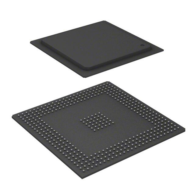
Plastic ball grid array (PBGA) packaging
— 388 ball PBGA
— 27 mm x 27 mm body size
— 1.0 mm ball pitch
40-MHz operation
-40°C–85°C
Two power supplies
— 5-V I/O (5.0 ± 0.25 V)
— 2.6 ± 0.1-V external bus with a 5-V tolerant I/O system
— 2.6 ± 0.1-V internal logic
— IRAMSTBY on-chip voltage regulator
Block Diagram
Figure 1 is a block diagram of the MPC533.
2
MPC533/MPC534 Product Brief
For More Information On This Product,
Go to: www.freescale.com
MOTOROLA
�Freescale Semiconductor, Inc.
Key Features
512 Kbytes
Flash
JTAG
Burst
Buffer
Controller
U-Bus
E-Bus
USIU
Freescale Semiconductor, Inc...
PowerPC
Core
+
FPU
READI
L2U
L-Bus
32-Kbyte CALRAM
28-Kbyte
SRAM
(No Overlay)
4-Kbyte Overlay
QSMCM
UIMB
PPM
IMB3
QADC64E
Tou
CAN
MIOS14
Figure 1. MPC533 Block Diagram
1.2
Key Features
The MPC533 key features are explained in the following sections.
1.2.1
•
•
High Performance CPU System
Fully static design
Four major power saving modes
— On, doze, sleep, deep-sleep, and power-down
MOTOROLA
MPC533/MPC534 Product Brief
For More Information On This Product,
Go to: www.freescale.com
3
�Key Features
1.2.1.1
•
•
•
•
Freescale Semiconductor, Inc...
•
•
•
•
•
•
•
•
4
MPC500 System Interface (USIU)
System configuration and protection features:
— Periodic-interrupt timer
— Bus monitor
— Software watchdog timer
— Real-time clock (RTC)
— PPC decrementer
— Time base
Clock synthesizer
Power management
Reset controller
External bus interface that tolerates 5-V inputs, provides 2.6-V outputs, and supports
multiple-master designs
Enhanced interrupt controller that supports up to eight external and 40 internal interrupts,
simplifies the interrupt structure, and decreases interrupt processing time
USIU supports dual mapping to map part of one internal/external memory to another external
memory
External bus, supporting non-wraparound burst for instruction fetches, with up to 8 instructions
per memory cycle
1.2.1.3
•
•
•
•
RISC MCU Central Processing Unit (RCPU)
32-bit single issue PowerPC core
Precise exception model
64-bit floating point unit (FPU)
Code compression supported on MPC534
— Reduces usage of internal/external Flash memory (up to 50% for code)
— The code compression feature is optimized for automotive (non-cached) applications
Extensive system development support
— On-chip watchpoints and breakpoints
— Program flow tracking
1.2.1.2
•
Freescale Semiconductor, Inc.
Burst Buffer Controller (BBC) Module
Support for enhanced interrupt controller (EIC)
Support for enhanced exception table relocation feature
Branch target buffer
Contains 2 Kbytes of decompression RAM (DECRAM) for code compression. This RAM may
also be used as general-purpose RAM when code compression feature not used.
MPC533/MPC534 Product Brief
For More Information On This Product,
Go to: www.freescale.com
MOTOROLA
�Freescale Semiconductor, Inc.
1.2.1.4
•
•
•
•
Freescale Semiconductor, Inc...
•
•
•
•
32-Kbyte Static RAM (CALRAM)
Composed of one 32-Kbyte CALRAM module
— 28-Kbyte static RAM
— 4-Kbyte calibration (overlay) RAM feature that allows calibration of flash-based constants
Eight 512-byte overlay regions
One clock fast accesses
Two clock cycle access option for power saving
Keep-alive power (IRAMSTBY) for data retention
1.2.1.8
•
•
•
•
•
512-Kbytes of CDR3 Flash EEPROM Memory (UC3F)
One 512-Kbyte module
Page read mode
Block (64 Kbytes) erasable
External 4.75- to 5.25-V VFLASH power supply for program, erase, and read operations
Typical endurance of 100,000 write/erase cycles @ 25ºC
Typical data retention of 100 years @ 25ºC
1.2.1.7
•
Memory Controller
Four flexible chip selects via memory controller
24-bit address and 32-bit data buses
4-Kbyte to one 16-Mbyte (data) or 4-Gbyte (instruction) region size support
Supports enhanced external burst
Up to eight-beat transfer bursts, two-clock minimum bus transactions
Use with SRAM, EPROM, flash and other peripherals
Byte selects or write enables
32-bit address decodes with bit masks
Four regions
1.2.1.6
•
•
•
•
•
•
Flexible Memory Protection Unit
Flexible memory protection units (MPU) in BBC and L2U
Default attributes available in one global entry
Attribute support for speculative accesses
Up to eight memory regions are supported, four for data and four for instructions
1.2.1.5
•
•
•
•
•
•
•
•
•
Key Features
General Purpose I/O Support (GPIO)
24 address pins and 32 data pins can be used for general-purpose I/O in single-chip mode
16 GPIO in MIOS14
Many peripheral pins can be used as GPIO when not used as primary functions
2.6-V outputs on external bus pins
5-V outputs with slew rate control
MOTOROLA
MPC533/MPC534 Product Brief
For More Information On This Product,
Go to: www.freescale.com
5
�Key Features
1.2.2
Freescale Semiconductor, Inc...
•
•
•
•
•
•
•
•
•
•
•
Nexus Debug Port (Class 3)
Compliant with Class 3 of the IEEE-ISTO 5001-1999
Program trace via branch trace messaging (BTM)
Data trace via data write messaging (DWM) and data read messaging (DRM)
Ownership trace via ownership trace messaging (OTM)
Run-time access to on-chip memory map and special purpose registers (SPRs) via the READI
read/write access protocol
Watchpoint messaging via the auxiliary port
9 or 16 full-duplex auxiliary pin interface for medium and high visibility throughput
All features configurable and controllable via the auxiliary port
Security features for production environment
Supports the RCPU debug mode via the auxiliary port
READI module can be reset independent of system reset
1.2.3
Integrated I/O System
1.2.3.1
•
•
•
•
•
•
•
•
•
•
•
•
•
•
•
6
22-Channel Modular I/O System (MIOS14)
Six modulus counter sub-modules (MCSM)
10 double-action sub-modules (DASM)
12 dedicated PWM sub-modules (PWMSM)
One MIOS14 16-bit parallel port I/O sub-modules (MPIOSM)
1.2.3.2
•
Freescale Semiconductor, Inc.
Enhanced Queued Analog-to-Digital Converter Module
(QADC64E)
Queued analog-to-digital converter module (QADC64E_A) providing a total of 16 analog
channels using internal multiplexing
Directly supports up to four external multiplexers
Up to 41 total input channels on the QADC64E module with external multiplexing
Software configurable to operate in enhanced or legacy (MPC555 compatible) mode
Unused analog channels can be used as digital input/output pins
GPIO on all channels in enhanced mode
10-bit A/D converter with internal sample/hold
Typical conversion time of less than 5 µs (>200 K samples/second)
Two conversion command queues of variable length
Automated queue modes initiated by:
— External edge trigger
— Software command
— Periodic/interval timer within QADC64E module, that can be assigned to both queue 1 and 2
— External gated trigger (queue 1 only)
64 result registers
— Output data is right- or left-justified, signed or unsigned.
Alternate reference input (ALTREF), with control in the conversion command word (CCW)
MPC533/MPC534 Product Brief
For More Information On This Product,
Go to: www.freescale.com
MOTOROLA
�Freescale Semiconductor, Inc.
1.2.3.3
Freescale Semiconductor, Inc...
•
•
•
•
•
•
Queued Serial Multi-Channel Module (QSMCM)
One queued serial module with one queued SPI and two SCIs (QSMCM)
QSMCM matches full MPC555 QSMCM functionality
Queued SPI
— Provides full-duplex communication port for peripheral expansion or inter-processor
communication
— Up to 32 preprogrammed transfers, reducing overhead
— Synchronous serial interface with baud rate of up to system clock / 4
— Four programmable peripheral-selects pins:
— Support up to 16 devices with external decoding
— Support up to eight devices with internal decoding
— Special wrap-around mode allows continuous sampling of a serial peripheral for efficient
interfacing to serial analog-to-digital (A/D) converters
SCI
— UART mode provides NRZ format and half- or full-duplex interface
— 16 register receive buffers and 16 register transmit buffers on one SCI
— Advanced error detection and optional parity generation and detection
— Word-length programmable as eight or nine bits
— Separate transmitter and receiver enable bits, and double buffering of data
— Wake-up functions allow the CPU to run uninterrupted until either a true idle line is detected,
or a new address byte is received
1.2.3.5
•
•
One CAN 2.0B Controller (TouCAN) Module
One TouCAN module (TouCAN B)
TouCAN provides the following features:
— 16 message buffers, programmable I/O modes
— Maskable interrupts
— Independent of the transmission medium (external transceiver is assumed)
— Open network architecture, multi-master concept
— High immunity to EMI
— Short latency time for high-priority messages
— Low-power sleep mode, with programmable wake-up on bus activity
1.2.3.4
•
•
•
Key Features
Peripheral Pin Multiplexing (PPM)
Synchronous serial interface between the microprocessor and an external device
Two internal parallel data sources can be multiplexed through the PPM
— MIOS14: 12 PWM channels, four MDA channels
— Internal GPIO: 16 general-purpose inputs, 16 general-purpose outputs
Software configurable stream size
Software configurable clock (TCLK) based on system clock
Software selectable clock modes (SPI mode and TDM mode)
MOTOROLA
MPC533/MPC534 Product Brief
For More Information On This Product,
Go to: www.freescale.com
7
�Freescale Semiconductor, Inc.
MPC533 Optional Features
•
Software selectable operation modes
— Continuous mode
— Start-transmit-receive (STR) mode
Software configurable internal modules interconnect (shorting)
•
1.3
MPC533 Optional Features
The following features of the MPC533 are optional features and may not appear in certain configurations:
•
Freescale Semiconductor, Inc...
2
Code compression on MPC534
Comparison of MPC533 and MPC555
The MPC533 is a derivative of the MPC555. Most functional features of the MPC555 are unchanged on the
MPC533. Refer to Table 2 for a comparison of features.
Table 2. Differences Between MPC555 and MPC533
Module
MPC555
MPC533
CPU Core
BBC
Identical
Basic
Enhanced Code Compression (classes scheme
with 2 Kbytes DECRAM)
Code Compression is available only on
MPC534.
L2U
Identical
SRAM
26 Kbytes
32 Kbytes calibration SRAM with overlay
features
Flash
448-Kbyte CMF
(2 modules, 256-Kbyte and 192-Kbyte)
512-Kbyte UC3F (1 module)
USIU
Basic
Enhanced Interrupt Controller
JTAG
Selectable by RCW
Selectable at PORESET
READI
None
New Debut Module (Class 3 Nexus
IEEE-ISTO 5001-1999)
UIMB
QADC64
Identical
(2)
QSMCM
MIOS
(1) Identical (1)
MIOS1
TouCAN
PPM
8
(1) Enhanced
MIOS14
4 Extra PWMSM
4 Extra MCSM
no Real-Time Clock
(2) Identical (1)
—
MPC533/MPC534 Product Brief
For More Information On This Product,
Go to: www.freescale.com
New Module
MOTOROLA
�Freescale Semiconductor, Inc.
Additional MPC533 Differences
2.1
•
•
Freescale Semiconductor, Inc...
•
•
•
•
•
•
•
•
Additional MPC533 Differences
The MPC533 is very similar to the MPC555 with the following differences:
— CDR3 technology
— Two power supplies: 5.0-V I/O, 2.6-V external bus pins, 2.6-V internal logic
— New modules: READI, CALRAM, PPM
— One less TouCAN module, 6 Kbytes extra of SRAM on L-bus (32 Kbytes total) (with
CALRAM overlay features)
QADC64
— GPO on all channel pins in addition to GPI functions
TouCAN, QSMCM, UIMB, Core, L2U
— No changes
BBC
— Enhanced interrupt controller support
— Enhanced exception relocation table
— Branch target buffer
— 2 Kbytes of decompression RAM for code compression. This may also be used as
general-purpose RAM while not used for code compression.
CALRAM (with overlay features)
— New module
— Overlay features allow calibration of Flash-based constants
UC3F (U-bus CDR3 Flash module)
— 512 Kbytes of non-volatile memory (NVM)
— Designed for use in embedded microcontroller (MCU) applications targeted for high speed
read performance and high density byte count requirements
READI
— New module
USIU
— Enhanced interrupt controller
— ENGCLK default frequency
— READI support
— Reduced data setup time
— Enhanced external burst support
MIOS14
— Four additional PWM channels
— Four additional MCSM timers
PPM (peripheral pin multiplexing)
— New module
— Two-to-one multiplexing
— Parallel to serial (SPI and TDM)
MOTOROLA
MPC533/MPC534 Product Brief
For More Information On This Product,
Go to: www.freescale.com
9
�Freescale Semiconductor, Inc.
Additional MPC533 Differences
3
SRAM Keep-Alive Power Behavior
One keep-alive power pin (IRAMSTBY) provides keep-alive power to RAM.
The IRAMSTBY pin can be powered directly from a battery using an internal shunt regulator or via a small
battery for standby use. See Figure 2.
To Battery
R
To IRAMSTBY Pad
Freescale Semiconductor, Inc...
C
Figure 2. Recommended Connection Diagram for IRAMSTBY
While power is off to the MPC533, the IRAMSTBY supply powers the following:
•
•
4
32-Kbyte CALRAM
2-Kbyte BBC DECRAM module
MPC533 Address Map
The internal memory map is organized as a single 4-Mbyte block. The user can assign this block to one of
eight locations by programming a register in the USIU (IMMR[ISB]). The eight possible locations are the
first eight 4-Mbyte memory blocks starting with address 0x0000 0000 (refer to Figure 3). The
programmability of the internal memory map location allows the user to implement a multiple-chip system.
10
MPC533/MPC534 Product Brief
For More Information On This Product,
Go to: www.freescale.com
MOTOROLA
�Freescale Semiconductor, Inc.
Additional MPC533 Differences
Internal 4-Mbyte
Memory Block
0x0000 0000
(Can reside in one of
eight locations)
0x003F FFFF
0x0040 0000
0x007F FFFF
0x0080 0000
Freescale Semiconductor, Inc...
0x00BF FFFF
0x00C0 0000
0x00FF FFFF
0x0100 0000
0x013F FFFF
0x0140 0000
0x017F FFFF
0x0180 0000
0x01BF FFFF
0x01C0 0000
0x01FF FFFF
0xFFFF FFFF
Figure 3. MPC533 Memory Map
The internal memory space is divided into the following sections. Refer to Figure 4.
•
•
•
Flash memory (512-Kbytes)
CALRAM static RAM memory (32-Kbytes)
Control registers and IMB3 modules (64 Kbytes)
— BBC control registers (16-Kbytes)
— USIU and Flash control registers (16-Kbytes)
— UIMB interface and IMB3 modules (32-Kbytes)
— CALRAM/READI control registers (256-bytes)
MOTOROLA
MPC533/MPC534 Product Brief
For More Information On This Product,
Go to: www.freescale.com
11
�Freescale Semiconductor, Inc.
Additional MPC533 Differences
0x00 0000
0x07 FFFF
0x08 0000
UC3F Flash
512 Kbytes
0x2F C000
USIU Control Registers
Reserved for Flash
2,605 Kbytes
Freescale Semiconductor, Inc...
0x2F 7FFF
0x2F 8000
0x2F 8800
0x2F A000
0x2F BFFF
0x2F C000
0x2F FFFF
0x30 0000
UC3F Control
Registers
BBC DECRAM 2 Kbytes
Reserved for BBC
BBC CONTROL
Reserved* (32 bytes)
Reserved (8160 bytes)
0x2F C800
0x30 0000
0x30 0020
USIU & Flash Control
16 Kbytes
0x30 2000
UIMB I/F & IMB
Modules
Reserved* (10 Kbytes)
32 Kbytes
0x30 7FFF
0x30 8000
Reserved for IMB
0x37 FFFF
491 Kbytes
0x38 0000
0x38 00FF
0x38 0100
0x38 3FFF
0x38 4000
0x30 4400
QADC64 A (1 Kbyte)
0x30 4800
0x30 4C00
CALRAM/
READI Control
256 bytes
Reserved* (1 Kbyte)
Reserved (L-bus Control)
~32 Kbytes
Reserved (2 Kbytes)
0x30 5400
PPM (64 bytes)
0x30 5C00
Reserved (960 bytes)
0x30 5C80
464 Kbytes
MIOS14 (4 Kbytes)
0x30 6000
CALRAM
32 Kbytes
Reserved* (1 Kbyte)
0x30 7000
QSMCM (1 Kbyte)
0x30 5000
Reserved (L-bus Mem)
0x3F 7FFF
0x3F 8000
0x3F F000
0x3F FFFF
TouCAN B (1 Kbyte)
4-Kbyte Overlay Section
*NOTE: Reserved, do not write to this space.
0x30 7400
Reserved* (1 Kbyte)
0x30 7800
Reserved (896 bytes)
0x30 7900
UIMB Registers
(128 bytes)
0x30 7F80
0x30 7FFF
Figure 4. MPC533 Internal Memory Map
5
MPC533 Pinout Diagram
Figure 5 shows the pinout for the MPC533.
12
MPC533/MPC534 Product Brief
For More Information On This Product,
Go to: www.freescale.com
MOTOROLA
�MOTOROLA
VDDH
PCS4
VSS
VSS
E
F
G
H
VSS
VSS
VDDA
VRH
ALTREF
11
MPC533/MPC534 Product Brief
For More Information On This Product,
Go to: www.freescale.com
VSS
VSS
VSS
QVDDL
VSS
NVDDL
AB
AC
AD
AE
AF
TA_B
TEA_B
CS2_B
BDIP_B
TSIZ0
CS3_B
2
VSS
NVDDL
VSS
QVDDL
VSS
VSS
3
VSS
VSS
NVDDL
VSS
QVDDL
VSS
4
VSS
VSS
VSS
NVDDL
VSS
QVDDL
BI_B_STS_ ADDR_SG ADDR_SG
B
PIOA12
PIOA11
TS_B
OE_B
CS1_B
Ground Pins
1
BURST_B
Y
AA
TSIZ1
W
NVDDL
5
VDDH
VSS
VSS
6
VSS
QVDDL
QVDDL
VSS
WE_B_AT WE_B_AT
2
3
WE_B_AT0 WE_B_AT1
T
RD_WR_B
VSS
BG_B_VF BR_B_VF1
0_LWP1
_IWP2
SGPIOC7_I
BB_B_VF2
RQOUT_B_
_IWP3
LWP0
R
V
VSS
IRQ2_B_C
IRQ0_B_S IRQ1_B_R
IRQ4_B_AT R_B_SGPI
GPIOC0_ SV_B_SG
2_SGPIOC4 OC2_MDO
MDO4
PIOC1
5_MTS
14
15
16
VSS
VSS
VSS
VSS
VSS
A_AN59_
PQA7
A_AN57_
PQA5
VSS
VSS
VSS
A_AN58_
PQA6
A_AN56_
PQA4
VSS
VSS
VSS
VSS
VSS
VSS
VSS
VSS
VSS
VSS
VSS
VSS
VSS
VSS
VSS
VSS
VSS
VSS
17
VSS
VSS
VSS
VSS
18
VSS
VSS
VSS
VSS
8
9
10
11
12
13
14
15
16
17
18
19
20
21
VDDH
DATA_S
GPIOD18
7
ADDR_SG ADDR_SGPI ADDR_SG ADDR_SGP ADDR_S DATA_SG DATA_SG DATA_SG DATA_SGP DATA_SG DATA_SGP DATA_SG DATA_SGPI
PIOA15
OA9
PIOA8
IOA22
GPIOA27 PIOD31
PIOD3
PIOD2
IOD4
PIOD6
IOD8
PIOD10
OD20
VSS
MDA27
MDA15
MDA14
DATA_S IRQ6_B_M
GPIOD17 ODCK2
NVDDL
DATA_S
GPIOD14
MDA12
MDA11
ETRIG1_
PCS6
21
MDA13
ADDR_SG ADDR_SGPI ADDR_SG ADDR_SGP ADDR_S ADDR_SG DATA_SG DATA_SG DATA_SGP DATA_SG DATA_SGP DATA_SG DATA_SGPI
PIOA14
OA17
PIOA31
IOA30
GPIOA28 PIOA29
PIOD30
PIOD29
IOD27
PIOD25
IOD23
PIOD21
OD19
DATA_SG DATA_SGP DATA_SG
PIOD9
IOD11
PIOD12
VSS
VSS
VSS
VSS
VSS
VSS
VDDH
VDDH
VSS
20
ETRIG2_
PCS7
ADDR_SG ADDR_SGPI ADDR_SG ADDR_SGP ADDR_S ADDR_SG DATA_SG DATA_SG DATA_SGP DATA_SG DATA_SGP DATA_SG DATA_SGPI
PIOA13
OA16
PIOA19
IOA21
GPIOA24 PIOA25
PIOD0
PIOD28
IOD26
PIOD24
IOD22
PIOD13
OD15
NVDDL
VSS
VSS
VSS
VSS
VSS
VSS
19
VSS
IRQ5_B_S
DATA_S
GPIOC5_M
GPIOD16
ODCK1
ADDR_S DATA_SG DATA_SG DATA_SG
GPIOA26
PIOD1
PIOD5
PIOD7
VSS
P
VSS
VSS
CS0_B
13
A_AN54_
A_AN2_A A_AN50_P MA2_PQ
NY_PQB2
QB6
A2
A_AN0_A
A_AN52_
NW_PQB A_AN48_P MA0_PQ
0
QB4
A0
A_AN53_
A_AN1_A A_AN49_P MA1_PQ
NX_PQB1
QB5
A1
SGPIOC6_
IWP1_VFL
FRZ_PTR_
S1
B
U
12
A_AN3_A A_AN51_P A_AN55_
NZ_PQB3
QB7
PQA3
(As viewed from top, through the package and silicon)
NVDDL
NVDDL
VSSA
10
VRL
IRQ3_B_KR
_B_RETRY IWP0_VFL
_B_SGPIO
S0
C3
VSS
VSS
VSS
VSS
9
VSSA
ADDR_SGP ADDR_SG ADDR_SGPI ADDR_SG
IOA10
PIOA18
OA20
PIOA23
VSS
VSS
VSS
8
VSS
N
TMS_EVTI VDDSRAM TDO_DSD
_B
O_MDO0
B_CNTX0
VSS
VSS
VSS
VSS
VSS
7
VSS
TDI_DSDI_
MDI0
VSS
VSS
VSS
VSS
QVDDL
VSS
VDD
VSS
VSS
6
VSS
5
VSS
M
VSS
VSS
VSS
VSS
VSS
VSS
VSS
VDD
VSS
4
VSS
JCOMP_RS TCK_DSCK
B_CNRX0
TI_B
_MCKI
VSS
VSS
VSS
VSS
VSS
VSS
3
VSS
L
K
VSS
PCS5
VSS
D
J
VSS
VSS
C
VDD
VSS
2
VSS
B
1
VDD
A
Freescale Semiconductor, Inc...
22
22
VSS
VSS
VSS
VDD
VDD
VDDH
MDA29
MDA28
23
24
PCS1_QGPIO1
23
VSS
VSS
VDD
VSS
QVDDL
VSS
NVDDL
HRESET_B
24
VSS
VDD
VSS
QVDDL
VSS
VSS
IRQ7_B_MODC
K3
SRESET_B
EXTCLK
VSSF
CLKOUT
VDD
BOEPEE
TXD2_
QGPO2
EPEE
RXD1_
QGPI1
SCK_QGPIO
MOSI_QGPIO5
6
PCS2_QGPI
O2
VF2_MPIO32B
2_MSEI_B
VF1_MPIO32B
1_MCKO
VF0_MPIO32
B0_MDO1
NC
MPIO32B11_C
_CNRX0
MPIO32B12_
C_CNTX0
MPIO32B7_MP
WM5
MPIO32B6_
MPWM4_MD
O6
MPWM16
MPWM18_MD
O6
MPWM1_MD
O2
MPWM17_M
DO3
MDA30
VSS
QVDDL
VSS
VDD
VSS
VDDH
QVDDL
VSS
VDD
VSS
VSS
25
26
MPIO32B9_
MPWM21
MPIO32B5_
MDO5
25
VDD
VSS
QVDDL
VSS
VSS
VSS
26
VSS
QVDDL
XTAL
EXTAL
VSSSYN
XFC
VDDSYN
AF
AE
AD
AC
AB
AA
Y
W
KAPWR
RSTCONF_B
_TEXP
V
ENGCLK_BU
CLK
VSS
PORESET_B
_TRST_B
T
RXD2_
QGPI2
U
R
P
PULL-SEL
PCS3_QGPI
O3
N
VFLASH
VDDF
VDDH
TXD1_
QGPO1
MISO_QGPI
O4
VSS
M
VFLS0_MPIO VFLS1_MPIO
32B3_MSEO
32B4
_B
PCS0_SS_B_
QGPIO0
L
MPIO32B15_ MPIO32B14_
PPM_TX0
PPM_RX0
K
J
H
G
F
MPWM2_PP
M_TX1
E
VSS
D
C
B
A
MPWM0_MD
I1
VSS
VSS
QVDDL
VSS
MPIO32B10_ MPIO32B13_
PPM_TSYNC PPM_TCLK
MPIO32B8_
MPWM20
MPWM19_M
DO7
MPWM3_PP
M_RX1
MDA31
VSS
VSS
QVDDL
VSS
VDD
Freescale Semiconductor, Inc.
Additional MPC533 Differences
Figure 5. MPC533 Pinout Diagram
13
�Freescale Semiconductor, Inc.
Additional MPC533 Differences
6
Supporting Documentation List
This list contains references to currently available and planned documentation.
MPC555 User’s Manual (MPC555UM/AD)
•
MPC533 Reference Manual (MPC533RM/D)
•
RCPU Reference Manual (RCPURM/AD)
•
Nexus Standard Specification (non-Motorola document)
•
Nexus Web Site: http://www.nexus5001.org/
•
IEEE 1149.1 Specification (non-Motorola document)
Freescale Semiconductor, Inc...
•
14
MPC533/MPC534 Product Brief
For More Information On This Product,
Go to: www.freescale.com
MOTOROLA
�Freescale Semiconductor, Inc.
Additional MPC533 Differences
Freescale Semiconductor, Inc...
THIS PAGE INTENTIONALLY LEFT BLANK
MOTOROLA
MPC533/MPC534 Product Brief
For More Information On This Product,
Go to: www.freescale.com
15
�Freescale Semiconductor, Inc.
HOW TO REACH US:
USA/EUROPE/LOCATIONS NOT LISTED:
Motorola Literature Distribution
P.O. Box 5405, Denver, Colorado 80217
1-303-675-2140 or 1-800-441-2447
JAPAN:
Freescale Semiconductor, Inc...
Motorola Japan Ltd.
SPS, Technical Information Center
3-20-1, Minami-Azabu Minato-ku
Tokyo 106-8573 Japan
81-3-3440-3569
Information in this document is provided solely to enable system and software implementers to use
ASIA/PACIFIC:
Motorola products. There are no express or implied copyright licenses granted hereunder to design
Motorola Semiconductors H.K. Ltd.
Silicon Harbour Centre, 2 Dai King Street
Tai Po Industrial Estate, Tai Po, N.T., Hong Kong
852-26668334
or fabricate any integrated circuits or integrated circuits based on the information in this document.
TECHNICAL INFORMATION CENTER:
use of any product or circuit, and specifically disclaims any and all liability, including without
1-800-521-6274
limitation consequential or incidental damages. “Typical” parameters which may be provided in
HOME PAGE:
http://www.motorola.com/semiconductors
Motorola reserves the right to make changes without further notice to any products herein.
Motorola makes no warranty, representation or guarantee regarding the suitability of its products
for any particular purpose, nor does Motorola assume any liability arising out of the application or
Motorola data sheets and/or specifications can and do vary in different applications and actual
performance may vary over time. All operating parameters, including “Typicals” must be validated
for each customer application by customer’s technical experts. Motorola does not convey any
license under its patent rights nor the rights of others. Motorola products are not designed,
intended, or authorized for use as components in systems intended for surgical implant into the
body, or other applications intended to support or sustain life, or for any other application in which
the failure of the Motorola product could create a situation where personal injury or death may
occur. Should Buyer purchase or use Motorola products for any such unintended or unauthorized
application, Buyer shall indemnify and hold Motorola and its officers, employees, subsidiaries,
affiliates, and distributors harmless against all claims, costs, damages, and expenses, and
reasonable attorney fees arising out of, directly or indirectly, any claim of personal injury or death
associated with such unintended or unauthorized use, even if such claim alleges that Motorola was
negligent regarding the design or manufacture of the part.
Motorola and the Stylized M Logo are registered in the U.S. Patent and Trademark Office.
digital dna is a trademark of Motorola, Inc. The described product contains a PowerPC processor
core. The PowerPC name is a trademark of IBM Corp. and used under license. All other product
or service names are the property of their respective owners. Motorola, Inc. is an Equal
Opportunity/Affirmative Action Employer.
© Motorola, Inc. 2003
MPC533PB/D
For More Information On This Product,
Go to: www.freescale.com
�


 工商网监
湘ICP备2023018690号
工商网监
湘ICP备2023018690号

