23
T2
SO
NX1117C; NX1117CE series
Low-dropout linear regulators
Rev. 2 — 11 December 2012
Product data sheet
1. General description
The NX1117C/NX1117CE are two series of low-dropout positive voltage regulators with an
output current capability of 1 A. The two series consist of 18 fixed output voltage versions
and two adjustable output voltage versions. NX1117C series offers an output voltage
accuracy of 1 % and NX1117CE series of 1.25 %.
The regulators feature output current limiting, Safe Operating Area (SOA) control, and
thermal shutdown.
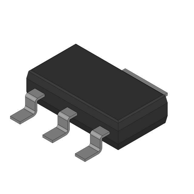
The NX1117C/NX1117CE series are housed in a medium power SOT223 (SC-73)
Surface-Mounted Device (SMD) plastic package.
Table 1.
Product overview
Output voltage Vout (V)
Output voltage accuracy
of 1 %
Output voltage accuracy
of 1.25 %
1.25 adjustable
NX1117CADJZ
NX1117CEADJZ
1.2
NX1117C12Z
NX1117CE12Z
1.5
NX1117C15Z
NX1117CE15Z
1.8
NX1117C18Z
NX1117CE18Z
1.9
NX1117C19Z
NX1117CE19Z
2.0
NX1117C20Z
NX1117CE20Z
2.5
NX1117C25Z
NX1117CE25Z
2.85
NX1117C285Z
NX1117CE285Z
3.3
NX1117C33Z
NX1117CE33Z
5.0
NX1117C50Z
NX1117CE50Z
2. Features and benefits
Maximum output current of 1 A
Wide operation range to 20 V input
Output voltage accuracy of
1 % or 1.25 %
Output current limiting
SOA control
Thermal shutdown
No minimum load requirements for fixed
output voltage versions
Temperature range 40 C to 125 C
�NX1117C; NX1117CE series
NXP Semiconductors
Low-dropout linear regulators
3. Applications
Post regulator for switching DC-to-DC converter
High-efficiency linear regulators
Battery charger
USB devices
Hard drive controllers
Consumer and industrial equipment point of load
4. Ordering information
Table 2.
Ordering information
Type number
Package
NX1117C/NX1117CE
series
Name
Description
Version
-
plastic surface-mounted package with increased
heat sink; 4 leads
SOT223
5. Marking
Table 3.
NX1117C_NX1117CE_SER
Product data sheet
Marking codes
Type number
Marking code
Type number
Marking code
NX1117CADJZ
NCADJZ
NX1117CEADJZ
7CEADJ
NX1117C12Z
N7C12Z
NX1117CE12Z
7CE12Z
NX1117C15Z
N7C15Z
NX1117CE15Z
7CE15Z
NX1117C18Z
N7C18Z
NX1117CE18Z
7CE18Z
NX1117C19Z
N7C19Z
NX1117CE19Z
7CE19Z
NX1117C20Z
N7C20Z
NX1117CE20Z
7CE20Z
NX1117C25Z
N7C25Z
NX1117CE25Z
7CE25Z
NX1117C285Z
NC285Z
NX1117CE285Z
7CE285
NX1117C33Z
N7C33Z
NX1117CE33Z
7CE33Z
NX1117C50Z
N7C50Z
NX1117CE50Z
7CE50Z
All information provided in this document is subject to legal disclaimers.
Rev. 2 — 11 December 2012
© NXP B.V. 2012. All rights reserved.
2 of 21
�NX1117C; NX1117CE series
NXP Semiconductors
Low-dropout linear regulators
6. Functional diagram
VIN
VOUT
VIN
Vref
VOUT
Vref
ADJ
OUTPUT CURRENT LIMITING
SOA CONTROL
THERMAL SHUTDOWN
OUTPUT CURRENT LIMITING
SOA CONTROL
THERMAL SHUTDOWN
GND
006aac638
Fig 1.
006aac639
Adjustable output voltage versions:
functional diagram
Fig 2.
Fixed output voltage versions:
functional diagram
7. Pinning information
Table 4.
Pinning
Pin
Symbol
Description
1
ADJ or GND
adjust or ground
2
VOUT
output
3
VIN
input
4
VOUT
output
[1]
Simplified outline
[1]
4
1
2
3
ADJ for NX1117CADJZ and NX1117CEADJZ; GND for all other devices.
8. Limiting values
Table 5.
Limiting values
In accordance with the Absolute Maximum Rating System (IEC 60134).
Symbol
Parameter
Vin
input voltage
VESD
electrostatic discharge
voltage
Conditions
MIL-STD-883
(human body model)
machine model
Ptot
total power dissipation
Product data sheet
Max
Unit
-
20
V
2
-
kV
400
-
V
internally limited
Tj
junction temperature
-
150
C
Tamb
ambient temperature
40
+125
C
Tstg
storage temperature
65
+150
C
[1]
NX1117C_NX1117CE_SER
[1]
Min
T –T
j
amb
The maximum package power dissipation is P tot = ----------------------.
R th j – a
All information provided in this document is subject to legal disclaimers.
Rev. 2 — 11 December 2012
© NXP B.V. 2012. All rights reserved.
3 of 21
�NX1117C; NX1117CE series
NXP Semiconductors
Low-dropout linear regulators
006aac644
2.5
Ptot
(W)
(1)
2.0
(2)
1.5
1.0
(3)
0.5
0.0
–75
–25
25
75
125
175
Tamb (°C)
(1) Ceramic Printed-Circuit Board (PCB), Al2O3, standard footprint
(2) FR4 PCB, mounting pad for output 6 cm2
(3) FR4 PCB, standard footprint
Fig 3.
Power derating curves
9. Recommended operating conditions
Table 6.
Recommended operation conditions
Tamb = 25 C unless otherwise specified.
Symbol
Parameter
Vin
input voltage
Conditions
Min
Max
Unit
-
20
V
10. Thermal characteristics
Table 7.
Symbol
Rth(j-a)
NX1117C_NX1117CE_SER
Product data sheet
Thermal characteristics
Parameter
thermal resistance from
junction to ambient
Conditions
in free air
Min
Typ
Max
Unit
[1]
-
-
150
K/W
[2]
-
-
72
K/W
[3]
-
-
45
K/W
Rth(j-sp)
thermal resistance from
junction to solder point
-
-
20
K/W
Tsd
shutdown temperature
-
135
-
C
[1]
Device mounted on an FR4 PCB, single-sided copper, tin-plated and standard footprint.
[2]
Device mounted on an FR4 PCB, single-sided copper, tin-plated, mounting pad for output 6 cm2.
[3]
Device mounted on a ceramic PCB, Al2O3, standard footprint.
All information provided in this document is subject to legal disclaimers.
Rev. 2 — 11 December 2012
© NXP B.V. 2012. All rights reserved.
4 of 21
�NX1117C; NX1117CE series
NXP Semiconductors
Low-dropout linear regulators
006aac645
103
Zth(j-a)
(K/W)
duty cycle = 1
102
0.75
0.33
0.5
0.2
0.1
10
0.05
0.02
0.01
1
10–1
10–5
0
10–4
10–3
10–2
10–1
1
10
102
tp (s)
103
FR4 PCB, standard footprint
Fig 4.
Transient thermal impedance from junction to ambient as a function of pulse duration; typical values
006aac646
103
Zth(j-a)
(K/W)
102
duty cycle = 1
0.75
0.33
0.5
0.2
10
0.1
0.05
0.02
1
0.01
0
10–1
10–5
10–4
10–3
10–2
10–1
1
10
102
tp (s)
103
FR4 PCB, mounting pad for output 6 cm2
Fig 5.
Transient thermal impedance from junction to ambient as a function of pulse duration; typical values
NX1117C_NX1117CE_SER
Product data sheet
All information provided in this document is subject to legal disclaimers.
Rev. 2 — 11 December 2012
© NXP B.V. 2012. All rights reserved.
5 of 21
�NX1117C; NX1117CE series
NXP Semiconductors
Low-dropout linear regulators
006aac647
102
duty cycle = 1
Zth(j-a)
(K/W)
0.75
0.5
0.33
10
0.2
0.1
0.05
0.02
1
0.01
0
10–1
10–5
10–4
10–3
10–2
10–1
1
102
10
tp (s)
103
Ceramic PCB, Al2O3, standard footprint
Fig 6.
Transient thermal impedance from junction to ambient as a function of pulse duration; typical values
11. Characteristics
Table 8.
Characteristics
Cin = 680 nF in series with 1 , and Cout = 680 nF in series with 1 . For typical value Tamb = 25 C; for minimum and
maximum values Tamb is the operating temperature range 40 C to 125 C; unless otherwise specified.
Symbol
Parameter
Vref
reference voltage
NX1117CADJZ
Conditions
Iout = 10 mA; Vin Vref = 2 V; Tamb = 25 C
10 mA Iout 800 mA; 1.5 V Vin Vref 15 V
NX1117CEADJZ
Product data sheet
All information provided in this document is subject to legal disclaimers.
Rev. 2 — 11 December 2012
Typ
Max
Unit
1.238 1.250 1.262 V
[1]
Iout = 10 mA; Vin Vref = 2 V; Tamb = 25 C
10 mA Iout 800 mA; 1.5 V Vin Vref 15 V
NX1117C_NX1117CE_SER
Min
1.225 -
1.275 V
1.234 1.250 1.266 V
[1]
1.219 -
1.281 V
© NXP B.V. 2012. All rights reserved.
6 of 21
�NX1117C; NX1117CE series
NXP Semiconductors
Low-dropout linear regulators
Table 8.
Characteristics …continued
Cin = 680 nF in series with 1 , and Cout = 680 nF in series with 1 . For typical value Tamb = 25 C; for minimum and
maximum values Tamb is the operating temperature range 40 C to 125 C; unless otherwise specified.
Symbol
Parameter
Vout
output voltage
NX1117C12Z
Conditions
Iout = 10 mA; Vin = 3.2 V; Tamb = 25 C
0 mA Iout 800 mA; 2.6 V Vin 11.2 V
NX1117CE12Z
NX1117CE15Z
NX1117C18Z
NX1117CE18Z
NX1117CE20Z
NX1117C25Z
NX1117C33Z
NX1117CE33Z
Product data sheet
All information provided in this document is subject to legal disclaimers.
Rev. 2 — 11 December 2012
1.538 V
1.836 V
1.845 V
1.881 1.900 1.919 V
1.938 V
1.876 1.900 1.924 V
[1]
1.852 -
[1]
1.960 -
1.948 V
1.980 2.000 2.020 V
2.040 V
1.975 2.000 2.025 V
[1]
1.950 -
[1]
2.450 -
2.050 V
2.475 2.500 2.525 V
2.550 V
2.469 2.500 2.531 V
[1]
2.437 -
[1]
2.790 -
2.563 V
2.820 2.850 2.880 V
2.910 V
2.814 2.850 2.886 V
[1]
2.779 -
[1]
3.235 -
2.921 V
3.267 3.300 3.333 V
3.365 V
3.259 3.300 3.341 V
[1]
3.217 -
[1]
4.900 -
3.383 V
4.950 5.000 5.050 V
Iout = 10 mA; Vin = 7.0 V; Tamb = 25 C
0 mA Iout 800 mA; 6.5 V Vin 12 V
NX1117C_NX1117CE_SER
1.862 -
Iout = 10 mA; Vin = 7.0 V; Tamb = 25 C
0 mA Iout 800 mA; 6.5 V Vin 12 V
NX1117CE50Z
[1]
Iout = 10 mA; Vin = 5.3 V; Tamb = 25 C
0 mA Iout 800 mA; 4.75 V Vin 10 V
NX1117C50Z
1.755 -
Iout = 10 mA; Vin = 5.3 V; Tamb = 25 C
0 mA Iout 800 mA; 4.75 V Vin 10 V
1.530 V
1.777 1.800 1.823 V
[1]
Iout = 10 mA; Vin = 4.85 V; Tamb = 25 C
0 mA Iout 800 mA; 4.25 V Vin 10 V
1.230 V
1.782 1.800 1.818 V
Iout = 10 mA; Vin = 4.85 V; Tamb = 25 C
0 mA Iout 800 mA; 4.25 V Vin 10 V
NX1117CE285Z
1.764 -
Iout = 10 mA; Vin = 4.5 V; Tamb = 25 C
0 mA Iout 800 mA; 3.9 V Vin 12 V
NX1117C285Z
[1]
Iout = 10 mA; Vin = 4.5 V; Tamb = 25 C
0 mA Iout 800 mA; 3.9 V Vin 12 V
NX1117CE25Z
1.462 -
Iout = 10 mA; Vin = 4.0 V; Tamb = 25 C
0 mA Iout 800 mA; 3.4 V Vin 12 V
1.224 V
1.481 1.500 1.519 V
[1]
Iout = 10 mA; Vin = 4.0 V; Tamb = 25 C
0 mA Iout 800 mA; 3.4 V Vin 12 V
Unit
1.485 1.500 1.515 V
Iout = 10 mA; Vin = 3.9 V; Tamb = 25 C
0 mA Iout 800 mA; 3.3 V Vin 11.9 V
NX1117C20Z
1.470 -
Iout = 10 mA; Vin = 3.9 V; Tamb = 25 C
0 mA Iout 800 mA; 3.3 V Vin 11.9 V
NX1117CE19Z
[1]
Iout = 10 mA; Vin = 3.8 V; Tamb = 25 C
0 mA Iout 800 mA; 3.2 V Vin 11.8 V
NX1117C19Z
1.170 -
Iout = 10 mA; Vin = 3.8 V; Tamb = 25 C
0 mA Iout 800 mA; 3.2 V Vin 11.8 V
Max
1.185 1.200 1.215 V
Iout = 10 mA; Vin = 3.5 V; Tamb = 25 C
0 mA Iout 800 mA; 2.9 V Vin 11.5 V
1.176 -
[1]
Iout = 10 mA; Vin = 3.5 V; Tamb = 25 C
0 mA Iout 800 mA; 2.9 V Vin 11.5 V
Typ
1.188 1.200 1.212 V
[1]
Iout = 10 mA; Vin = 3.2 V; Tamb = 25 C
0 mA Iout 800 mA; 2.6 V Vin 11.2 V
NX1117C15Z
Min
5.100 V
4.937 5.000 5.063 V
[1]
4.875 -
5.125 V
© NXP B.V. 2012. All rights reserved.
7 of 21
�NX1117C; NX1117CE series
NXP Semiconductors
Low-dropout linear regulators
Table 8.
Characteristics …continued
Cin = 680 nF in series with 1 , and Cout = 680 nF in series with 1 . For typical value Tamb = 25 C; for minimum and
maximum values Tamb is the operating temperature range 40 C to 125 C; unless otherwise specified.
Symbol
Parameter
Conditions
Vdo
dropout voltage
measured at Vout 100 mV
Max
Unit
Iout = 100 mA
-
0.95
1.1
V
-
1.01
1.15
V
Iout = 800 mA
-
1.07
1.2
V
Vin Vout = 5.0 V; Tamb = 25 C
1000
1200
1500
mA
NX1117C12Z;
NX1117CE12Z
Vin = 11.2 V
-
5
6
mA
NX1117C15Z;
NX1117CE15Z
Vin = 11.5 V
-
5
6
mA
NX1117C18Z;
NX1117CE18Z
Vin = 11.8 V
-
5
6
mA
NX1117C19Z;
NX1117CE19Z
Vin = 11.9 V
-
5
6
mA
NX1117C20Z;
NX1117CE20Z
Vin = 12 V
-
5
6
mA
NX1117C25Z;
NX1117CE25Z
Vin = 10 V
-
5
6
mA
NX1117C285Z;
NX1117CE285Z
Vin = 10 V
-
5
6
mA
NX1117C33Z;
NX1117CE33Z
Vin = 15 V
-
5
6
mA
NX1117C50Z;
NX1117CE50Z
Vin = 15 V
-
5
6
mA
Vin = 11.25 V; Iout = 800 mA
-
52
120
A
1.4 V Vin Vout 10 V; 10 mA Iout 800 mA
-
0.4
5
A
output current limit
Iq
quiescent current
adjust current
NX1117CADJZ;
NX1117CEADJZ
Iadj
Typ
Iout = 500 mA
Iout(lim)
Iadj
Min
adjust current variation
NX1117CADJZ;
NX1117CEADJZ
NX1117C_NX1117CE_SER
Product data sheet
All information provided in this document is subject to legal disclaimers.
Rev. 2 — 11 December 2012
© NXP B.V. 2012. All rights reserved.
8 of 21
�NX1117C; NX1117CE series
NXP Semiconductors
Low-dropout linear regulators
Table 8.
Characteristics …continued
Cin = 680 nF in series with 1 , and Cout = 680 nF in series with 1 . For typical value Tamb = 25 C; for minimum and
maximum values Tamb is the operating temperature range 40 C to 125 C; unless otherwise specified.
Symbol
Parameter
Conditions
Min
Typ
Max
Unit
-
0.8
5
mA
NX1117CADJZ;
NX1117CEADJZ
-
69
-
dB
NX1117C12Z;
NX1117CE12Z
-
72
-
dB
NX1117C15Z;
NX1117CE15Z
-
69
-
dB
NX1117C18Z;
NX1117CE18Z
-
68
-
dB
NX1117C19Z;
NX1117CE19Z
-
67
-
dB
NX1117C20Z;
NX1117CE20Z
-
67
-
dB
NX1117C25Z;
NX1117CE25Z
-
65
-
dB
NX1117C285Z;
NX1117CE285Z
-
63
-
dB
NX1117C33Z;
NX1117CE33Z
-
62
-
dB
NX1117C50Z;
NX1117CE50Z
-
59
-
dB
-
0.003 -
Regulation characteristics
Iout(min)
minimum output current
NX1117CADJZ;
NX1117CEADJZ
PSRR
required for regulation
Vin = 15 V
power supply ripple rejection Vin Vout = 2.4 V; Iout = 40 mA;
2 V(p-p) 120 Hz sine wave
Vn(out)RMS RMS output noise voltage
NX1117C_NX1117CE_SER
Product data sheet
10 Hz f 10 kHz
All information provided in this document is subject to legal disclaimers.
Rev. 2 — 11 December 2012
%
© NXP B.V. 2012. All rights reserved.
9 of 21
�NX1117C; NX1117CE series
NXP Semiconductors
Low-dropout linear regulators
Table 8.
Characteristics …continued
Cin = 680 nF in series with 1 , and Cout = 680 nF in series with 1 . For typical value Tamb = 25 C; for minimum and
maximum values Tamb is the operating temperature range 40 C to 125 C; unless otherwise specified.
Symbol
Parameter
Conditions
Min
Typ
Max
Unit
Line regulation
Vout
[2]
output voltage variation
NX1117CADJZ;
NX1117CEADJZ
Iout = 10 mA; 2.75 V Vin 16.25 V
-
0.1
0.3
%
NX1117C12Z;
NX1117CE12Z
Iout = 0 mA; 2.6 V Vin 11.2 V
-
1.2
3.0
mV
NX1117C15Z;
NX1117CE15Z
Iout = 0 mA; 2.9 V Vin 11.5 V
-
1.5
3.5
mV
NX1117C18Z;
NX1117CE18Z
Iout = 0 mA; 3.2 V Vin 11.8 V
-
1.8
4.0
mV
NX1117C19Z;
NX1117CE19Z
Iout = 0 mA; 3.3 V Vin 11.9 V
-
1.9
4.0
mV
NX1117C20Z;
NX1117CE20Z
Iout = 0 mA; 3.4 V Vin 12 V
-
2.0
4.5
mV
NX1117C25Z;
NX1117CE25Z
Iout = 0 mA; 3.9 V Vin 12 V
-
2.5
4.5
mV
NX1117C285Z;
NX1117CE285Z
Iout = 0 mA; 4.25 V Vin 10 V
-
2.5
4.5
mV
NX1117C33Z;
NX1117CE33Z
Iout = 0 mA; 4.75 V Vin 10 V
-
2.5
4.5
mV
NX1117C50Z;
NX1117CE50Z
Iout = 0 mA; 6.5 V Vin 12 V
-
6.0
10
mV
Load regulation
Vout
[2]
output voltage variation
NX1117CADJZ;
NX1117CEADJZ
Vin Vout = 1.4 V; 10 mA Iout 800 mA
-
0.2
0.4
%
NX1117C12Z;
NX1117CE12Z
Vin = 2.6 V; 0 mA Iout 800 mA
-
1
4
mV
NX1117C15Z;
NX1117CE15Z
Vin = 2.9 V; 0 mA Iout 800 mA
-
1
5
mV
NX1117C18Z;
NX1117CE18Z
Vin = 3.2 V; 0 mA Iout 800 mA
-
1
5
mV
NX1117C19Z;
NX1117CE19Z
Vin = 3.3 V; 0 mA Iout 800 mA
-
1
6
mV
NX1117C20Z;
NX1117CE20Z
Vin = 3.4 V; 0 mA Iout 800 mA
-
1
6
mV
NX1117C25Z;
NX1117CE25Z
Vin = 3.9 V; 0 mA Iout 800 mA
-
1
6
mV
NX1117C285Z;
NX1117CE285Z
Vin = 4.25 V; 0 mA Iout 800 mA
-
1
7
mV
NX1117C33Z;
NX1117CE33Z
Vin = 4.75 V; 0 mA Iout 800 mA
-
1
7
mV
NX1117C50Z;
NX1117CE50Z
Vin = 6.5 V; 0 mA Iout 800 mA
-
1
10
mV
NX1117C_NX1117CE_SER
Product data sheet
All information provided in this document is subject to legal disclaimers.
Rev. 2 — 11 December 2012
© NXP B.V. 2012. All rights reserved.
10 of 21
�NX1117C; NX1117CE series
NXP Semiconductors
Low-dropout linear regulators
Table 8.
Characteristics …continued
Cin = 680 nF in series with 1 , and Cout = 680 nF in series with 1 . For typical value Tamb = 25 C; for minimum and
maximum values Tamb is the operating temperature range 40 C to 125 C; unless otherwise specified.
Symbol
Parameter
Conditions
Min
Typ
Max
Unit
40 C Tamb 125 C
-
0.7
-
%
1000 h end-point measurement; Tamb = 25 C
-
0.3
-
%
Temperature stability
Vout
output voltage variation
Long-term stability
Vout
output voltage variation
[1]
The SOA control limits the output current at high voltage differences Vin Vout in order to keep the device in the safe operating area.
[2]
During testing low duty cycle pulse techniques are used to maintain the junction temperature as close to ambient as possible.
006aac659
2
∆Vout
(%)
006aac660
1.4
Vdo
(V)
1.2
1
(1)
(2)
1.0
(3)
0.8
0
0.6
0.4
–1
0.2
–2
–50
0
50
0.0
100
150
Tamb (°C)
0
200
400
600
Iout (mA)
800
Load pulsed at 1 % duty cycle
Vin = Vout + 2 V
(1) Tamb = 40 C
Iout = 10 mA
(2) Tamb = 25 C
(3) Tamb = 125 C
Fig 7.
Output voltage variation as a function of
ambient temperature; typical values
NX1117C_NX1117CE_SER
Product data sheet
Fig 8.
Dropout voltage as a function of output
current; typical values
All information provided in this document is subject to legal disclaimers.
Rev. 2 — 11 December 2012
© NXP B.V. 2012. All rights reserved.
11 of 21
�NX1117C; NX1117CE series
NXP Semiconductors
Low-dropout linear regulators
006aac661
1.5
006aac662
1.5
Iout(lim)
(A)
Iout(lim)
(A)
1.3
1.0
1.1
0.5
0.9
0.0
Fig 9.
0
4
8
12
16
20
Vin – Vout (V)
0.7
–50
0
50
Tamb = 25 C
Vin = 5 V
Load pulsed at 1 % duty cycle
Load pulsed at 1 % duty cycle
Output current limit as a function of voltage
difference Vin Vout
006aac663
100
Iadj
(μA)
100
150
Tamb (°C)
Fig 10. Output current limit as a function of ambient
temperature
006aac664
10
∆Iq
(%)
80
0
60
40
–10
20
0
–50
0
50
100
150
Tamb (°C)
–20
–50
0
50
100
150
Tamb (°C)
Vin = 3.25 V
Iout = 10 mA
Fig 11. Adjustable output voltage versions:
Adjust current as a function of ambient
temperature; typical values
NX1117C_NX1117CE_SER
Product data sheet
Fig 12. Fixed output voltage versions:
Quiescent current variation as a function of
ambient temperature; typical values
All information provided in this document is subject to legal disclaimers.
Rev. 2 — 11 December 2012
© NXP B.V. 2012. All rights reserved.
12 of 21
�NX1117C; NX1117CE series
NXP Semiconductors
Low-dropout linear regulators
006aac665
100
PSRR
(dB)
PSRR
(dB)
80
80
60
60
40
40
20
20
0
006aac666
100
0
200
400
600
800
1000
Iout (mA)
0
10
102
Vout = 1.25 V;
Vin Vout = 2.4 V;
Vin Vout = 2.4 V;
Iout = 40 mA;
Cout = 680 nF;
Cout = 10 F;
Tamb = 25 C;
Tamb = 25 C;
2 V(p-p); 120 Hz sine wave
Product data sheet
104
f (Hz)
105
2 V(p-p)
Fig 13. Adjustable output voltage versions:
Power supply ripple rejection as a function of
output current; typical values
NX1117C_NX1117CE_SER
103
Fig 14. Power supply ripple rejection as a function of
frequency; typical values
All information provided in this document is subject to legal disclaimers.
Rev. 2 — 11 December 2012
© NXP B.V. 2012. All rights reserved.
13 of 21
�NX1117C; NX1117CE series
NXP Semiconductors
Low-dropout linear regulators
006aac667
6.25
006aac668
8.5
Vin
(V)
Vin
(V)
4.25
6.5
20
20
∆Vout
(mV)
∆Vout
(mV)
–20
–20
0
40
80
120
160
t (μs)
200
0
40
Cout = 10 F;
Cout = 10 F;
Iout = 100 mA;
Iout = 100 mA;
Tamb = 25 C
Tamb = 25 C
Fig 15. NX1117C285Z and NX1117CE285Z:
Line transient response as a function of time;
typical values
80
120
160
t (μs)
200
Fig 16. NX1117C50Z and NX1117CE50Z:
Line transient response as a function of time;
typical values
006aac669
006aac670
0.1
0.1
∆Vout
(V)
∆Vout
(V)
–0.1
–0.1
1
1
Iout
(A)
Iout
(A)
0
0
0
40
80
120
160
t (μs)
200
Cin = 10 F;
0
40
80
Cout = 10 F;
Vin = 4.5 V
Vin = 6.5 V
Tamb = 25 C;
Tamb = 25 C;
Preload = 100 mA
Preload = 100 mA
Fig 17. NX1117C285Z and NX1117CE285Z:
Load transient response as a function of time;
typical values
Product data sheet
160
t (μs)
200
Cin = 10 F;
Cout = 10 F;
NX1117C_NX1117CE_SER
120
Fig 18. NX1117C50Z and NX1117CE50Z:
Load transient response as a function of time;
typical values
All information provided in this document is subject to legal disclaimers.
Rev. 2 — 11 December 2012
© NXP B.V. 2012. All rights reserved.
14 of 21
�NX1117C; NX1117CE series
NXP Semiconductors
Low-dropout linear regulators
12. Application information
approx. 5 V
VIN
VOUT
NX1117C33Z
NX1117CE33Z
10 μF
3.3 V
10 μF
006aac640
Fig 19. NX1117C33Z and NX1117CE33Z: Typical application for fixed output voltage
versions
NX1117CADJZ
NX1117CEADJZ
VIN
VOUT
R1
10 μF
10 μF
R2
006aac641
V OUT = V ref 1 + R2 R1 + I adj R2
Fig 20. NX1117CADJZ and NX1117CEADJZ: Typical application for adjustable output
voltage versions
NX1117C_NX1117CE_SER
Product data sheet
All information provided in this document is subject to legal disclaimers.
Rev. 2 — 11 December 2012
© NXP B.V. 2012. All rights reserved.
15 of 21
�NX1117C; NX1117CE series
NXP Semiconductors
Low-dropout linear regulators
13. Package outline
6.7
6.3
3.1
2.9
1.8
1.5
4
1.1
0.7
7.3
6.7
3.7
3.3
1
2
3
2.3
4.6
0.8
0.6
0.32
0.22
Dimensions in mm
04-11-10
Fig 21. Package outline SOT223 (SC-73)
14. Packing information
Table 9.
Packing methods
The indicated -xxx are the last three digits of the 12NC ordering code.[1]
Type number
Package
NX1117C/NX1117CE
series
[1]
NX1117C_NX1117CE_SER
Product data sheet
SOT223
Description
8 mm pitch, 12 mm tape and reel
Packing quantity
1000
4000
-115
-135
For further information and the availability of packing methods, see Section 18.
All information provided in this document is subject to legal disclaimers.
Rev. 2 — 11 December 2012
© NXP B.V. 2012. All rights reserved.
16 of 21
�NX1117C; NX1117CE series
NXP Semiconductors
Low-dropout linear regulators
15. Soldering
7
3.85
3.6
3.5
0.3
1.3 1.2
(4×) (4×)
solder lands
4
solder resist
3.9
6.1 7.65
solder paste
occupied area
1
2
3
Dimensions in mm
2.3
2.3
1.2
(3×)
1.3
(3×)
6.15
sot223_fr
Fig 22. Reflow soldering footprint SOT223 (SC-73)
8.9
6.7
1.9
solder lands
4
solder resist
6.2
8.7
occupied area
Dimensions in mm
1
2
3
1.9
(3×)
2.7
preferred transport
direction during soldering
2.7
1.1
1.9
(2×)
sot223_fw
Fig 23. Wave soldering footprint SOT223 (SC-73)
NX1117C_NX1117CE_SER
Product data sheet
All information provided in this document is subject to legal disclaimers.
Rev. 2 — 11 December 2012
© NXP B.V. 2012. All rights reserved.
17 of 21
�NX1117C; NX1117CE series
NXP Semiconductors
Low-dropout linear regulators
16. Revision history
Table 10.
Revision history
Document ID
Release date
NX1117C_NX1117CE_SER v.2 20121211
Modifications:
•
•
Product data sheet
Change notice Supersedes
Product data sheet
-
NX1117C_NX1117CE_SER v.1
Table 7 “Thermal characteristics”: added shutdown temperature Tsd
Electrostatic discharge voltage VESD moved from Table 8 to Table 5
NX1117C_NX1117CE_SER v.1 20110718
NX1117C_NX1117CE_SER
Data sheet status
Product data sheet
-
All information provided in this document is subject to legal disclaimers.
Rev. 2 — 11 December 2012
-
© NXP B.V. 2012. All rights reserved.
18 of 21
�NX1117C; NX1117CE series
NXP Semiconductors
Low-dropout linear regulators
17. Legal information
17.1 Data sheet status
Document status[1][2]
Product status[3]
Definition
Objective [short] data sheet
Development
This document contains data from the objective specification for product development.
Preliminary [short] data sheet
Qualification
This document contains data from the preliminary specification.
Product [short] data sheet
Production
This document contains the product specification.
[1]
Please consult the most recently issued document before initiating or completing a design.
[2]
The term ‘short data sheet’ is explained in section “Definitions”.
[3]
The product status of device(s) described in this document may have changed since this document was published and may differ in case of multiple devices. The latest product status
information is available on the Internet at URL http://www.nxp.com.
17.2 Definitions
Draft — The document is a draft version only. The content is still under
internal review and subject to formal approval, which may result in
modifications or additions. NXP Semiconductors does not give any
representations or warranties as to the accuracy or completeness of
information included herein and shall have no liability for the consequences of
use of such information.
Short data sheet — A short data sheet is an extract from a full data sheet
with the same product type number(s) and title. A short data sheet is intended
for quick reference only and should not be relied upon to contain detailed and
full information. For detailed and full information see the relevant full data
sheet, which is available on request via the local NXP Semiconductors sales
office. In case of any inconsistency or conflict with the short data sheet, the
full data sheet shall prevail.
Product specification — The information and data provided in a Product
data sheet shall define the specification of the product as agreed between
NXP Semiconductors and its customer, unless NXP Semiconductors and
customer have explicitly agreed otherwise in writing. In no event however,
shall an agreement be valid in which the NXP Semiconductors product is
deemed to offer functions and qualities beyond those described in the
Product data sheet.
17.3 Disclaimers
Limited warranty and liability — Information in this document is believed to
be accurate and reliable. However, NXP Semiconductors does not give any
representations or warranties, expressed or implied, as to the accuracy or
completeness of such information and shall have no liability for the
consequences of use of such information. NXP Semiconductors takes no
responsibility for the content in this document if provided by an information
source outside of NXP Semiconductors.
In no event shall NXP Semiconductors be liable for any indirect, incidental,
punitive, special or consequential damages (including - without limitation - lost
profits, lost savings, business interruption, costs related to the removal or
replacement of any products or rework charges) whether or not such
damages are based on tort (including negligence), warranty, breach of
contract or any other legal theory.
Notwithstanding any damages that customer might incur for any reason
whatsoever, NXP Semiconductors’ aggregate and cumulative liability towards
customer for the products described herein shall be limited in accordance
with the Terms and conditions of commercial sale of NXP Semiconductors.
Right to make changes — NXP Semiconductors reserves the right to make
changes to information published in this document, including without
limitation specifications and product descriptions, at any time and without
notice. This document supersedes and replaces all information supplied prior
to the publication hereof.
NX1117C_NX1117CE_SER
Product data sheet
Suitability for use — NXP Semiconductors products are not designed,
authorized or warranted to be suitable for use in life support, life-critical or
safety-critical systems or equipment, nor in applications where failure or
malfunction of an NXP Semiconductors product can reasonably be expected
to result in personal injury, death or severe property or environmental
damage. NXP Semiconductors and its suppliers accept no liability for
inclusion and/or use of NXP Semiconductors products in such equipment or
applications and therefore such inclusion and/or use is at the customer’s own
risk.
Applications — Applications that are described herein for any of these
products are for illustrative purposes only. NXP Semiconductors makes no
representation or warranty that such applications will be suitable for the
specified use without further testing or modification.
Customers are responsible for the design and operation of their applications
and products using NXP Semiconductors products, and NXP Semiconductors
accepts no liability for any assistance with applications or customer product
design. It is customer’s sole responsibility to determine whether the NXP
Semiconductors product is suitable and fit for the customer’s applications and
products planned, as well as for the planned application and use of
customer’s third party customer(s). Customers should provide appropriate
design and operating safeguards to minimize the risks associated with their
applications and products.
NXP Semiconductors does not accept any liability related to any default,
damage, costs or problem which is based on any weakness or default in the
customer’s applications or products, or the application or use by customer’s
third party customer(s). Customer is responsible for doing all necessary
testing for the customer’s applications and products using NXP
Semiconductors products in order to avoid a default of the applications and
the products or of the application or use by customer’s third party
customer(s). NXP does not accept any liability in this respect.
Limiting values — Stress above one or more limiting values (as defined in
the Absolute Maximum Ratings System of IEC 60134) will cause permanent
damage to the device. Limiting values are stress ratings only and (proper)
operation of the device at these or any other conditions above those given in
the Recommended operating conditions section (if present) or the
Characteristics sections of this document is not warranted. Constant or
repeated exposure to limiting values will permanently and irreversibly affect
the quality and reliability of the device.
Terms and conditions of commercial sale — NXP Semiconductors
products are sold subject to the general terms and conditions of commercial
sale, as published at http://www.nxp.com/profile/terms, unless otherwise
agreed in a valid written individual agreement. In case an individual
agreement is concluded only the terms and conditions of the respective
agreement shall apply. NXP Semiconductors hereby expressly objects to
applying the customer’s general terms and conditions with regard to the
purchase of NXP Semiconductors products by customer.
No offer to sell or license — Nothing in this document may be interpreted or
construed as an offer to sell products that is open for acceptance or the grant,
conveyance or implication of any license under any copyrights, patents or
other industrial or intellectual property rights.
All information provided in this document is subject to legal disclaimers.
Rev. 2 — 11 December 2012
© NXP B.V. 2012. All rights reserved.
19 of 21
�NX1117C; NX1117CE series
NXP Semiconductors
Low-dropout linear regulators
Export control — This document as well as the item(s) described herein
may be subject to export control regulations. Export might require a prior
authorization from competent authorities.
Quick reference data — The Quick reference data is an extract of the
product data given in the Limiting values and Characteristics sections of this
document, and as such is not complete, exhaustive or legally binding.
Non-automotive qualified products — Unless this data sheet expressly
states that this specific NXP Semiconductors product is automotive qualified,
the product is not suitable for automotive use. It is neither qualified nor tested
in accordance with automotive testing or application requirements. NXP
Semiconductors accepts no liability for inclusion and/or use of
non-automotive qualified products in automotive equipment or applications.
In the event that customer uses the product for design-in and use in
automotive applications to automotive specifications and standards, customer
(a) shall use the product without NXP Semiconductors’ warranty of the
product for such automotive applications, use and specifications, and (b)
whenever customer uses the product for automotive applications beyond
NXP Semiconductors’ specifications such use shall be solely at customer’s
own risk, and (c) customer fully indemnifies NXP Semiconductors for any
liability, damages or failed product claims resulting from customer design and
use of the product for automotive applications beyond NXP Semiconductors’
standard warranty and NXP Semiconductors’ product specifications.
17.4 Trademarks
Notice: All referenced brands, product names, service names and trademarks
are the property of their respective owners.
18. Contact information
For more information, please visit: http://www.nxp.com
For sales office addresses, please send an email to: salesaddresses@nxp.com
NX1117C_NX1117CE_SER
Product data sheet
All information provided in this document is subject to legal disclaimers.
Rev. 2 — 11 December 2012
© NXP B.V. 2012. All rights reserved.
20 of 21
�NXP Semiconductors
NX1117C; NX1117CE series
Low-dropout linear regulators
19. Contents
1
2
3
4
5
6
7
8
9
10
11
12
13
14
15
16
17
17.1
17.2
17.3
17.4
18
19
General description . . . . . . . . . . . . . . . . . . . . . . 1
Features and benefits . . . . . . . . . . . . . . . . . . . . 1
Applications . . . . . . . . . . . . . . . . . . . . . . . . . . . . 2
Ordering information . . . . . . . . . . . . . . . . . . . . . 2
Marking . . . . . . . . . . . . . . . . . . . . . . . . . . . . . . . . 2
Functional diagram . . . . . . . . . . . . . . . . . . . . . . 3
Pinning information . . . . . . . . . . . . . . . . . . . . . . 3
Limiting values. . . . . . . . . . . . . . . . . . . . . . . . . . 3
Recommended operating conditions. . . . . . . . 4
Thermal characteristics . . . . . . . . . . . . . . . . . . 4
Characteristics . . . . . . . . . . . . . . . . . . . . . . . . . . 6
Application information. . . . . . . . . . . . . . . . . . 15
Package outline . . . . . . . . . . . . . . . . . . . . . . . . 16
Packing information . . . . . . . . . . . . . . . . . . . . 16
Soldering . . . . . . . . . . . . . . . . . . . . . . . . . . . . . 17
Revision history . . . . . . . . . . . . . . . . . . . . . . . . 18
Legal information. . . . . . . . . . . . . . . . . . . . . . . 19
Data sheet status . . . . . . . . . . . . . . . . . . . . . . 19
Definitions . . . . . . . . . . . . . . . . . . . . . . . . . . . . 19
Disclaimers . . . . . . . . . . . . . . . . . . . . . . . . . . . 19
Trademarks. . . . . . . . . . . . . . . . . . . . . . . . . . . 20
Contact information. . . . . . . . . . . . . . . . . . . . . 20
Contents . . . . . . . . . . . . . . . . . . . . . . . . . . . . . . 21
Please be aware that important notices concerning this document and the product(s)
described herein, have been included in section ‘Legal information’.
© NXP B.V. 2012.
All rights reserved.
For more information, please visit: http://www.nxp.com
For sales office addresses, please send an email to: salesaddresses@nxp.com
Date of release: 11 December 2012
Document identifier: NX1117C_NX1117CE_SER
�


 工商网监
湘ICP备2023018690号
工商网监
湘ICP备2023018690号
