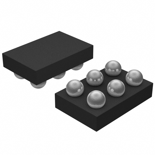
NX5P2925C
Logic controlled high-side power switch
Rev. 1 — 7 July 2015
Product data sheet
1. General description
The NX5P2925C is a high-side load switch which features a low ON resistance N-channel
MOSFET with controlled slew rate that supports 2.5 A of continuous current. Designed for
operation from 0.8 V to 5.5 V, it is used in power domain isolation applications to reduce
power dissipation and extend battery life. The enable logic includes integrated logic level
translation making the device compatible with lower voltage processors and controllers.
The NX5P2925C is ideal for portable, battery operated applications due to low ground
current.
NX5P2925C features reverse current protection (RCP) circuits. If VOUT exceeds VIN by
25 mV, the RCP circuit isolates VOUT from VIN, preventing damage to devices on the
input side of the switch.
2. Features and benefits
Wide supply voltage range from 0.8 V to 5.5 V
Very low ON resistance:
18 m (typical) at a supply voltage of 1.2 V
18 m (typical) at a supply voltage of 1.8 V
High noise immunity
High current handling capability (2.5 A continuous current)
Reverse current protection
Turn-on slew rate limiting
ESD protection:
HBM JESD22-A114F Class 3A exceeds 5000 V
CDM AEC-Q100-011 revision B exceeds 1000 V
Specified from 40 C to +85 C
3. Applications
Cell phone
Digital cameras and audio devices
Portable and battery-powered equipment
�NX5P2925C
NXP Semiconductors
Logic controlled high-side power switch
4. Ordering information
Table 1.
Ordering information
Type number
NX5P2925CUK
Package
Temperature range
Name
Description
Version
40 C to +85 C
WLCSP6
wafer level chip-scale package; 6 bumps;
0.87 1.37 0.5 mm
NX5P2925C
5. Marking
Table 2.
Marking codes
Type number
Marking code
NX5P2925CUK
5C
6. Functional diagram
EN
VIN
VOUT
001aao342
Fig 1.
Logic symbol
5(9(56(�&855(17
3527(&7,21
9,1
(1
9287
&+$5*(�3803�
6/(:�5$7(�&21752/
$1'�/2$'�',6&+$5*(
DDD�������
Fig 2.
Logic diagram
NX5P2925C
Product data sheet
All information provided in this document is subject to legal disclaimers.
Rev. 1 — 7 July 2015
© NXP Semiconductors N.V. 2015. All rights reserved.
2 of 20
�NX5P2925C
NXP Semiconductors
Logic controlled high-side power switch
7. Pinning information
7.1 Pinning
EXPS�$�
LQGH[�DUHD
�
�
$
%
&
7UDQVSDUHQW�WRS�YLHZ
�
�
$
9287
9,1
%
9287
9,1
&
*1'
(1
7UDQVSDUHQW�WRS�YLHZ
DDD�������
DDD�������
Fig 3.
Pin configuration for WLCSP6
Fig 4.
Ball mapping for WLCSP6
7.2 Pin description
Table 3.
Pin description
Symbol
Pin
Description
VIN
A2, B2
input voltage
GND
C1
ground (0 V)
EN
C2
enable input (active HIGH)
VOUT
A1, B1
output voltage
8. Functional description
Table 4.
Function table[1]
Input EN
Switch
L
switch OFF
H
switch ON
[1]
H = HIGH voltage level; L = LOW voltage level.
NX5P2925C
Product data sheet
All information provided in this document is subject to legal disclaimers.
Rev. 1 — 7 July 2015
© NXP Semiconductors N.V. 2015. All rights reserved.
3 of 20
�NX5P2925C
NXP Semiconductors
Logic controlled high-side power switch
9. Application diagram
The NX5P2925C is typically used in portable, battery operated device. Pin EN enables
the NX5P2925C. Slew rate controlled in-rush current reduction circuits function during
switching.
9287
9,1
(1
&,1
����)
1;�3����&
&287
����)
(1
*1'
DDD�������
Fig 5.
NX5P2925C application diagram
NX5P2925C
Product data sheet
All information provided in this document is subject to legal disclaimers.
Rev. 1 — 7 July 2015
© NXP Semiconductors N.V. 2015. All rights reserved.
4 of 20
�NX5P2925C
NXP Semiconductors
Logic controlled high-side power switch
10. Limiting values
Table 5.
Limiting values
In accordance with the Absolute Maximum Rating System (IEC 60134). Voltages are referenced to GND (ground = 0 V).
Symbol
Parameter
input voltage
VI
Conditions
Min
Max
Unit
input EN
[1]
0.5
VI(VIN)
V
0.5
+6.0
V
0.5
VI(VIN)
V
input VIN
[2]
VSW
switch voltage
output VOUT
[2]
IIK
input clamping current
input EN: VI(EN) < 0.5 V
50
-
mA
ISK
switch clamping current
input VIN: VI(VIN) < 0.5 V
50
-
mA
switch current
ISW
Tj(max)
maximum junction
temperature
Tstg
storage temperature
output VOUT: VO(VOUT) < 0.5 V
50
-
mA
output VOUT: VO(VOUT) > VI(VIN) 0.5 V
-
50
mA
VSW > 0.5 V
-
2500
mA
pulsed, 100 ms pulse, 2 % duty cycle
-
5000
mA
40
+125
C
65
+150
C
-
470
mW
[3]
total power dissipation
Ptot
[1]
The minimum input voltage rating may be exceeded if the input current rating is observed.
[2]
The minimum and maximum switch voltage ratings may be exceeded if the switch clamping current rating is observed.
[3]
The (absolute) maximum power dissipation depends on the junction temperature Tj. Higher power dissipation is allowed in conjunction
with lower ambient temperatures. The conditions to determine the specified values are Tamb = 85 °C and the use of a two layer PCB.
11. Recommended operating conditions
Table 6.
Recommended operating conditions
Symbol Parameter
VI
Tamb
input voltage
Conditions
Min
Max
Unit
input EN
0
VI(VIN)
V
input VIN
0.8
5.5
V
40
+85
C
ambient temperature
NX5P2925C
Product data sheet
All information provided in this document is subject to legal disclaimers.
Rev. 1 — 7 July 2015
© NXP Semiconductors N.V. 2015. All rights reserved.
5 of 20
�NX5P2925C
NXP Semiconductors
Logic controlled high-side power switch
12. Thermal characteristics
Table 7.
Symbol
Rth(j-a)
[1]
Thermal characteristics
Parameter
Conditions
[1]
thermal resistance from junction to ambient
Typ
Unit
139
K/W
Rth(j-a) is dependent upon board layout. To minimize Rth(j-a), ensure that all pins have a solid connection to larger copper layer areas. In
multi-layer PCBs, the second layer should be used to create a large heat spreader area below the device. Avoid using solder-stop
varnish under the device.
13. Static characteristics
Table 8.
Static characteristics
VI(VIN) = 1.0 V to 5.5 V, unless otherwise specified; Voltages are referenced to GND (ground = 0 V).
Symbol Parameter
VIH
VIL
HIGH-level input
voltage
LOW-level input
voltage
Tamb = 25 C
Conditions
Tamb = 40 C to +85 C
Unit
Min
Typ[1]
Max
Min
Max
EN input; VI(VIN) = 0.8 V
0.6
-
-
0.6
-
V
EN input; VI(VIN) = 1.0 V to 1.2 V
0.9
-
-
0.9
-
V
EN input; VI(VIN) = 1.2 V to 2.5 V
1.2
-
-
1.2
-
V
EN input; VI(VIN) = 2.5 V to 5.5 V
1.2
-
-
1.2
-
V
EN input; VI(VIN) = 0.8 V
-
-
0.25
-
0.25
V
EN input; VI(VIN) = 1.0 V to 1.2 V
-
-
0.3
-
0.3
V
EN input; VI(VIN) = 1.2 V to 2.5 V
-
-
0.4
-
0.4
EN input; VI(VIN) = 2.5 V to 5.5 V
-
-
0.6
-
0.6
II
input leakage
current
EN input; VI(EN) = 0.9 V to 5.5 V
-
-
-
-
0.1
A
Vtrig
trigger voltage
RCP; Vtrig = V(VOUT) V(VIN)
-
25
-
-
40
mV
VH
hysteresis
voltage
Vtrig
-
3
-
-
15
mV
IDD
supply current
VOUT open
EN = HIGH; VI(VIN) = 1.0 V;
see Figure 6 and Figure 7
-
45
-
-
65
A
EN = HIGH; VI(VIN) = 1.8 V;
see Figure 6 and Figure 7
-
50
-
-
70
A
EN = HIGH; VI(VIN) = 3.6 V;
see Figure 6 and Figure 7
-
65
-
-
95
A
EN = HIGH; VI(VIN) = 5.5 V;
see Figure 6 and Figure 7
-
115
-
-
150
A
EN = LOW;
-
0.1
-
-
1.5
A
see Figure 8 and Figure 9
NX5P2925C
Product data sheet
All information provided in this document is subject to legal disclaimers.
Rev. 1 — 7 July 2015
© NXP Semiconductors N.V. 2015. All rights reserved.
6 of 20
�NX5P2925C
NXP Semiconductors
Logic controlled high-side power switch
Table 8.
Static characteristics …continued
VI(VIN) = 1.0 V to 5.5 V, unless otherwise specified; Voltages are referenced to GND (ground = 0 V). …continued
Symbol Parameter
IS(OFF)
Tamb = 25 C
Conditions
OFF-state
leakage current
Tamb = 40 C to +85 C
Unit
Min
Typ[1]
Max
Min
Max
EN = LOW; VI(VIN) = 1.8 V;
VI(VOUT) = 0 V; see Figure 10 and
Figure 11
-
0.5
-
3.5
-
A
EN = LOW; VI(VIN) = 3.6 V;
VI(VOUT) = 0 V; see Figure 10 and
Figure 11
-
0.5
-
5.0
-
A
EN = LOW; VI(VIN) = 5.5 V;
VI(VOUT) = 0 V; see Figure 10 and
Figure 11
-
0.5
-
7.5
-
A
CI
input capacitance EN
-
3
-
-
-
pF
CS(ON)
ON-state
capacitance
-
-
0.5
-
0.5
nF
[1]
VIN; VOUT
All typical values are measured at VI(VIN) = 3.6 V and Tamb = 25 C unless otherwise specified.
13.1 Graphs
DDD�������
���
,�9,1�
�X$�
���
���
��
��
���
���
���
���
��
��
��
��
��
���
DDD�������
���
,�9,1�
�X$�
���
��
��
��
7DPE��&�
��
��
���
���
���
�
���
���
���
���
9,�9,1���9�
���
VI(EN) = VI(VIN).
VI(EN) = VI(VIN).
(1) VI(VIN) = 5.5 V.
(1) Tamb = +85 C.
(2) VI(VIN) = 3.6 V.
(2) Tamb = +25 C.
(3) VI(VIN) = 1.8 V.
(3) Tamb = 40 C.
(4) VI(VIN) = 1.0 V.
Fig 6.
Typical supply current versus temperature
NX5P2925C
Product data sheet
Fig 7.
Typical supply current versus input voltage on
pin VIN
All information provided in this document is subject to legal disclaimers.
Rev. 1 — 7 July 2015
© NXP Semiconductors N.V. 2015. All rights reserved.
7 of 20
�NX5P2925C
NXP Semiconductors
Logic controlled high-side power switch
DDD�������
��
DDD�������
���
O�9,1�
�Q$�
O�9,1�
�Q$�
��
���
��
��
���
��
��
���
���
��
��
���
���
���
���
�
���
�
���
��
��
��
7DPE��&�
��
�
VI(EN) = GND.
���
���
���
���
9,�9,1���9�
���
VI(EN) = GND.
(1) VI(VIN) = 5.5 V.
(1) Tamb = +85 C.
(2) VI(VIN) = 3.6 V.
(2) Tamb = +25 C.
(3) VI(VIN) = 1.8 V.
(3) Tamb = 40 C.
(4) VI(VIN) = 1.0 V.
Fig 8.
Typical supply current versus temperature
DDD�������
���
O�9,1�
�Q$�
Fig 9.
Typical supply current versus input voltage on
pin VIN
DDD�������
���
O�9,1�
�Q$�
���
���
���
���
���
���
���
���
���
���
���
���
���
���
�
���
�
���
��
��
��
7DPE��&�
��
�
���
(1) VI(VIN) = 1.8 V.
(1) Tamb = +85 C.
(2) VI(VIN) = 3.6 V.
(2) Tamb = +25 C.
(3) VI(VIN) = 5.5 V.
(3) Tamb = 40 C.
Fig 10. Typical OFF-state leakage current versus
temperature
NX5P2925C
Product data sheet
���
���
���
9,�9,1���9�
���
Fig 11. Typical OFF-state leakage current versus input
voltage on pin VIN
All information provided in this document is subject to legal disclaimers.
Rev. 1 — 7 July 2015
© NXP Semiconductors N.V. 2015. All rights reserved.
8 of 20
�NX5P2925C
NXP Semiconductors
Logic controlled high-side power switch
13.2 ON resistance
Table 9.
ON resistance
At recommended operating conditions; voltages are referenced to GND (ground = 0 V)
Symbol Parameter
Tamb = 25 C
Conditions
Tamb = 40 C to +85 C Unit
Min
Typ
Max
Min
Max
VI(VIN) = 0.8 V
-
21
-
-
26
m
VI(VIN) = 0.9 V
-
19
-
-
24
m
VI(VIN) = 1.0 V to 5.5 V
-
18
-
-
23
m
ON resistance VI(EN) = VI(VIN); ILOAD = 200 mA;
see Figure 12, 13 and 14
RON
13.3 ON resistance test circuit and graphs
VSW
EN
VIH
VIN
VOUT
VI
ILOAD
GND
001aao350
RON = VSW / ILOAD.
Fig 12. Test circuit for measuring ON resistance
DDD�������
��
521
�Pȍ�
DDD�������
��
521
�Pȍ�
��
��
��
��
���
���
���
��
��
�
��
�
���
���
��
��
��
7DPE��&�
��
��
���
���
���
�
���
(1) VI(VIN) = 1.0 V.
(1) Tamb = +85 C.
(2) VI(VIN) = 3.6 V.
(2) Tamb = +25 C.
(3) VI(VIN) = 5.5 V.
(3) Tamb = 40 C.
Fig 13. ON resistance versus temperature
NX5P2925C
Product data sheet
���
���
���
9,�9,1���9�
���
Fig 14. ON resistance versus input voltage
All information provided in this document is subject to legal disclaimers.
Rev. 1 — 7 July 2015
© NXP Semiconductors N.V. 2015. All rights reserved.
9 of 20
�NX5P2925C
NXP Semiconductors
Logic controlled high-side power switch
14. Dynamic characteristics
Table 10. Dynamic characteristics
At recommended operating conditions; voltages are referenced to GND (ground = 0 V); for test circuit, see Figure 16.
Symbol
ten
tdis
ton
toff
tTLH
tTHL
Parameter
enable time
disable time
turn-on time
turn-off time
LOW to HIGH
output
transition time
HIGH to LOW
output
transition time
NX5P2925C
Product data sheet
Tamb = 25 C
Conditions
Tamb = 40 C to +85 C
Unit
Min
Typ
Max
Min
Max
VI(VIN) = 0.8 V
-
630
-
-
-
s
VI(VIN) = 1.0 V
-
530
-
250
-
s
VI(VIN) = 3.6 V
-
510
-
300
-
s
VI(VIN) = 5.5 V
-
510
-
350
-
s
EN to VOUT; see Figure 15,
17, 18 and 19
EN to VOUT; see Figure 15
and 20
VI(VIN) = 0.8 V
-
74
-
-
-
s
VI(VIN) = 1.0 V
-
20
-
-
-
s
VI(VIN) = 3.6 V
-
4
-
-
-
s
VI(VIN) = 5.5 V
-
2.5
-
-
-
s
VI(VIN) = 0.8 V
-
990
-
-
-
s
VI(VIN) = 1.0 V
-
940
-
500
-
s
VI(VIN) = 3.6 V
-
1290
-
800
-
s
VI(VIN) = 5.5 V
-
1480
-
1000
-
s
EN to VOUT; see Figure 15,
17, 18 and 19
s
EN to VOUT; see Figure 15
and 20
VI(VIN) = 0.8 V
-
89
-
-
-
s
VI(VIN) = 1.0 V
-
25
-
-
-
s
VI(VIN) = 3.6 V
-
8
-
-
-
s
VI(VIN) = 5.5 V
-
6
-
-
-
s
VI(VIN) = 0.8 V
-
360
-
-
-
s
VI(VIN) = 1.0 V
-
410
-
150
-
s
VI(VIN) = 3.6 V
-
780
-
400
-
s
VI(VIN) = 5.5 V
-
970
-
560
-
s
VI(VIN) = 0.8 V
-
15
-
-
-
s
VI(VIN) = 1.0 V
-
4.5
-
-
-
s
VI(VIN) = 3.6 V
-
4.3
-
-
-
s
VI(VIN) = 5.5 V
-
3.7
-
-
-
s
VOUT; see Figure 15
VOUT; see Figure 15
All information provided in this document is subject to legal disclaimers.
Rev. 1 — 7 July 2015
© NXP Semiconductors N.V. 2015. All rights reserved.
10 of 20
�NX5P2925C
NXP Semiconductors
Logic controlled high-side power switch
14.1 Waveforms, graphs and test circuit
9,
(1�LQSXW
90
*1'
WRQ
WRII
WGLV
WHQ
92+
9<
9<
9287�RXWSXW
9;
*1'
9;
W7/+
W7+/
DDD�������
Measurement points are given in Table 11.
Logic level: VOH is the typical output voltage that occurs with the output load.
Fig 15. Switching times
Table 11.
Measurement points
Supply voltage
EN Input
Output
VI(VIN)
VM
VX
VY
1.0 V to 5.5 V
0.5 VI(EN)
0.1 VOH
0.9 VOH
(1
9287
*
9,
9,1
&/
5/
9(;7
DDD�������
Test data is given in Table 12.
Definitions test circuit:
RL = Load resistance.
CL = Load capacitance including jig and probe capacitance.
VEXT = External voltage for measuring switching times.
Fig 16. Test circuit for measuring switching times
Table 12.
Test data
Supply voltage
Input
Load
VEXT
VI(EN)
CL
RL
1.0 V to 5.5 V
VI(VIN)
0.1 F
10
NX5P2925C
Product data sheet
All information provided in this document is subject to legal disclaimers.
Rev. 1 — 7 July 2015
© NXP Semiconductors N.V. 2015. All rights reserved.
11 of 20
�NX5P2925C
NXP Semiconductors
Logic controlled high-side power switch
DDD�������
���
9287�(1
�9�
���
���
���
���
OO�9,1�
�P$�
���
DDD�������
���
9287�(1
�9�
,,�9,1
�P$�
���
���
���
���
���
���
���
���
���
���
���
���
���
���
���
���
���
���
��
�
�
���
�
���
�
W��PV�
�
���
���
��
�
�
VI(VIN) = 1 V; RL = 10 ; CL = 0.1 F; Tamb = 25 C.
����
(1) VOUT
(2) EN
(2) EN
(3) II(VIN)
(3) II(VIN)
DDD�������
���
9287�(1
�9�
,,�9,1
�P$�
���
���
���
����
����
W��PV�
�
����
VI(VIN) = 3.6 V; RL = 10 ; CL = 0.1 F; Tamb = 25 C.
(1) VOUT
Fig 17. Typical enable time at VI(VIN) = 1 V; CL = 0.1 F
����
Fig 18. Typical enable time at VI(VIN) = 3.6 V;
CL = 0.1 F
DDD�������
���
9287�(1
�9�
���
���
���
���
���
���
���
���
���
���
���
���
���
���
���
���
�
�
����
����
����
����
W��PV�
�
����
���
�
�
VI(VIN) = 5.5 V; RL = 10 ; CL = 0.1 F; Tamb = 25 C.
��
��
��
��
W��V�
��
RL = 10 ; CL = 0.1 F; Tamb = 25 C
(1) VOUT
(1) VI(VIN) = 5.5 V
(2) EN
(2) VI(VIN) = 3.6 V
(3) II(VIN)
(3) VI(VIN) = 1.0 V
(4) EN
Fig 19. Typical enable time at VI(VIN) = 5.5 V;
CL = 0.1 F
NX5P2925C
Product data sheet
Fig 20. Typical disable time
All information provided in this document is subject to legal disclaimers.
Rev. 1 — 7 July 2015
© NXP Semiconductors N.V. 2015. All rights reserved.
12 of 20
�NX5P2925C
NXP Semiconductors
Logic controlled high-side power switch
DDD�������
���
���
,,�9,1
�P$�
9287�(1
�9�
���
DDD�������
���
9287�(1
�9�
���
���
���
���
���
���
���
���
���
���
���
���
���
���
���
���
�
�
����
����
����
����
W��PV�
�
����
�
�
VI(VIN) = 3.6 V; RL = 10 ; CL = 20 F; Tamb = 25 C.
����
����
����
����
W��PV�
���
VI(VIN) = 3.6 V; RL = 10 ; CL = 20 F; Tamb = 25 C
(1) VOUT
(1) VOUT
(2) EN
(2) EN
(3) II(VIN)
Fig 21. Typical enable time at VI(VIN) = 3.6 V; CL = 20 F
NX5P2925C
Product data sheet
Fig 22. Typical disable time at VI(VIN) = 3.6 V;
CL = 20 F
All information provided in this document is subject to legal disclaimers.
Rev. 1 — 7 July 2015
© NXP Semiconductors N.V. 2015. All rights reserved.
13 of 20
�NX5P2925C
NXP Semiconductors
Logic controlled high-side power switch
15. Package outline
:/&63���ZDIHU�OHYHO�FKLS�VFDOH�SDFNDJH����EXPSV�������[������[������PP
$
(
1;�3����&
%
EDOO�$�
LQGH[�DUHD
$�
'
$
$�
GHWDLO�;
H
&
�Y
�Z
E
& $ %
&
\
&
H
H�
%
$
�
EDOO�$�
LQGH[�DUHD
�
;
�
��PP
VFDOH
'LPHQVLRQV��PP�DUH�WKH�RULJLQDO�GLPHQVLRQV�
8QLW
PP
$
PD[ ����
QRP
PLQ
$�
$�
E
'
(
H
H�
����
����
����
�����
�����
�����
����
����
����
����
����
����
����
����
����
���
���
Y
Z
\
���� ����� ����
ZOFVS�BQ[�S����FBSR
2XWOLQH
YHUVLRQ
5HIHUHQFHV
,(&
-('(&
-(,7$
(XURSHDQ
SURMHFWLRQ
,VVXH�GDWH
��������
��������
1;�3����&
Fig 23. Package outline NX5P2925C
NX5P2925C
Product data sheet
All information provided in this document is subject to legal disclaimers.
Rev. 1 — 7 July 2015
© NXP Semiconductors N.V. 2015. All rights reserved.
14 of 20
�NX5P2925C
NXP Semiconductors
Logic controlled high-side power switch
16. Soldering of WLCSP packages
16.1 Introduction to soldering WLCSP packages
This text provides a very brief insight into a complex technology. A more in-depth account
of soldering WLCSP (Wafer Level Chip-Size Packages) can be found in application note
AN10439 “Wafer Level Chip Scale Package” and in application note AN10365 “Surface
mount reflow soldering description”.
Wave soldering is not suitable for this package.
All NXP WLCSP packages are lead-free.
16.2 Board mounting
Board mounting of a WLCSP requires several steps:
1. Solder paste printing on the PCB
2. Component placement with a pick and place machine
3. The reflow soldering itself
16.3 Reflow soldering
Key characteristics in reflow soldering are:
• Lead-free versus SnPb soldering; note that a lead-free reflow process usually leads to
higher minimum peak temperatures (see Figure 24) than a SnPb process, thus
reducing the process window
• Solder paste printing issues, such as smearing, release, and adjusting the process
window for a mix of large and small components on one board
• Reflow temperature profile; this profile includes preheat, reflow (in which the board is
heated to the peak temperature), and cooling down. It is imperative that the peak
temperature is high enough for the solder to make reliable solder joints (a solder paste
characteristic) while being low enough that the packages and/or boards are not
damaged. The peak temperature of the package depends on package thickness and
volume and is classified in accordance with Table 13.
Table 13.
Lead-free process (from J-STD-020D)
Package thickness (mm)
Package reflow temperature (C)
Volume (mm3)
< 350
350 to 2000
> 2000
< 1.6
260
260
260
1.6 to 2.5
260
250
245
> 2.5
250
245
245
Moisture sensitivity precautions, as indicated on the packing, must be respected at all
times.
Studies have shown that small packages reach higher temperatures during reflow
soldering, see Figure 24.
NX5P2925C
Product data sheet
All information provided in this document is subject to legal disclaimers.
Rev. 1 — 7 July 2015
© NXP Semiconductors N.V. 2015. All rights reserved.
15 of 20
�NX5P2925C
NXP Semiconductors
Logic controlled high-side power switch
maximum peak temperature
= MSL limit, damage level
temperature
minimum peak temperature
= minimum soldering temperature
peak
temperature
time
001aac844
MSL: Moisture Sensitivity Level
Fig 24. Temperature profiles for large and small components
For further information on temperature profiles, refer to application note AN10365
“Surface mount reflow soldering description”.
16.3.1 Stand off
The stand off between the substrate and the chip is determined by:
• The amount of printed solder on the substrate
• The size of the solder land on the substrate
• The bump height on the chip
The higher the stand off, the better the stresses are released due to TEC (Thermal
Expansion Coefficient) differences between substrate and chip.
16.3.2 Quality of solder joint
A flip-chip joint is considered to be a good joint when the entire solder land has been
wetted by the solder from the bump. The surface of the joint should be smooth and the
shape symmetrical. The soldered joints on a chip should be uniform. Voids in the bumps
after reflow can occur during the reflow process in bumps with high ratio of bump diameter
to bump height, i.e. low bumps with large diameter. No failures have been found to be
related to these voids. Solder joint inspection after reflow can be done with X-ray to
monitor defects such as bridging, open circuits and voids.
16.3.3 Rework
In general, rework is not recommended. By rework we mean the process of removing the
chip from the substrate and replacing it with a new chip. If a chip is removed from the
substrate, most solder balls of the chip will be damaged. In that case it is recommended
not to re-use the chip again.
NX5P2925C
Product data sheet
All information provided in this document is subject to legal disclaimers.
Rev. 1 — 7 July 2015
© NXP Semiconductors N.V. 2015. All rights reserved.
16 of 20
�NX5P2925C
NXP Semiconductors
Logic controlled high-side power switch
Device removal can be done when the substrate is heated until it is certain that all solder
joints are molten. The chip can then be carefully removed from the substrate without
damaging the tracks and solder lands on the substrate. Removing the device must be
done using plastic tweezers, because metal tweezers can damage the silicon. The
surface of the substrate should be carefully cleaned and all solder and flux residues
and/or underfill removed. When a new chip is placed on the substrate, use the flux
process instead of solder on the solder lands. Apply flux on the bumps at the chip side as
well as on the solder pads on the substrate. Place and align the new chip while viewing
with a microscope. To reflow the solder, use the solder profile shown in application note
AN10365 “Surface mount reflow soldering description”.
16.3.4 Cleaning
Cleaning can be done after reflow soldering.
17. Abbreviations
Table 14.
Abbreviations
Acronym
Description
CDM
Charged Device Model
DUT
Device Under Test
ESD
ElectroStatic Discharge
HBM
Human Body Model
IEC
International Electrotechnical Commission
MOSFET
Metal-Oxide Semiconductor Field Effect Transistor
18. Revision history
Table 15.
Revision history
Document ID
Release date
Data sheet status
Change notice
Supersedes
NX5P2925C v.1
20150707
Product data sheet
-
-
NX5P2925C
Product data sheet
All information provided in this document is subject to legal disclaimers.
Rev. 1 — 7 July 2015
© NXP Semiconductors N.V. 2015. All rights reserved.
17 of 20
�NX5P2925C
NXP Semiconductors
Logic controlled high-side power switch
19. Legal information
19.1 Data sheet status
Document status[1][2]
Product status[3]
Definition
Objective [short] data sheet
Development
This document contains data from the objective specification for product development.
Preliminary [short] data sheet
Qualification
This document contains data from the preliminary specification.
Product [short] data sheet
Production
This document contains the product specification.
[1]
Please consult the most recently issued document before initiating or completing a design.
[2]
The term ‘short data sheet’ is explained in section “Definitions”.
[3]
The product status of device(s) described in this document may have changed since this document was published and may differ in case of multiple devices. The latest product status
information is available on the Internet at URL http://www.nxp.com.
19.2 Definitions
Draft — The document is a draft version only. The content is still under
internal review and subject to formal approval, which may result in
modifications or additions. NXP Semiconductors does not give any
representations or warranties as to the accuracy or completeness of
information included herein and shall have no liability for the consequences of
use of such information.
Short data sheet — A short data sheet is an extract from a full data sheet
with the same product type number(s) and title. A short data sheet is intended
for quick reference only and should not be relied upon to contain detailed and
full information. For detailed and full information see the relevant full data
sheet, which is available on request via the local NXP Semiconductors sales
office. In case of any inconsistency or conflict with the short data sheet, the
full data sheet shall prevail.
Product specification — The information and data provided in a Product
data sheet shall define the specification of the product as agreed between
NXP Semiconductors and its customer, unless NXP Semiconductors and
customer have explicitly agreed otherwise in writing. In no event however,
shall an agreement be valid in which the NXP Semiconductors product is
deemed to offer functions and qualities beyond those described in the
Product data sheet.
19.3 Disclaimers
Limited warranty and liability — Information in this document is believed to
be accurate and reliable. However, NXP Semiconductors does not give any
representations or warranties, expressed or implied, as to the accuracy or
completeness of such information and shall have no liability for the
consequences of use of such information. NXP Semiconductors takes no
responsibility for the content in this document if provided by an information
source outside of NXP Semiconductors.
In no event shall NXP Semiconductors be liable for any indirect, incidental,
punitive, special or consequential damages (including - without limitation - lost
profits, lost savings, business interruption, costs related to the removal or
replacement of any products or rework charges) whether or not such
damages are based on tort (including negligence), warranty, breach of
contract or any other legal theory.
Notwithstanding any damages that customer might incur for any reason
whatsoever, NXP Semiconductors’ aggregate and cumulative liability towards
customer for the products described herein shall be limited in accordance
with the Terms and conditions of commercial sale of NXP Semiconductors.
Right to make changes — NXP Semiconductors reserves the right to make
changes to information published in this document, including without
limitation specifications and product descriptions, at any time and without
notice. This document supersedes and replaces all information supplied prior
to the publication hereof.
NX5P2925C
Product data sheet
Suitability for use — NXP Semiconductors products are not designed,
authorized or warranted to be suitable for use in life support, life-critical or
safety-critical systems or equipment, nor in applications where failure or
malfunction of an NXP Semiconductors product can reasonably be expected
to result in personal injury, death or severe property or environmental
damage. NXP Semiconductors and its suppliers accept no liability for
inclusion and/or use of NXP Semiconductors products in such equipment or
applications and therefore such inclusion and/or use is at the customer’s own
risk.
Applications — Applications that are described herein for any of these
products are for illustrative purposes only. NXP Semiconductors makes no
representation or warranty that such applications will be suitable for the
specified use without further testing or modification.
Customers are responsible for the design and operation of their applications
and products using NXP Semiconductors products, and NXP Semiconductors
accepts no liability for any assistance with applications or customer product
design. It is customer’s sole responsibility to determine whether the NXP
Semiconductors product is suitable and fit for the customer’s applications and
products planned, as well as for the planned application and use of
customer’s third party customer(s). Customers should provide appropriate
design and operating safeguards to minimize the risks associated with their
applications and products.
NXP Semiconductors does not accept any liability related to any default,
damage, costs or problem which is based on any weakness or default in the
customer’s applications or products, or the application or use by customer’s
third party customer(s). Customer is responsible for doing all necessary
testing for the customer’s applications and products using NXP
Semiconductors products in order to avoid a default of the applications and
the products or of the application or use by customer’s third party
customer(s). NXP does not accept any liability in this respect.
Limiting values — Stress above one or more limiting values (as defined in
the Absolute Maximum Ratings System of IEC 60134) will cause permanent
damage to the device. Limiting values are stress ratings only and (proper)
operation of the device at these or any other conditions above those given in
the Recommended operating conditions section (if present) or the
Characteristics sections of this document is not warranted. Constant or
repeated exposure to limiting values will permanently and irreversibly affect
the quality and reliability of the device.
Terms and conditions of commercial sale — NXP Semiconductors
products are sold subject to the general terms and conditions of commercial
sale, as published at http://www.nxp.com/profile/terms, unless otherwise
agreed in a valid written individual agreement. In case an individual
agreement is concluded only the terms and conditions of the respective
agreement shall apply. NXP Semiconductors hereby expressly objects to
applying the customer’s general terms and conditions with regard to the
purchase of NXP Semiconductors products by customer.
No offer to sell or license — Nothing in this document may be interpreted or
construed as an offer to sell products that is open for acceptance or the grant,
conveyance or implication of any license under any copyrights, patents or
other industrial or intellectual property rights.
All information provided in this document is subject to legal disclaimers.
Rev. 1 — 7 July 2015
© NXP Semiconductors N.V. 2015. All rights reserved.
18 of 20
�NX5P2925C
NXP Semiconductors
Logic controlled high-side power switch
Export control — This document as well as the item(s) described herein
may be subject to export control regulations. Export might require a prior
authorization from competent authorities.
Non-automotive qualified products — Unless this data sheet expressly
states that this specific NXP Semiconductors product is automotive qualified,
the product is not suitable for automotive use. It is neither qualified nor tested
in accordance with automotive testing or application requirements. NXP
Semiconductors accepts no liability for inclusion and/or use of
non-automotive qualified products in automotive equipment or applications.
In the event that customer uses the product for design-in and use in
automotive applications to automotive specifications and standards, customer
(a) shall use the product without NXP Semiconductors’ warranty of the
product for such automotive applications, use and specifications, and (b)
whenever customer uses the product for automotive applications beyond
NXP Semiconductors’ specifications such use shall be solely at customer’s
own risk, and (c) customer fully indemnifies NXP Semiconductors for any
liability, damages or failed product claims resulting from customer design and
use of the product for automotive applications beyond NXP Semiconductors’
standard warranty and NXP Semiconductors’ product specifications.
Translations — A non-English (translated) version of a document is for
reference only. The English version shall prevail in case of any discrepancy
between the translated and English versions.
19.4 Trademarks
Notice: All referenced brands, product names, service names and trademarks
are the property of their respective owners.
20. Contact information
For more information, please visit: http://www.nxp.com
For sales office addresses, please send an email to: salesaddresses@nxp.com
NX5P2925C
Product data sheet
All information provided in this document is subject to legal disclaimers.
Rev. 1 — 7 July 2015
© NXP Semiconductors N.V. 2015. All rights reserved.
19 of 20
�NX5P2925C
NXP Semiconductors
Logic controlled high-side power switch
21. Contents
1
2
3
4
5
6
7
7.1
7.2
8
9
10
11
12
13
13.1
13.2
13.3
14
14.1
15
16
16.1
16.2
16.3
16.3.1
16.3.2
16.3.3
16.3.4
17
18
19
19.1
19.2
19.3
19.4
20
21
General description . . . . . . . . . . . . . . . . . . . . . . 1
Features and benefits . . . . . . . . . . . . . . . . . . . . 1
Applications . . . . . . . . . . . . . . . . . . . . . . . . . . . . 1
Ordering information . . . . . . . . . . . . . . . . . . . . . 2
Marking . . . . . . . . . . . . . . . . . . . . . . . . . . . . . . . . 2
Functional diagram . . . . . . . . . . . . . . . . . . . . . . 2
Pinning information . . . . . . . . . . . . . . . . . . . . . . 3
Pinning . . . . . . . . . . . . . . . . . . . . . . . . . . . . . . . 3
Pin description . . . . . . . . . . . . . . . . . . . . . . . . . 3
Functional description . . . . . . . . . . . . . . . . . . . 3
Application diagram . . . . . . . . . . . . . . . . . . . . . 4
Limiting values. . . . . . . . . . . . . . . . . . . . . . . . . . 5
Recommended operating conditions. . . . . . . . 5
Thermal characteristics . . . . . . . . . . . . . . . . . . 6
Static characteristics. . . . . . . . . . . . . . . . . . . . . 6
Graphs . . . . . . . . . . . . . . . . . . . . . . . . . . . . . . . 7
ON resistance . . . . . . . . . . . . . . . . . . . . . . . . . . 9
ON resistance test circuit and graphs. . . . . . . . 9
Dynamic characteristics . . . . . . . . . . . . . . . . . 10
Waveforms, graphs and test circuit . . . . . . . . 11
Package outline . . . . . . . . . . . . . . . . . . . . . . . . 14
Soldering of WLCSP packages. . . . . . . . . . . . 15
Introduction to soldering WLCSP packages . . 15
Board mounting . . . . . . . . . . . . . . . . . . . . . . . 15
Reflow soldering . . . . . . . . . . . . . . . . . . . . . . . 15
Stand off . . . . . . . . . . . . . . . . . . . . . . . . . . . . . 16
Quality of solder joint . . . . . . . . . . . . . . . . . . . 16
Rework . . . . . . . . . . . . . . . . . . . . . . . . . . . . . . 16
Cleaning . . . . . . . . . . . . . . . . . . . . . . . . . . . . . 17
Abbreviations . . . . . . . . . . . . . . . . . . . . . . . . . . 17
Revision history . . . . . . . . . . . . . . . . . . . . . . . . 17
Legal information. . . . . . . . . . . . . . . . . . . . . . . 18
Data sheet status . . . . . . . . . . . . . . . . . . . . . . 18
Definitions . . . . . . . . . . . . . . . . . . . . . . . . . . . . 18
Disclaimers . . . . . . . . . . . . . . . . . . . . . . . . . . . 18
Trademarks. . . . . . . . . . . . . . . . . . . . . . . . . . . 19
Contact information. . . . . . . . . . . . . . . . . . . . . 19
Contents . . . . . . . . . . . . . . . . . . . . . . . . . . . . . . 20
Please be aware that important notices concerning this document and the product(s)
described herein, have been included in section ‘Legal information’.
© NXP Semiconductors N.V. 2015.
All rights reserved.
For more information, please visit: http://www.nxp.com
For sales office addresses, please send an email to: salesaddresses@nxp.com
Date of release: 7 July 2015
Document identifier: NX5P2925C
�


 工商网监
湘ICP备2023018690号
工商网监
湘ICP备2023018690号
