Freescale Semiconductor
Data Sheet: Technical Data
Document Number: MPC5606S
Rev. 8, 11/2011
MPC5606S
MPC5606S Microcontroller
Data Sheet
LQFP144 (20 x 20 mm)
• Single issue, 32-bit Power Architecture Book E compliant
CPU core complex (e200z0h)
– Compatible with classic PowerPC instruction set
– Includes variable length encoding (VLE) instruction set
for smaller code size footprint; with the encoding of
mixed 16-bit and 32-bit instructions, it is possible to
achieve significant code size footprint reduction over
conventional Book E compliant code
• On-chip ECC flash memory with flash controller
– Up to 1 MB primary flash—two 512 KB modules with
prefetch buffer and 128-bit data access port
– 64 KB data flash—separate 4 16 KB flash block for
EEPROM emulation with prefetch buffer and 128-bit
data access port
• Up to 48 KB on-chip ECC SRAM with SRAM controller
• Up to 160 KB on-chip non-ECC graphics SRAM with
SRAM controller
• Memory Protection Unit (MPU) with up to 12 region
descriptors and 32-byte region granularity to provide basic
memory access permission
• Interrupt Controller (INTC) with up to 127 peripheral
interrupt sources and eight software interrupts
• 2 Frequency-Modulated Phase-Locked Loops (FMPLLs)
– Primary FMPLL provides a 64 MHz system clock
– Auxiliary FMPLL is available for use as an alternate,
modulated or non-modulated clock source to eMIOS
modules and as alternate clock to the DCU for pixel
clock generation
• Crossbar switch architecture enables concurrent access of
peripherals, flash memory, or RAM from multiple bus
masters (AMBA 2.0 v6 AHB)
• 16-channel Enhanced Direct Memory Access controller
(eDMA) with multiple transfer request sources using a
DMA channel multiplexer
• Boot Assist Module (BAM) supports internal flash
programming via a serial link (FlexCAN or LINFlex)
• Display Control Unit to drive TFT LCD displays
•
•
•
•
•
•
•
•
•
•
© Freescale Semiconductor, Inc., 2008–2011. All rights reserved.
LQFP176 (24 x 24 mm)
– Includes processing of up to four planes that can be
blended together
– Offers a direct unbuffered hardware bit-blitter of up to
16 software-configurable dynamic layers in order to
drastically minimize graphic memory requirements and
provide fast animations
– Programmable display resolutions are available up to
WVGA
Parallel Data Interface (PDI) for digital video input
LCD segment driver module with two software
programmable configurations:
– Up to 40 frontplane drivers and 4 backplane drivers
– Up to 38 frontplane drivers and 6 backplane drivers
Stepper Motor Controller (SMC) module with high-current
drivers for up to six instrument cluster gauges driven in full
dual H-Bridge configuration including full diagnostics for
short circuit detection
Stepper motor return-to-zero and stall detection module
Sound generation and playback utilizing PWM channels
and eDMA; supports monotonic and polyphonic sound
24 eMIOS channels providing up to 16 PWM and 24 input
capture / output compare channels
10-bit Analog-to-Digital Converter (ADC)
– Maximum conversion time of 1 s
– Up to 16 internal channels, expandable to 23 via external
multiplexing
Up to 2 Deserial Serial Peripheral Interface (DSPI)
modules for full-duplex, synchronous communications
with external devices (extendable to include up to 8
multiplexed external channels)
QuadSPI serial flash memory controller supporting single,
dual, and quad modes of operation to interface to external
serial flash memory; QuadSPI can be configured to
function as another DSPI module (MPC5606S only)
2 Local Interconnect Network Flexible (LINFlex)
controller modules capable of autonomous message
handling (master), autonomous header handling (slave
�•
•
•
•
•
•
•
•
mode), and UART support; compliant with LIN protocol
rev 2.1
2 full CAN 2.0B controllers with 64 configurable buffers
each; bit rate programmable up to 1 Mbit/s
Up to 4 Inter-integrated circuit (I2C) internal bus
controllers with master/slave bus interface
Up to 133 configurable general purpose pins supporting
input and output operations
Real Time Counter (RTC) with multiple clock sources:
– 128 kHz slow internal RC oscillator or 16 MHz fast
internal RC oscillator supporting autonomous wakeup
with 1 ms resolution with maximum timeout of 2
seconds
– 32 kHz slow external crystal oscillator, supporting
wakeup with 1 s resolution and maximum timeout of
one hour
– 4–16 MHz fast external crystal oscillator
System timers:
– 4-channel 32-bit System Timer Module
(STM)—included in processor platform
– 4-channel 32-bit Periodic Interrupt Timer (PIT) module
– Software Watchdog Timer (SWT)
System Integration Unit (SIU) module to manage resets,
external interrupts, GPIO, and pad control
System Status and Configuration Module (SSCM) to
provide information for identification of the device, last
boot mode, or debug status, and provides an entry point for
the censorship password mechanism
Clock Generation Module (MC_CGM) to generate system
clock sources and provide a unified register interface,
enabling access to all clock sources
• Clock Monitor Unit (CMU) to monitor the integrity of the
main crystal oscillator and the PLL and act as a frequency
meter, measuring the frequency of one clock source and
comparing it to a reference clock
• Mode Entry Module (MC_ME) to control the device
power mode, in other words, Run, Halt, Stop, or Standby
control mode transition sequences, and manage the power
control, voltage regulator, clock generation, and clock
management modules
• Reset Generation Module (MC_RGM) to manage reset
assertion and release to the device at initial startup
• Nexus development interface (NDI) per IEEE-ISTO
5001-2003 Class Two Plus standard
• Device/board boundary-scan testing supported per Joint
Test Action Group (JTAG) of IEEE (IEEE 1149.1)
• On-chip voltage regulator controller for regulating the 3.3
or 5 V supply voltage down to 1.2 V for core logic
(requires external ballast transistor)
• The MPC5606S microcontrollers are offered in the
following packages:1
– 144 LQFP, 0.5 mm pitch, 20 mm 20 mm outline
– 176 LQFP, 0.5 mm pitch, 24 mm 24 mm outline
– 208 MAPBGA, 1.0 mm pitch, 17 mm 17 mm outline
(not a production package; available in limited
quantities for tool development only)
1. See the device comparison table or orderable parts
summary for package offerings for each device in the family.
MPC5606S Microcontroller Data Sheet, Rev. 8
2
Freescale Semiconductor
�Table of Contents
1
2
3
Overview. . . . . . . . . . . . . . . . . . . . . . . . . . . . . . . . . . . . . . . . . .4
1.1 Document overview. . . . . . . . . . . . . . . . . . . . . . . . . . . . .4
1.2 Description . . . . . . . . . . . . . . . . . . . . . . . . . . . . . . . . . . .4
1.3 Device comparison . . . . . . . . . . . . . . . . . . . . . . . . . . . . .4
1.4 MPC5606S series blocks . . . . . . . . . . . . . . . . . . . . . . . .5
1.5 Details . . . . . . . . . . . . . . . . . . . . . . . . . . . . . . . . . . . . . . .7
Pinout and signal descriptions . . . . . . . . . . . . . . . . . . . . . . . .23
2.1 144 LQFP package pinouts . . . . . . . . . . . . . . . . . . . . .23
2.2 176 LQFP package pinout . . . . . . . . . . . . . . . . . . . . . .27
2.3 208 MAPBGA package ballmap . . . . . . . . . . . . . . . . . .28
2.4 Pad configuration during reset phases . . . . . . . . . . . . .29
2.5 Voltage supply pins . . . . . . . . . . . . . . . . . . . . . . . . . . . .29
2.6 Pad types . . . . . . . . . . . . . . . . . . . . . . . . . . . . . . . . . . .30
2.7 System pins . . . . . . . . . . . . . . . . . . . . . . . . . . . . . . . . .30
2.8 Debug pins . . . . . . . . . . . . . . . . . . . . . . . . . . . . . . . . . .31
2.9 Port pin summary . . . . . . . . . . . . . . . . . . . . . . . . . . . . .33
Electrical characteristics . . . . . . . . . . . . . . . . . . . . . . . . . . . . .55
3.1 Introduction . . . . . . . . . . . . . . . . . . . . . . . . . . . . . . . . . .55
3.2 Parameter classification . . . . . . . . . . . . . . . . . . . . . . . .55
3.3 NVUSRO register . . . . . . . . . . . . . . . . . . . . . . . . . . . . .55
3.4 Absolute maximum ratings . . . . . . . . . . . . . . . . . . . . . .56
3.5 Thermal characteristics. . . . . . . . . . . . . . . . . . . . . . . . .61
3.6 Electromagnetic compatibility (EMC) characteristics . .63
3.7 Power management electrical characteristics. . . . . . . .65
3.8
3.9
3.10
3.11
4
5
6
I/O pad electrical characteristics . . . . . . . . . . . . . . . . . 74
SSD specifications. . . . . . . . . . . . . . . . . . . . . . . . . . . . 82
RESET electrical characteristics . . . . . . . . . . . . . . . . . 83
Fast external crystal oscillator (4–16 MHz) electrical
characteristics . . . . . . . . . . . . . . . . . . . . . . . . . . . . . . . 86
3.12 Slow external crystal oscillator (32 KHz) electrical
characteristics . . . . . . . . . . . . . . . . . . . . . . . . . . . . . . . 88
3.13 FMPLL electrical characteristics . . . . . . . . . . . . . . . . . 90
3.14 Fast internal RC oscillator (16 MHz) electrical
characteristics . . . . . . . . . . . . . . . . . . . . . . . . . . . . . . . 91
3.15 Slow internal RC oscillator (128 kHz) electrical
characteristics . . . . . . . . . . . . . . . . . . . . . . . . . . . . . . . 91
3.16 Flash memory electrical characteristics . . . . . . . . . . . 92
3.17 ADC electrical characteristics . . . . . . . . . . . . . . . . . . . 93
3.18 LCD driver electrical characteristics . . . . . . . . . . . . . 100
3.19 Pad AC specifications . . . . . . . . . . . . . . . . . . . . . . . . 100
3.20 AC timing . . . . . . . . . . . . . . . . . . . . . . . . . . . . . . . . . . 103
Package mechanical data . . . . . . . . . . . . . . . . . . . . . . . . . . 121
4.1 144 LQFP . . . . . . . . . . . . . . . . . . . . . . . . . . . . . . . . . 121
4.2 176 LQFP . . . . . . . . . . . . . . . . . . . . . . . . . . . . . . . . . 125
Ordering information . . . . . . . . . . . . . . . . . . . . . . . . . . . . . . 128
Revision history . . . . . . . . . . . . . . . . . . . . . . . . . . . . . . . . . . 129
MPC5606S Microcontroller Data Sheet, Rev. 8
3
Freescale Semiconductor
�Overview
1
Overview
1.1
Document overview
This document describes the device features and highlights important electrical and physical characteristics. For functional
characteristics, see the MPC5606S Microcontroller Reference Manual.
1.2
Description
The MPC5606S family of chips is designed to enable the development of automotive instrument cluster applications by
providing a single-chip solution capable of hosting real-time applications and driving a TFT display directly using an on-chip
color TFT display controller.
MPC5606S chips incorporate a cost-efficient host processor core compliant with the Power Architecture® embedded category.
The processor is 100% user-mode compatible with the Power Architecture and capitalizes on the available development
infrastructure of current Power Architecture devices with full support from available software drivers, operating systems and
configuration code to assist with users' implementations.
Offering high performance processing at speeds up to 64 MHz, the MPC5606S family is optimized for low power consumption
and supports a range of on-chip SRAM and internal flash memory sizes. The version with 1 MB of flash memory (MPC5606S)
features 160 KB of on-chip graphics SRAM.
See Table 1 for specific memory and feature sets of the product family members.
1.3
Device comparison
Table 1. MPC5606S family device comparison
Feature
MPC5602S
CPU
Static – 64 MHz
Flash memory (ECC)
256 KB
EEPROM Emulation Block (ECC)
Graphics RAM
MPC5606S
e200z0h
Execution speed
RAM (ECC)
MPC5604S
512 KB
1 MB
4 × 16 KB
24 KB
48 KB
48 KB
No
No
160 KB
MPU
12 entry
eDMA
16 channels
Display Control Unit (DCU)
No
No
Yes
Parallel Data Interface
No
No
Yes
Stepper Motor Controller (SMC)
6 motors
Stepper Stall Detect (SSD)
Yes
Sound Generation Logic (SGL)
Yes
LCD driver
32 KHz slow external crystal
oscillator
40 × 4, 38 × 61
Yes
MPC5606S Microcontroller Data Sheet, Rev. 8
4
Freescale Semiconductor
�Overview
Table 1. MPC5606S family device comparison (continued)
Feature
Real-Time Counter and
Autonomous Periodic Interrupt
MPC5602S
MPC5604S
MPC5606S
Yes
Yes
Yes
Periodic Interrupt Timer (PIT)
4 ch, 32-bit
Software Watchdog Timer (SWT)
Yes
System Timer Module (STM)
4 ch, 32-bit
Timed I/O2
8 ch, 16-bit IC/OC
16 ch, 16-bit OPWM/IC/OC3
ADC4
16 channels, 10-bit
CAN (64 mailboxes)
1 × FlexCAN
CAN sampler
2 × FlexCAN
2 × FlexCAN
Yes
SCI
2 × LINFlex
2 × DSPI
2 × DSPI
35 × DSPI
No
No
Yes
2
2
4
GPIO
105
105
105 (144-pin package)
133 (176-pin package)
Debug
Nexus 1
Nexus 1
Nexus 2+6
144 LQFP
144 LQFP
144 LQFP7
176 LQFP
208 MAPBGA8
SPI
QuadSPI serial flash interface
I2C
Package
1
2
3
4
5
6
7
8
1.4
1.4.1
Configuration is software-programmable.
IC-Input Capture, OC-Output Compare, OPWM-Output Pulse Width Modulation.
This functionality is split over two eMIOS blocks.
Support for external multiplexer enabling up to 23 channels.
QuadSPI serial Flash controller can be optionally used as a third DSPI.
Nexus2+ available on 176 LQFP as alternate pin function and on 208 MAPBGA.
Not all features are available simultaneously in 144 LQFP package option.
The 208-pin package is not a production package; it is available in limited quantities for tool development only.
MPC5606S series blocks
Block diagram
Figure 1 shows a high-level block diagram of the MPC5606S series.
MPC5606S Microcontroller Data Sheet, Rev. 8
Freescale Semiconductor
5
�Overview
NMI
Nexus Port
JTAG Port
XTAL/
EXTAL
XTAL32/
EXTAL32
FXOSC
4–16 MHz
SXOSC
32 KHz
Nexus 2+
DMA
External
Interrupts from
Peripheral
Blocks
RTC/
API
Flash
Controller
SRAM
Controller
Instructions
Voltage
Regulator
Interrupt
Controller
(INTC)
DCU
4 × PIT
STM
Sound
Generation
Logic
SRAM
Controller
e200z0h
Data
2×
FMPLL
speaker/
buzzer
JTAG
4 x 4 32-bit
Crossbar Switch
SIRC
128 kHz
Video
SRAM
SWT
Power
Control
Unit
SSCM
Mode
Entry
Module
BAM
MPU (Memory Protection Unit)
Clock Monitor Unit (CMU)
NMI
SIU
Flash
Test Controller
Nexus
Port
Controller
FIRC
16 MHz
SRAM
Data
and
Clock
QuadSPI
RGB TFT
Output
Parallel
Data
Interface
(PDI)
Clock
Generation
Module
Reset
Generation
Module
40 × 4
LCD
LCD FP
and
BP signals
Peripheral Bridge
Six Gauge
Drivers
with
Stepper
Stall Detect
(SSD)
SIU
External
Interrupts
16 ch.
10-bit
ADC
Reset Control
External
Interrupt
Request
2x
eMIOS
16 + 8 ch.
2×
LINFlex
2×
DSPI
2×
FlexCAN
4 × I 2C
IMUX
GPIO &
Pad Control
I/O
...
...
...
...
...
...
Figure 1. MPC5606S series block diagram
MPC5606S Microcontroller Data Sheet, Rev. 8
6
Freescale Semiconductor
�Overview
1.5
1.5.1
Details
Low-power operation
MPC5606S devices are designed for optimized low-power operation and dynamic power management of the core processor and
peripherals. Power management features include software-controlled clock gating of peripherals and multiple power domains
to minimize leakage in low-power modes.
There are two static low-power modes, Standby and Stop, and six dynamic power modes—five Run modes and Halt. Both
low-power modes use clock gating to halt the clock for all or part of the device. Standby mode also uses power gating to
automatically turn off the power supply to parts of the device to minimize leakage.
Standby mode turns off the power to the majority of the chip to offer the lowest power consumption mode. The contents of the
cores, on-chip peripheral registers, and potentially some of the volatile memory are lost. Standby mode is configurable to make
certain features available, with the disadvantage that these consume additional current:
•
•
•
It is possible to retain the contents of the full RAM or only 8 KB.
It is possible to enable the internal 16 MHz or 128 kHz RC oscillator, the external 4–16 MHz oscillator, or the external
32 KHz oscillator.
It is possible to keep the LCD module active.
The device can be awakened from Standby mode from any of as many as 19 I/O pins, from a reset, or from a periodic wakeup
using a low-power oscillator.
Stop mode maintains power to the entire device, thus allowing the retention of all on-chip registers and memory, and providing
a faster recovery low-power mode than the lowest Standby mode. There is no need to reconfigure the device before executing
code. The clocks to the core and peripherals are halted and can be optionally stopped to the oscillator or PLL at the expense of
a slower startup time.
Stop mode is entered from Run mode only. Wakeup from Stop mode is triggered by an external event or by the internal periodic
wakeup, if enabled.
Run modes are the primary operating modes where the entire device can be powered and clocked. In Run modes most
processing activity is done. One default (Drun) and four dynamic Run modes are supported—Run0...3. The ability to configure
and select different Run modes enables different clocks and power configurations to be supported with respect to each other,
and to allow switching between different operating conditions. The necessary peripherals, clock sources, clock speed, and
system clock prescalers can be independently configured for each of the four Run modes of the device.
Halt mode is a reduced activity, low-power mode intended for moderate periods of lower processing activity. In this mode the
core system clocks are stopped but user-selected peripheral tasks can continue to run. It can be configured to provide more
efficient power management features (switch-off PLL, flash memory, main regulator, etc.) at the cost of longer wakeup latency.
The system returns to a Run mode as soon as an event or interrupt is pending.
MPC5606S Microcontroller Data Sheet, Rev. 8
Freescale Semiconductor
7
�Overview
Table 2 summarizes the operating modes of MPC5606S devices.
Table 2. Operating mode summary1
Operating modes:
SoC features
Core
Run
Halt
Stop
Standby
On
CG
CG
Off
Off
—
2
Off
—
Off
—
KB4
—
Peripherals
OP
OP
CG
Off
Flash memory
OP
OP
CG
Off
3
POR
8
SRAM
On
On
CG
CG
Graphics RAM
On
On
CG
Off
Off
—
Main PLL
OP
OP
CG
Off
Off
—
Auxiliary PLL
OP
OP
CG
Off
Off
—
16 MHz IRC
On
On
OP
OP
OP
—
FXOSC
OP
OP
OP
OP
OP
—
128 kHz IRC
On
On
On
On
On
—
32 KHz XOSC
OP
OP
OP
OP
OP
—
Periodic wakeup
—
OP
OP
OP
OP
—
Wakeup input
—
OP
OP
OP
OP
—
VREG mode
FP
FP
LP
LP
LP
—
VREG startup
—
—
50 s
250 µs
250 µs
250 µs6
IRC wakeup
—
—
4 µs
4 µs
8 µs
8 µs
Flash memory
recovery
—
—
20 µs
100 µs
100 µs
100 µs
OSC stabilization
—
—
1 ms
1 ms
1 ms
1 ms
PLL lock
—
—
200 µs
200 µs
200 µs
200 µs
S/W reconfig
—
—
—
Var
Var
—
Mode switch over
—
200.69 µs
24 µs
28 µs
28 µs
BAM
Clock sources
Wakeup times5
1
Table Key:
On—Powered and clocked
OP—Optionally configurable to be enabled or disabled (clock gated)
CG—Clock Gated, Powered but clock stopped
Off—Powered off and clock gated
FP—VREG Full Performance mode
LP—VREG low-power mode, reduced output capability of VREG but lower power consumption
Var—Variable duration, based on the required reconfiguration and execution clock speed
BAM—Boot Assist Module Software and Hardware used for device startup and configuration
2 The LCD can optionally be kept running while the device is in Standby mode.
3 All of the RAM content is retained, but not accessible in Standby mode.
4
8 KB of the RAM content is retained, but not accessible in Standby mode.
MPC5606S Microcontroller Data Sheet, Rev. 8
8
Freescale Semiconductor
�Overview
5
A high level summary of some key durations that need to be considered when recovering from low-power modes.
This does not account for all durations at wakeup. Other delays will be necessary to consider, including but not
limited to the external supply startup time.
IRC wakeup time must not be added to the overall wakeup time as it starts in parallel with the VREG.
All other wakeup times must be added to determine the total startup time.
6
This is the startup of the regulator that happens after the 5 V has reached beyond its POR range. If the external
supply ramp rate is slow, measure from when VREG has crossed beyond the POR threshold; otherwise, this value
will depend on the ramp rate of the external supply (VDDR).
Additional notes on low-power operation:
•
•
•
1.5.2
Fast wakeup using the on-chip 16 MHz internal RC oscillator allows rapid execution from RAM on exit from
low-power modes
The 16 MHz internal RC oscillator supports low-speed code execution and clocking of peripherals when it is selected
as the system clock and can also be used as the PLL input clock source to provide fast startup, without external
oscillator delay
MPC5606S devices include an internal voltage regulator that includes the following features:
— Regulates input to generate all internal supplies
— Manages power gating
— Low-power regulators support operation when in Stop and Standby modes to minimize power consumption
— Startup on-chip regulators in 1 hour period
— 1 ms resolution for 2 second period
Selectable clock sources from external 32 KHz crystal, external 4–16 MHz crystal, internal 128 kHz RC oscillator, or
divided internal 16 MHz RC oscillator
1.5.22
System Timer Module (STM)
The STM is a 32-bit timer designed to support commonly required system and application software timing functions. The STM
includes a 32-bit up counter and four 32-bit compare channels with a separate interrupt source for each channel. The counter is
driven by the system clock divided by an 8-bit prescale value (1 to 256).
•
•
•
•
One 32-bit up counter with 8-bit prescaler
Four 32-bit compare channels
Independent interrupt source for each channel
Counter can be stopped in debug mode
1.5.23
Software Watchdog Timer (SWT)
The Watchdog features the following:
•
•
•
Watchdog can be activated by software or enabled out of reset
Supports normal or windowed mode
Watchdog timer value writable once after reset
MPC5606S Microcontroller Data Sheet, Rev. 8
Freescale Semiconductor
19
�Overview
•
•
Configurable response on timeout: reset, interrupt, or interrupt followed by reset
Selectable clock source for main system clock or internal 16 MHz RC oscillator clock
1.5.24
Display Control Unit (DCU)
The DCU is a display controller designed to drive TFT LCD displays capable of driving screens with resolution as high as Wide
Quarter Video Graphics Array (WQVGA), with 16 layers and four planes with real time alpha-blending.
The DCU generates all the necessary signals required to drive the display: up to 24-bit RGB data bus, Pixel Clock, Data Enable,
Horizontal-Sync and Vertical-Sync.
The internal memory resources of the MPC5606S allow easy management of complex graphics contents (pictures, icons,
languages, fonts) on a color TFT panel in up to WQVGA sizes. All the data fetches from internal and/or external memory are
performed by the internal four-channel DMA of the DCU providing a high speed/low latency access to the system backbone.
Control Descriptors (CDs) associated with each layer enable effective merging of different color formats into one plane to
optimize use of internal memory buffers. A layer may be constructed from graphic content of various color formats including
1bpp, 2bpp, 4bpp, 8bpp, 16bpp, 24bpp, and 24bpp+alpha. The ability of the DCU to handle input data in formats as low as 1bpp,
2bpp, and 4bpp enables highly efficient use of internal memory resources of the MPC5606S. A special tiled mode can be
enabled on any of the 16 layers to repeat a pattern, optimizing graphic memory usage.
A hardware cursor can be managed independently of the layers at blending level, increasing the efficient use of internal DCU
resources.
To secure the content of all critical information to be displayed, a safety mode can be activated to check the integrity of critical
data along the whole system data path from the memory to the TFT pads.
The DCU features the following:
•
•
•
•
•
•
•
•
•
•
•
•
Display color depth: up to 24 bpp
Generation of all RGB and control signals for TFT
Four-layer blending at each pixel position
Maximum number of input layers: 16 (fixed priority)
Dynamic Look-Up Table (color and gamma look-up)
blending range: up to 256 levels
Transparency mode for font or single foreground color graphics
Gamma correction
Tiled mode on all the layers
Hardware cursor
Critical display content integrity monitoring for Functional Safety support
Internal Direct Memory Access (DMA) module to transfer data from internal and/or external memory
1.5.25
Parallel Data Interface (PDI)
The PDI is a digital interface used to receive external digital video or graphic content into the DCU.
The PDI input is directly injected into the DCU background plane FIFO. When the PDI is activated, all the DCU
synchronization is extracted from the external video stream to guarantee the synchronization of the two video sources.
The PDI can be used to:
•
•
•
•
Connect a video camera output directly to the PDI
Connect a secondary display driver as slave with a minimum of extra cost
Connect a device gathering various video sources
Provide flexibility to allow the DCU to be used in slave mode (external synchronization)
MPC5606S Microcontroller Data Sheet, Rev. 8
20
Freescale Semiconductor
�Overview
The PDI features the following:
•
•
•
•
Supported color modes:
— 8-bit mono
— 8-bit color multiplexed
— RGB565
— 16-bit/18-bit RAW color
Supported synchronization modes:
— Embedded ITU-R BT.656-4 (RGB565 mode 2)
— HSYNC, VSYNC
— Data enable
Direct interface with DCU background plane FIFO
Synchronization generation for the DCU
1.5.26
Liquid Crystal Display (LCD) driver
The LCD driver module has two configurations allowing a maximum of 160 or 228 LCD segments:
•
•
As many as 40 frontplane drivers and four backplane drivers
As many as 38 frontplane drivers and six backplane drivers
Each segment is controlled and can be masked by a corresponding bit in the LCD RAM.
Four to six multiplex modes (1/1, 1/2, 1/3, 1/4, 1/5, 1/6 duty), and three bias (1/1, 1/2, 1/3) methods are available. All frontplane
and backplane pins can be multiplexed with other port functions.
The LCD driver module features the following:
•
•
•
•
•
•
•
•
•
Programmable frame clock generator from different clock sources:
— System clock
— Internal RC oscillator
Programmable bias voltage level selector
On-chip generation of all output voltage levels
— LCD voltage reference taken from main 5 V supply
LCD RAM – contains the data to be displayed on the LCD
— Data can be read from or written to the display RAM at any time
End-of-frame interrupt:
— Optimize data refresh without visual artifacts
— Selectable number of frames between each interrupt
Contrast adjustment using programmable internal voltage reference
Remapping capability of four or six backplanes with frontplanes
— Increases pin selection flexibility
In low-power modes, LCD operation can be suspended under software control; the LCD can also operate in low-power
modes, clocked by the internal 128 kHz IRC or external 32 KHz crystal oscillator
Selectable output current boost during transitions
1.5.27
Stepper Motor Controller (SMC)
The SMC module is a PWM motor controller suitable to drive instruments in a cluster configuration or any other loads requiring
a PWM signal. The motor controller has twelve PWM channels associated with two pins each (24 pins in total).
The SMC module includes the following features:
MPC5606S Microcontroller Data Sheet, Rev. 8
Freescale Semiconductor
21
�Overview
•
•
•
•
•
10/11-bit PWM counter
11-bit resolution with selectable PWM dithering function
Left-, right-, or center-aligned PWM
Output slew rate control
Output short-circuit detection
This module is suited for, but not limited to, driving small stepper and air core motors used in instrumentation applications. This
module can be used for other motor control or PWM applications that match the frequency, resolution, and output drive
capabilities of the module.
1.5.28
Stepper Stall Detect (SSD)
The stepper stall detector (SSD) module provides a circuit to measure and integrate the induced voltage on the non-driven coil
of a stepper motor using full steps when the gauge pointer is returning to zero (RTZ).
The SSD module features the following:
•
•
•
•
•
Programmable full step state
Programmable integration polarity
Blanking (recirculation) state
16-bit integration accumulator register
16-bit modulus down counter with interrupt
1.5.29
Sound Generation Logic (SGL)
The SGL has two modes of operation:
•
•
Amplitude-modulated PWM mode for low-cost buzzers using any two eMIOS channels:
— Monophonic signal with amplitude control
— 8-bit amplitude resolution
— Ability to mix any two eMIOS channels
— Requires simple external RC lowpass filter
Digital sample mode for higher quality sound using one eMIOS channel and eDMA
— Up to 10-bit audio amplitude resolution
— Polyphonic sound synthesis
— Playback of sample-based waveforms
— Text-to-speech possibility
— Requires external lowpass filter
1.5.30
IEEE 1149.1 JTAG Controller (JTAGC)
JTAGC features the following:
•
•
Backward compatible to standard JTAG IEEE 1149.1-2001 test access port (TAP) interface
Support for boundary scan testing
1.5.31
Nexus Development Interface (NDI)
Nexus features the following:
•
•
Per IEEE-ISTO 5001-2003
Nexus 2 Plus features supported
MPC5606S Microcontroller Data Sheet, Rev. 8
22
Freescale Semiconductor
�Pinout and signal descriptions
—
—
—
—
—
—
•
•
Static debug
Watchpoint messaging
Ownership trace messaging
Program trace messaging
Real time read/write of any internally memory-mapped resources through JTAG pins
Overrun control, which selects whether to stall before Nexus overruns or else keep executing and allow overwrite
of information
— Watchpoint triggering, watchpoint triggers program tracing
Configured via the IEEE 1149.1 (JTAG) port
Nexus Auxiliary port supported on the 176 LQFP and 208-pin BGA package FOR DEVELOPMENT ONLY
— Narrow Auxiliary Nexus port supporting support trace, with two MDO pins
— Wide Auxiliary Nexus port supporting higher bandwidth trace, with four MDO pins
2
Pinout and signal descriptions
2.1
144 LQFP package pinouts
This section shows the pinouts for the 144-pin LQFP packages.
CAUTION
Any pins labeled “NC” must not be connected to any external circuit.
MPC5606S Microcontroller Data Sheet, Rev. 8
Freescale Semiconductor
23
�144
143
142
141
140
139
138
137
136
135
134
133
132
131
130
129
128
127
126
125
124
123
122
121
120
119
118
117
116
115
114
113
112
111
110
109
PA9/GPIO[9]/DCU_G1/eMIOSB18/SDA_2/FP14
PA8/GPIO[8]/DCU_G0/eMIOSB23/SCL_2/FP15
PA7/GPIO[7]/DCU_R7/eMIOSA16/FP16
PA6/GPIO[6]/DCU_R6/eMIOSA15/FP17
PA5/GPIO[5]/DCU_R5/eMIOSA17/FP18
PA4/GPIO[4]/DCU_R4/eMIOSA18/FP19
PA3/GPIO[3]/DCU_R3/eMIOSA19/FP20
PA2/GPIO[2]/DCU_R2/eMIOSA20/FP21
PA1/GPIO[1]/DCU_R1/eMIOSA21/FP22
PA0/GPIO[0]/DCU_R0/eMIOSA22/SOUND/FP23
VSS12
VDD12
PF15/GPIO[85]/SCK_2/FP24
PF14/GPIO[84]/SOUT_2/CANTX_1/FP25
PF13/GPIO[83]/SIN_2/CANRX_1/FP26
PF12/GPIO[82]/eMIOSB16/PCS2_2/FP27
PF11/GPIO[81]/eMIOSB23/PCS1_2/FP28
PF10/GPIO[80]/eMIOSA16/PCS0_2/FP29
PG12/GPIO[98]/eMIOSA23/SOUND/eMIOSA8/FP30
VSSE_A
VDDE_A
PF9/GPIO[79]/SCL_1/PCS0_1/TXD_1/FP31
PF8/GPIO[78]/SDA_1/PCS1_1/RXD_1/FP32
PF7/GPIO[77]/SCL_0/PCS2_1/FP33
PF6/GPIO[76]/SDA_0/FP34
VSS12
VDD12
PF5/GPIO[75]/eMIOSA9/DCU_TAG/FP35
PF4/GPIO[74]/eMIOSA10/PDI7/FP36
PF3/GPIO[73]/eMIOSA11/PDI6/FP37
PF1/GPIO[71]/eMIOSA12/PDI5/eMIOSA21/FP38
PF0/GPIO[70]/eMIOSA13/PDI4/eMIOSA22/FP39
PB2/GPIO[18]/TXD_0
PB3/GPIO[19]/RXD_0
VSSE_E
VDDE_E
Pinout and signal descriptions
1
2
3
4
5
6
7
8
9
10
11
12
13
14
15
16
17
18
19
20
21
22
23
24
25
26
27
28
29
30
31
32
33
34
35
36
144-Pin
LQFP
Detail:
FP13/eMIOSB20/DCU_G2/GPIO[10]/PA10 –
FP12/eMIOSA13/DCU_G3/GPIO[11]/PA11 –
FP11/eMIOSA12/DCU_G4/GPIO[12]/PA12 –
FP10/eMIOSA11/DCU_G5/GPIO[13]/PA13 –
FP9/eMIOSA10/DCU_G6/GPIO[14]/PA14 –
FP8/eMIOSA9/DCU_G7/GPIO[15]/PA15 –
FP7/SOUND/SCL_3/DCU_B0/GPIO[86]/PG0 –
FP5/eMIOSB19/DCU_B2/GPIO[88]/PG2 –
FP4/eMIOSB21/DCU_B3/GPIO[89]/PG3 –
FP3/eMIOSB17/DCU_B4/GPIO[90]/PG4 –
108
107
106
105
104
103
102
101
100
99
98
97
96
95
94
93
92
91
90
89
88
87
86
85
84
83
82
81
80
79
78
77
76
75
74
73
PB11/GPIO[27]/CANTX_1/PDI3/eMIOSA16
PB10GPIO[26]//CANRX_1/PDI2/eMIOSA23
PB0/GPIO[16]/CANTX_0/PDI1
PB1/GPIO[17]/CANRX_0/PDI0
VSS12
VDD12
PE7/GPIO[69]/M5C1P/SSD5_3/eMIOSA8
PE6/GPIO[68]/M5C1M/SSD5_2/eMIOSA9
PE5/GPIO[67]/M5C0P/SSD5_1/eMIOSA10
PE4/GPIO[66]/M5C0M/SSD5_0/eMIOSA11
VSSMC
VDDMC
PE3/GPIO[65]/M4C1P/SSD4_3/eMIOSA12
PE2/GPIO[64]/M4C1M/SSD4_2/eMIOSA13
PE1/GPIO[63]/M4C0P/SSD4_1/eMIOSA14
PE0/GPIO[62]/M4C0M/SSD4_0/eMIOSA15
PD15/GPIO[61]/M3C1P/SSD3_3
PD14/GPIO[60]/M3C1M/SSD3_2
PD13/GPIO[59]/M3C0P/SSD3_1
PD12/GPIO[58/M3C0M/SSD3_0
VSSMB
VDDMB
PD11/GPIO[57]/M2C1P/SSD2_3
PD10/GPIO[56]/M2C1M/SSD2_2
PD9/GPIO[55]/M2C0P/SSD2_1
PD8/GPIO[54]/M2C0M/SSD2_0
PD7/GPIO[53]/M1C1P/SSD1_3/eMIOSB16
PD6/GPIO[52]/M1C1M/SSD1_2/eMIOSB17
PD5/GPIO[51]/M1C0P/SSD1_1/eMIOSB18
PD4/GPIO[50]/M1C0M/SSD1_0/eMIOSB19
VSSMA
VDDMA
PD3/GPIO[49]/M0C1P/SSD0_3/eMIOSB20
PD2/GPIO[48]/M0C1M/SSD0_2/eMIOSB21
PD1/GPIO[47]/M0C0P/SSD0_1/eMIOSB22
PD0/GPIO[46]/M0C0M/SSD0_0/eMIOSB23
NMI/GPIO[72]/PF2
VDDE_B
VSSE_B
PCS2_0/eMIOSB19/RXD_1/GPIO[28]/PB12
PCS1_0/eMIOSB18/TXD_1/GPIO[29]/PB13
VDD12
VSS12
eMIOSB20/SCK_0/GPIO[25]/PB9
eMIOSB21/SOUT_0/GPIO[24]/PB8
eMIOSB22/SIN_0/GPIO[23]/PB7
CLKOUT/eMIOSB16/PCS0_0/GPIO[103]/PH4
MA0/SCK_1/GPIO[20]/PB4
FABM/MA1/SOUT_1/GPIO[21]/PB5
ABS[0]/MA2/SIN_1/GPIO[22]/PB6
VDD12
VSS12
VDDA
VSSA
XTAL32/ANS15/GPIO[45]/PC15
EXTAL32/ANS14/GPIO[44]/PC14
PCS0_1/MA2/ANS13/GPIO[43]/PC13
PCS1_1/MA1/ANS12/GPIO[42]/PC12
PCS2_1/MA0/ANS11/GPIO[41]/PC11
SOUND/ANS10(mux)/GPIO[40]/PC10
ANS9/GPIO[39]/PC9
ANS8/GPIO[38]/PC8
VDDE_C
VSSE_C
ANS7/GPIO[37]/PC7
ANS6/GPIO[36]/PC6
ANS5/GPIO[35]/PC5
ANS4/GPIO[34]/PC4
ANS3/GPIO[33]/PC3
ANS2/GPIO[32]/PC2
ANS1/GPIO[31]/PC1
ANS0/GPIO[30]/PC0
37
38
39
40
41
42
43
44
45
46
47
48
49
50
51
52
53
54
55
56
57
58
59
60
61
62
63
64
65
66
67
68
69
70
71
72
(see detail inset) PA10
(see detail inset) PA11
(see detail inset) PA12
(see detail inset) PA13
(see detail inset) PA14
(see detail inset) PA15
VDDE_A
VSSE_A
(see detail inset) PG0
FP6/SDA_3/DCU_B1/GPIO[87]/PG1
(see detail inset) PG2
(see detail inset) PG3
(see detail inset) PG4
FP2/eMIOSA8/DCU_B5/GPIO[91]/PG5
FP1/DCU_B6/GPIO[92]/PG6
FP0/DCU_B7/GPIO[93]/PG7
BP0/DCU_VSYNC/GPIO[94]/PG8
BP1/DCU_HSYNC/GPIO[95]/PG9
BP2/DCU_DE/GPIO[96]/PG10
BP3/DCU_PCLK/GPIO[97]/PG11
VLCD/GPIO[104]/PH5
VDDR
VSSR
RESET
VRC_CTRL
VPP
XTAL
VSSOSC
EXTAL
VSSPLL
VDDPLL
VREG_BYPASS
TDI/GPIO[100]/PH1
TDO/GPIO[101]/PH2
TMS/GPIO[102]/PH3
TCK/GPIO[99]/PH0
Figure 2. 144-pin LQFP pinout for MPC5606S
MPC5606S Microcontroller Data Sheet, Rev. 8
24
Freescale Semiconductor
�144
143
142
141
140
139
138
137
136
135
134
133
132
131
130
129
128
127
126
125
124
123
122
121
120
119
118
117
116
115
114
113
112
111
110
109
PA9/GPIO[9]/eMIOSB18/FP14
PA8/GPIO[8]/eMIOSB23/FP15
PA7/GPIO[7]/eMIOSA16/FP16
PA6/GPIO[6]/eMIOSA15/FP17
PA5/GPIO[5]/eMIOSA17/FP18
PA4/GPIO[4]/eMIOSA18/FP19
PA3/GPIO[3]/eMIOSA19/FP20
PA2/GPIO[2]/eMIOSA20/FP21
PA1/GPIO[1]/eMIOSA21/FP22
PA0/GPIO[0]/eMIOSA22/SOUND/FP23
VSS12
VDD12
PF15/GPIO[85]/FP24
PF14/GPIO[84]/CANTX_1/FP25
PF13/GPIO[83]/CANRX_1/FP26
PF12/GPIO[82]/eMIOSB16/FP27
PF11/GPIO[81]/eMIOSB23/FP28
PF10/GPIO[80]/eMIOSA16/FP29
PG12/GPIO[98]/eMIOSA23/SOUND/eMIOSA8/FP30
VSSE_A
VDDE_A
PF9/GPIO[79]/SCL_1/PCS1_0/TXD_1/FP31
PF8/GPIO[78]/SDA_1/PCS1_1/RXD_1/FP32
PF7/GPIO[77]/SCL_0/PCS2_1/FP33
PF6/GPIO[76]/SDA_0/FP34
VSS12
VDD12
PF5/GPIO[75]/eMIOSA9/FP35
PF4/GPIO[74]/eMIOSA10/FP36
PF3/GPIO[73]/eMIOSA11/FP37
PF1/GPIO[71]/eMIOSA12/eMIOSA21/FP38
PF0/GPIO[70]/eMIOSA13/eMIOSA22/FP39
PB2/GPIO[18]/TXD_0
PB3/GPIO[19]/RXD_0
VSSE_E
VDDE_E
Pinout and signal descriptions
1
2
3
4
5
6
7
8
9
10
11
12
13
14
15
16
17
18
19
20
21
22
23
24
25
26
27
28
29
30
31
32
33
34
35
36
144-pin
LQFP
MPC5604S
Detail:
FP13/eMIOSB20/GPIO[10]/PA10 –
FP12/eMIOSA13/GPIO[11]/PA11 –
FP11/eMIOSA12/GPIO[12]/PA12 –
FP10/eMIOSA11/GPIO[13]/PA13 –
FP9/eMIOSA10/GPIO[14]/PA14 –
FP8/eMIOSA9/GPIO[15]/PA15 –
FP7/SOUND/GPIO[86]/PG0 –
FP5/eMIOSB19/GPIO[88]/PG2 –
FP4/eMIOSB21/GPIO[89]/PG3 –
FP3/eMIOSB17/GPIO[90]/PG4 –
108
107
106
105
104
103
102
101
100
99
98
97
96
95
94
93
92
91
90
89
88
87
86
85
84
83
82
81
80
79
78
77
76
75
74
73
PB11/GPIO[27]/CANTX_1/eMIOSA16
PB10GPIO[26]//CANRX_1/eMIOSA23
PB0/GPIO[16]/CANTX_0
PB1/GPIO[17]/CANRX_0
VSS12
VDD12
PE7/GPIO[69]/M5C1P/SSD5_3/eMIOSA8
PE6/GPIO[68]/M5C1M/SSD5_2/eMIOSA9
PE5/GPIO[67]/M5C0P/SSD5_1/eMIOSA10
PE4/GPIO[66]/M5C0M/SSD5_0/eMIOSA11
VSSMC
VDDMC
PE3/GPIO[65]/M4C1P/SSD4_3/eMIOSA12
PE2/GPIO[64]/M4C1M/SSD4_2/eMIOSA13
PE1/GPIO[63]/M4C0P/SSD4_1/eMIOSA14
PE0/GPIO[62]/M4C0M/SSD4_0/eMIOSA15
PD15/GPIO[61]/M3C1P/SSD3_3
PD14/GPIO[60]/M3C1M/SSD3_2
PD13/GPIO[59]/M3C0P/SSD3_1
PD12/GPIO[58/M3C0M/SSD3_0
VSSMB
VDDMB
PD11/GPIO[57]/M2C1P/SSD2_3
PD10/GPIO[56]/M2C1M/SSD2_2
PD9/GPIO[55]/M2C0P/SSD2_1
PD8/GPIO[54]/M2C0M/SSD2_0
PD7/GPIO[53]/M1C1P/SSD1_3/eMIOSB16
PD6/GPIO[52]/M1C1M/SSD1_2/eMIOSB17
PD5/GPIO[51]/M1C0P/SSD1_1/eMIOSB18
PD4/GPIO[50]/M1C0M/SSD1_0/eMIOSB19
VSSMA
VDDMA
PD3/GPIO[49]/M0C1P/SSD0_3/eMIOSB20
PD2/GPIO[48]/M0C1M/SSD0_2/eMIOSB21
PD1/GPIO[47]/M0C0P/SSD0_1/eMIOSB22
PD0/GPIO[46]/M0C0M/SSD0_0/eMIOSB23
NMI/GPIO[72]/PF2
VDDE_B
VSSE_B
PCS2_0/eMIOSB19/RXD_1/GPIO[28]/PB12
PCS1_0/eMIOSB18/TXD_1/GPIO[29]/PB13
VDD12
VSS12
eMIOSB20/SCK_0/GPIO[25]/PB9
eMIOSB21/SOUT_0/GPIO[24]/PB8
eMIOSB22/SIN_0/GPIO[23]/PB7
CLKOUT/eMIOSB16/PCS0_0/GPIO[103]/PH4
MA0/SCK_1/GPIO[20]/PB4
FABM/MA1/SOUT_1/GPIO[21]/PB5
ABS[0]/MA2/SIN_1/GPIO[22]/PB6
VDD12
VSS12
VDDA
VSSA
XTAL32/ANS15/GPIO[45]/PC15
EXTAL32/ANS14/GPIO[44]/PC14
PCS0_1/MA2/ANS13/GPIO[43]/PC13
PCS1_1/MA1/ANS12/GPIO[42]/PC12
PCS2_1/MA0/ANS11/GPIO[41]/PC11
SOUND/ANS10(mux)/GPIO[40]/PC10
ANS9/GPIO[39]/PC9
ANS8/GPIO[38]/PC8
VDDE_C
VSSE_C
ANS7/GPIO[37]/PC7
ANS6/GPIO[36]/PC6
ANS5/GPIO[35]/PC5
ANS4/GPIO[34]/PC4
ANS3/GPIO[33]/PC3
ANS2/GPIO[32]/PC2
ANS1/GPIO[31]/PC1
ANS0/GPIO[30]/PC0
37
38
39
40
41
42
43
44
45
46
47
48
49
50
51
52
53
54
55
56
57
58
59
60
61
62
63
64
65
66
67
68
69
70
71
72
(see detail inset) PA10
(see detail inset) PA11
(see detail inset) PA12
(see detail inset) PA13
(see detail inset) PA14
(see detail inset) PA15
VDDE_A
VSSE_A
(see detail inset) PG0
FP6/GPIO[87]/PG1
(see detail inset) PG2
(see detail inset) PG3
(see detail inset) PG4
FP2/eMIOSA8/GPIO[91]/PG5
FP1/GPIO[92]/PG6
FP0/GPIO[93]/PG7
BP0/GPIO[94]/PG8
BP1/GPIO[95]/PG9
BP2/GPIO[96]/PG10
BP3/GPIO[97]/PG11
VLCD/GPIO[104]/PH5
VDDR
VSSR
RESET
VRC_CTRL
VPP
XTAL
VSSOSC
EXTAL
VSSPLL
VDDPLL
VREG_BYPASS
TDI/GPIO[100]/PH1
TDO/GPIO[101]/PH2
TMS/GPIO[102]/PH3
TCK/GPIO[99]/PH0
Figure 3. 144-pin LQFPpinout for MPC5604S
MPC5606S Microcontroller Data Sheet, Rev. 8
Freescale Semiconductor
25
�144
143
142
141
140
139
138
137
136
135
134
133
132
131
130
129
128
127
126
125
124
123
122
121
120
119
118
117
116
115
114
113
112
111
110
109
PA9/GPIO[9]/eMIOSB18/FP14
PA8/GPIO[8]/eMIOSB23/FP15
PA7/GPIO[7]/eMIOSA16/FP16
PA6/GPIO[6]/eMIOSA15/FP17
PA5/GPIO[5]/eMIOSA17/FP18
PA4/GPIO[4]/eMIOSA18/FP19
PA3/GPIO[3]/eMIOSA19/FP20
PA2/GPIO[2]/eMIOSA20/FP21
PA1/GPIO[1]/eMIOSA21/FP22
PA0/GPIO[0]/eMIOSA22/SOUND/FP23
VSS12
VDD12
PF15/GPIO[85]/FP24
PF14/GPIO[84]/FP25
PF13/GPIO[83]/FP26
PF12/GPIO[82]/eMIOSB16/FP27
PF11/GPIO[81]/eMIOSB23/FP28
PF10/GPIO[80]/eMIOSA16/FP29
PG12/GPIO[98]/eMIOSA23/SOUND/eMIOSA8/FP30
VSSE_A
VDDE_A
PF9/GPIO[79]/SCL_1/PCS1_0/TXD_1/FP31
PF8/GPIO[78]/SDA_1/PCS1_1/RXD_1/FP32
PF7/GPIO[77]/SCL_0/PCS2_1/FP33
PF6/GPIO[76]/SDA_0/FP34
VSS12
VDD12
PF5/GPIO[75]/eMIOSA9/FP35
PF4/GPIO[74]/eMIOSA10/FP36
PF3/GPIO[73]/eMIOSA11/FP37
PF1/GPIO[71]/eMIOSA12/eMIOSA21/FP38
PF0/GPIO[70]/eMIOSA13/eMIOSA22/FP39
PB2/GPIO[18]/TXD_0
PB3/GPIO[19]/RXD_0
VSSE_E
VDDE_E
Pinout and signal descriptions
1
2
3
4
5
6
7
8
9
10
11
12
13
14
15
16
17
18
19
20
21
22
23
24
25
26
27
28
29
30
31
32
33
34
35
36
144-pin
LQFP
MPC5602S
Detail:
FP13/eMIOSB20/GPIO[10]/PA10 –
FP12/eMIOSA13/GPIO[11]/PA11 –
FP11/eMIOSA12/GPIO[12]/PA12 –
FP10/eMIOSA11/GPIO[13]/PA13 –
FP9/eMIOSA10/GPIO[14]/PA14 –
FP8/eMIOSA9/GPIO[15]/PA15 –
FP7/SOUND/GPIO[86]/PG0 –
FP5/eMIOSB19/GPIO[88]/PG2 –
FP4/eMIOSB21/GPIO[89]/PG3 –
FP3/eMIOSB17/GPIO[90]/PG4 –
108
107
106
105
104
103
102
101
100
99
98
97
96
95
94
93
92
91
90
89
88
87
86
85
84
83
82
81
80
79
78
77
76
75
74
73
PB11/GPIO[27]/eMIOSA16
PB10GPIO[26]/eMIOSA23
PB0/GPIO[16]/CANTX_0
PB1/GPIO[17]/CANRX_0
VSS12
VDD12
PE7/GPIO[69]/M5C1P/SSD5_3/eMIOSA8
PE6/GPIO[68]/M5C1M/SSD5_2/eMIOSA9
PE5/GPIO[67]/M5C0P/SSD5_1/eMIOSA10
PE4/GPIO[66]/M5C0M/SSD5_0/eMIOSA11
VSSMC
VDDMC
PE3/GPIO[65]/M4C1P/SSD4_3/eMIOSA12
PE2/GPIO[64]/M4C1M/SSD4_2/eMIOSA13
PE1/GPIO[63]/M4C0P/SSD4_1/eMIOSA14
PE0/GPIO[62]/M4C0M/SSD4_0/eMIOSA15
PD15/GPIO[61]/M3C1P/SSD3_3
PD14/GPIO[60]/M3C1M/SSD3_2
PD13/GPIO[59]/M3C0P/SSD3_1
PD12/GPIO[58/M3C0M/SSD3_0
VSSMB
VDDMB
PD11/GPIO[57]/M2C1P/SSD2_3
PD10/GPIO[56]/M2C1M/SSD2_2
PD9/GPIO[55]/M2C0P/SSD2_1
PD8/GPIO[54]/M2C0M/SSD2_0
PD7/GPIO[53]/M1C1P/SSD1_3/eMIOSB16
PD6/GPIO[52]/M1C1M/SSD1_2/eMIOSB17
PD5/GPIO[51]/M1C0P/SSD1_1/eMIOSB18
PD4/GPIO[50]/M1C0M/SSD1_0/eMIOSB19
VSSMA
VDDMA
PD3/GPIO[49]/M0C1P/SSD0_3/eMIOSB20
PD2/GPIO[48]/M0C1M/SSD0_2/eMIOSB21
PD1/GPIO[47]/M0C0P/SSD0_1/eMIOSB22
PD0/GPIO[46]/M0C0M/SSD0_0/eMIOSB23
NMI/GPIO[72]/PF2
VDDE_B
VSSE_B
PCS2_0/eMIOSB19/RXD_1/GPIO[28]/PB12
PCS1_0/eMIOSB18/TXD_1/GPIO[29]/PB13
VDD12
VSS12
eMIOSB20/SCK_0/GPIO[25]/PB9
eMIOSB21/SOUT_0/GPIO[24]/PB8
eMIOSB22/SIN_0/GPIO[23]/PB7
CLKOUT/eMIOSB16/PCS0_0/GPIO[103]/PH4
MA0/SCK_1/GPIO[20]/PB4
FABM/MA1/SOUT_1/GPIO[21]/PB5
ABS[0]/MA2/SIN_1/GPIO[22]/PB6
VDD12
VSS12
VDDA
VSSA
XTAL32/ANS15/GPIO[45]/PC15
EXTAL32/ANS14/GPIO[44]/PC14
PCS0_1/MA2/ANS13/GPIO[43]/PC13
PCS1_1/MA1/ANS12/GPIO[42]/PC12
PCS2_1/MA0/ANS11/GPIO[41]/PC11
SOUND/ANS10(mux)/GPIO[40]/PC10
ANS9/GPIO[39]/PC9
ANS8/GPIO[38]/PC8
VDDE_C
VSSE_C
ANS7/GPIO[37]/PC7
ANS6/GPIO[36]/PC6
ANS5/GPIO[35]/PC5
ANS4/GPIO[34]/PC4
ANS3/GPIO[33]/PC3
ANS2/GPIO[32]/PC2
ANS1/GPIO[31]/PC1
ANS0/GPIO[30]/PC0
37
38
39
40
41
42
43
44
45
46
47
48
49
50
51
52
53
54
55
56
57
58
59
60
61
62
63
64
65
66
67
68
69
70
71
72
(see detail inset) PA10
(see detail inset) PA11
(see detail inset) PA12
(see detail inset) PA13
(see detail inset) PA14
(see detail inset) PA15
VDDE_A
VSSE_A
(see detail inset) PG0
FP6/GPIO[87]/PG1
(see detail inset) PG2
(see detail inset) PG3
(see detail inset) PG4
FP2/eMIOSA8/GPIO[91]/PG5
FP1/GPIO[92]/PG6
FP0/GPIO[93]/PG7
BP0/GPIO[94]/PG8
BP1/GPIO[95]/PG9
BP2/GPIO[96]/PG10
BP3/GPIO[97]/PG11
VLCD/GPIO[104]/PH5
VDDR
VSSR
RESET
VRC_CTRL
VPP
XTAL
VSSOSC
EXTAL
VSSPLL
VDDPLL
VREG_BYPASS
TDI/GPIO[100]/PH1
TDO/GPIO[101]/PH2
TMS/GPIO[102]/PH3
TCK/GPIO[99]/PH0
Figure 4. 144-pin LQFPpinout for MPC5602S
MPC5606S Microcontroller Data Sheet, Rev. 8
26
Freescale Semiconductor
�Pinout and signal descriptions
2.2
176 LQFP package pinout
Figure 5 shows the pinout for the 176-pin LQFP package.
CAUTION
176
175
174
173
172
171
170
169
168
167
166
165
164
163
162
161
160
159
158
157
156
155
154
153
152
151
150
149
148
147
146
145
144
143
142
141
140
139
138
137
136
135
134
133
PA9/GPIO[9]/DCU_G1/eMIOSB18/SDA_2/FP14
PA8/GPIO[8]/DCU_G0/eMIOSB23/SCL_2/FP15
PA7/GPIO[7]/DCU_R7/eMIOSA16/FP16
PA6/GPIO[6]/DCU_R6/eMIOSA15/FP17
PA5/GPIO[5]/DCU_R5/eMIOSA17/FP18
VSSE_A
VDDE_A
PA4/GPIO[4]/DCU_R4/eMIOSA18/FP19
PA3/GPIO[3]/DCU_R3/eMIOSA19/FP20
PA2/GPIO[2]/DCU_R2/eMIOSA20/FP21
PA1/GPIO[1]/DCU_R1/eMIOSA21/FP22
PA0/GPIO[0]/DCU_R0/eMIOSA22/SOUND/FP23
VSS12
VDD12
PF15/GPIO[85]/SCK_2/FP24
PF14/GPIO[84]/SOUT_2/CANTX_1/FP25
PF13/GPIO[83]/SIN_2/CANRX_1/FP26
PF12/GPIO[82]/eMIOSB16/PCS2_2/FP27
PF11/GPIO[81]/eMIOSB23/PCS1_2/FP28
PF10/GPIO[80]/eMIOSA16/PCS0_2/FP29
PG12/GPIO[98]/eMIOSA23/SOUND/eMIOSA8/FP30
VSSE_A
VDDE_A
PF9/GPIO[79]/SCL_1/PCS0_1/TXD_1/FP31
PF8/GPIO[78]/SDA_1/PCS1_1/RXD_1/FP32
PF7/GPIO[77]/SCL_0/PCS2_1/FP33
PF6/GPIO[76]/SDA_0/FP34
VSS12
VDD12
PF5/GPIO[75]/eMIOSA9/DCU_TAG/FP35
PF4/GPIO[74]/eMIOSA10/PDI7/FP36
PF3/GPIO[73]/eMIOSA11/PDI6/FP37
PF1/GPIO[71]/eMIOSA12/PDI5/eMIOSA21/FP38
PF0/GPIO[70]/eMIOSA13/PDI4/eMIOSA22/FP39
PK1/GPIO[122]/PDI13/eMIOSA17
PK0/GPIO[121]/PDI12/eMIOSA18/DCU_TAG
PB2/GPIO[18]/TXD_0
PB3/GPIO[19]/RXD_0
PJ15/GPIO[120]/PDI11/eMIOSA19
PJ14/GPIO[119]/PDI10/eMIOSA20
PJ13/GPIO[118]/PDI9/eMIOSB20
PJ12/GPIO[117]/PDI8/eMIOSB17
VSSE_E
VDDE_E
Any pins labeled “NC” must not be connected to any external circuit.
1
2
3
4
5
6
7
8
9
10
11
12
13
14
15
16
17
18
19
20
21
22
23
24
25
26
27
28
29
30
31
32
33
34
35
36
37
38
39
40
41
42
43
44
176-Pin
LQFP
Detail:
FP13/eMIOSB20/DCU_G2/GPIO[10]/PA10 –
FP12/eMIOSA13/DCU_G3/GPIO[11]/PA11 –
FP11/eMIOSA12/DCU_G4/GPIO[12]/PA12 –
FP10/eMIOSA11/DCU_G5/GPIO[13]/PA13 –
FP9/eMIOSA10/DCU_G6/GPIO[14]/PA14 –
FP8/eMIOSA9/DCU_G7/GPIO[15]/PA15 –
FP7/SOUND/SCL_3/DCU_B0/GPIO[86]/PG0 –
FP6/SDA_3/DCU_B1/GPIO[87]/PG1 –
FP5/eMIOSB19/DCU_B2/GPIO[88]/PG2 –
FP4/eMIOSB21/DCU_B3/GPIO[89]/PG3 –
FP3/eMIOSB17/DCU_B4/GPIO[90]/PG4 –
FP2/eMIOSA8/DCU_B5/GPIO[91]/PG5 –
BP0/DCU_VSYNC/GPIO[94]/PG8 –
BP1/DCU_HSYNC/GPIO[95]/PG9 –
BP3/DCU_PCLK/GPIO[97]/PG11 –
132
131
130
129
128
127
126
125
124
123
122
121
120
119
118
117
116
115
114
113
112
111
110
109
108
107
106
105
104
103
102
101
100
99
98
97
96
95
94
93
92
91
90
89
PB11/GPIO[27]/CANTX_1/PDI3/eMIOSA16
PB10/GPIO[26]/CANRX_1/PDI2/eMIOSA23
PB0/GPIO[16]/CANTX_0/PDI1
PB1/GPIO[17]/CANRX_0/PDI0
PJ11/GPIO[116]/PDI7
PJ10/GPIO[115]/PDI6
PJ9/GPIO[114]/PDI5
PJ8/GPIO[113]/PDI4
VSS12
VDD12
PJ3/GPIO[108]/PDI_PCLK
PJ2/GPIO[107]/PDI_VSYNC
PJ1/GPIO[106]/PDI_HSYNC
PJ0/GPIO[105]/PDI_DE
PE7/GPIO[69]/M5C1P/SSD5_3/eMIOSA8
PE6/GPIO[68]/M5C1M/SSD5_2/eMIOSA9
PE5/GPIO[67]/M5C0P/SSD5_1/eMIOSA10
PE4/GPIO[66]/M5C0M/SSD5_0/eMIOSA11
VSSMC
VDDMC
PE3/GPIO[65]/M4C1P/SSD4_3/eMIOSA12
PE2/GPIO[64]/M4C1M/SSD4_2/eMIOSA13
PE1/GPIO[63]/M4C0P/SSD4_1/eMIOSA14
PE0/GPIO[62]/M4C0M/SSD4_0/eMIOSA15
PD15/GPIO[61]/M3C1P/SSD3_3
PD14/GPIO[60]/M3C1M/SSD3_2
PD13/GPIO[59]/M3C0P/SSD3_1
PD12/GPIO[58]/M3C0M/SSD3_0
VSSMB
VDDMB
PD11/GPIO[57]/M2C1P/SSD2_3
PD10/GPIO[56]/M2C1M/SSD2_2
PD9/GPIO[55]/M2C0P/SSD2_1
PD8/GPIO[54]/M2C0M/SSD2_0
PD7/GPIO[53]/M1C1P/SSD1_3/eMIOSB16
PD6/GPIO[52]/M1C1M/SSD1_2/eMIOSB17
PD5/GPIO[51]/M1C0P/SSD1_1/eMIOSB18
PD4/GPIO[50]/M1C0M/SSD1_0/eMIOSB19
VSSMA
VDDMA
PD3/GPIO[49]/M0C1P/SSD0_3/eMIOSB20
PD2/GPIO[48]/M0C1M/SSD0_2/eMIOSB21
PD1/GPIO[47]/M0C0P/SSD0_1/eMIOSB22
PD0/GPIO[46]/M0C0M/SSD0_0/eMIOSB23
NMI/GPIO[72]/PF2
VDDE_B
VSSE_B
PCS2_0/eMIOSB19/RXD_1/GPIO[28]/PB12
PCS1_0/eMIOSB18/TXD_1/GPIO[29]/PB13
VDD12
VSS12
eMIOSA15/SDA_1/GPIO[131]/PK10
eMIOSA14/SCL_1/GPIO[132]/PK11
eMIOSB20/SCK_0/GPIO[25]/PB9
eMIOSB21/SOUT_0/GPIO[24]/PB8
eMIOSB22/SIN_0/GPIO[23]/PB7
CANRX_0/PDI0/GPIO[109]/PJ4
CANTX_0/PDI1/GPIO[110]/PJ5
eMIOSA22/CANRX_1/PDI2/GPIO[111]/PJ6
eMIOSA21/CANTX_1/PDI3/GPIO[112]/PJ7
CLKOUT/eMIOSB16/PCS0_0/GPIO[103]/PH4
MA0/SCK_1/GPIO[20]/PB4
FABM/MA1/SOUT_1/GPIO[21]/PB5
VDDE_B
VSSE_B
ABS[0]/MA2/SIN_1/GPIO[22]/PB6
VDD12
VSS12
VDDA
VSSA
XTAL32/ANS15/GPIO[45]/PC15
EXTAL32/ANS14/GPIO[44]/PC14
PCS0_1/MA2/ANS13/GPIO[43]/PC13
PCS1_1/MA1/ANS12/GPIO[42]/PC12
PCS2_1/MA0/ANS11/GPIO[41]/PC11
SOUND/ANS10(mux)/GPIO[40]/PC10
ANS9/GPIO[39]/PC9
ANS8/GPIO[38]/PC8
VDDE_C
VSSE_C
ANS7/GPIO[37]/PC7
ANS6/GPIO[36]/PC6
ANS5/GPIO[35]/PC5
ANS4/GPIO[34]/PC4
ANS3/GPIO[33]/PC3
ANS2/GPIO[32]/PC2
ANS1/GPIO[31]/PC1
ANS0/GPIO[30]/PC0
45
46
47
48
49
50
51
52
53
54
55
56
57
58
59
60
61
62
63
64
65
66
67
68
69
70
71
72
73
74
75
76
77
78
79
80
81
82
83
84
85
86
87
88
(see detail inset) PA10
(see detail inset) PA11
(see detail inset) PA12
(see detail inset) PA13
(see detail inset) PA14
(see detail inset) PA15
VDDE_A
VSSE_A
(see detail inset) PG0
(see detail inset) PG1
(see detail inset) PG2
(see detail inset) PG3
(see detail inset) PG4
(see detail inset) PG5
FP1/DCU_B6/GPIO[92]/PG6
FP0/DCU_B7/GPIO[93]/PG7
(see detail inset) PG8
(see detail inset) PG9
BP2/DCU_DE/GPIO[96]/PG10
(see detail inset) PG11
VLCD/GPIO[104]/PH5
VDDR
VSSR
RESET
VRC_CTRL
VPP
XTAL
VSSOSC
EXTAL
VSSPLL
VDDPLL
VREG_BYPASS
PDI10/MCKO/GPIO[123]/PK2
PDI11/MSEO/GPIO[124]/PK3
PDI12/EVTO/GPIO[125]/PK4
TDI/GPIO[100]/PH1
PDI13/EVTI/GPIO[126]/PK5
PDI14/MDO0/GPIO[127]/PK6
TDO/GPIO[101]/PH2
PDI15/MDO1/GPIO[128]/PK7
TMS/GPIO[102]/PH3
PDI16/MDO2/GPIO[129]/PK8
TCK/GPIO[99]/PH0
PDI17/MDO3/GPIO[130]/PK9
Figure 5. 176-pin LQFP Pinout
MPC5606S Microcontroller Data Sheet, Rev. 8
Freescale Semiconductor
27
�208 MAPBGA package ballmap
Figure 6 shows the ballmap for the 208-pin BGA package.
CAUTION
Any pins labeled “NC” must not be connected to any external circuit.
MPC5606S Microcontroller Data Sheet, Rev. 8
Freescale Semiconductor
1
2
3
4
5
6
7
8
9
10
11
12
13
14
15
16
A
PA0
PJ0
PJ1
PJ3
PJ5
PJ7
PJ14
PF0
PF5
PK9
PK5
NC
NC
PF10
PF11
PF12
B
PA1
VDDE_A
PJ2
PJ4
PJ6
PJ8
PJ15
PF1
PF6
NC
PK6
PK2
NC
NC
VDDE_E
PF13
C
PA2
PA3
VDDE_A
PJ9
PJ10
PJ12
PK0
PF3
PF7
NC
PK7
PK3
NC
VDDE_E
NC
PF14
D
PA4
PA5
PG0
VDD12
PJ11
PJ13
PK1
PF4
VDD12
PG12
PK8
PK4
VDD12
NC
NC
PF15
E
PA6
PA7
PG1
PG2
NC
NC
NC
NC
F
PA8
PA9
PG3
PG4
NC
NC
NC
NC
G
PA10
PA11
PG5
PG6
VSS
VSS
VSS
VSS
NC
PE7
PE1
NC
H
PA12
PA13
PA15
PG7
VSS
VSS
VSS
VSS
PE5
PE6
VDDMC
VSSMC
J
RESET
PA14
PG8
PG10
VSS
VSS
VSS
VSS
PE4
PE2
PE0
PD8
K
XTAL
VDDE_A
PG9
PG11
VSS
VSS
VSS
VSS
PE3
PD13
PD9
PD7
L
VSSPLL
VDDPLL
NMI/PF2
MDO3
PD15
PD12
VDDMB
VSSMB
EXTAL
VPP
PH3
VREG
BYPASS
PD14
PD11
PD5
PD6
N
VDDR
VLCD
PH2
VDD12
PK11
PK10
PB8
PB5
PC13
PC9
PC6
PB11
VDDMA
PD10
PD4
PD3
P
VRC_
CTRL
PH1
VDDE_B
MDO2
MDO1
PB13
PB7
PB4
PC12
PC8
PC5
PC3
PB10
NC
PD2
PD1
R
PH0
VDDE_B
EVTO
PF9
PH4
PB12
PB6
PC15
PC11
PC7
PC4
PC2
PB3
PB2
VDDE_B
PD0
T
MCKO
MSEO
EVTI
PF8
MDO0
PB9
VDDE_C
PC14
PC10
VSSA
VDDA
PC1
PC0
PB1
PB0
VSSMA
M
Figure 6. 208-pin MAPBGA pinout
Pinout and signal descriptions
28
2.3
�Pinout and signal descriptions
2.4
Pad configuration during reset phases
All pads have a fixed configuration under reset.
During the startup phase, all pads are forced to tristate.
After startup phase, all pads are floating with the following exceptions:
•
•
•
•
•
2.5
PB[5] (FAB) is pulldown. Without external strong pullup the device starts fetching from flash.
RESET pad is driven low. This is released only after PHASE2 reset completion.
Main oscillator pads (EXTAL, XTAL) are tristate.
Nexus output pads (MDO[n], MCKO, EVTO, MSEO) are forced to output.
The following pads are pullup:
— PB[6]
— PH[0]
— PH[1]
— PH[3]
— EVTI
Voltage supply pins
Voltage supply pins are used to provide power to the device. Two dedicated pins are used for 1.2 V regulator stabilization.
There is a preferred startup sequence for devices in the MPC5606S family. That sequence is described in the next paragraphs.
Broadly, the supply voltages can be grouped as follows:
•
•
•
VREG HV supply (VDDR)
Generic I/O supply
— VDDA
— VDDE_A
— VDDE_B
— VDDE_C
— VDDE_E
— VDDMA
— VDDMB
— VDDMC
— VDDPLL
LV supply (VDD12)
The preferred order of ramp up is as follows:
1.
2.
3.
Generic I/O supply
VREG HV supply (VDDR should be the last HV supply to ramp up; it is also OK if all HV and generic I/O supplies
including VDDR ramp up together)
LV supply
The reason for following this sequence is to ensure that when VREG releases its LVDs, the I/O and other HV segments are
powered properly. This is important because the MPC5606S does not monitor LVDs on I/O HV supplies.
MPC5606S Microcontroller Data Sheet, Rev. 8
Freescale Semiconductor
29
�Pinout and signal descriptions
Table 5. Voltage supply pin descriptions
Pin number
Supply Pin
VDD121
VDDA
Function
1.2 V core supply
3.3 V/5 V ADC supply source
144 LQFP
176 LQFP
42, 51, 103, 118, 133
50, 67, 123, 148, 163
53
69
VDDE_A
3.3 V/5 V I/O supply
7, 124
7, 154, 170
VDDE_B
3.3 V/5 V I/O supply
38
46, 64
VDDE_C
3.3 V/5 V I/O supply
63
79
VDDE_E
3.3 V/5 V I/O supply
109
133
2
VDDMA
Motor pads 5 V supply
77
93
VDDMB2
Motor pads 5 V supply
87
103
VDDMC2
Motor pads 5 V supply
97
113
VDDPLL
1.2 V PLL supply
31
31
VDDR
VREG reg supply
22
22
VPP
9 V–12 V flash test analog write signal
26
26
VSS
Digital ground
8, 23, 39, 43, 52, 64, 104,
110, 119, 125, 134
8, 23, 47, 51, 68, 80, 124,
134, 149, 155, 164, 65, 171
ADC ground
54
70
VSSMA
Stepper motor ground
78
94
VSSMB
Stepper motor ground
88
104
VSSMC
Stepper motor ground
98
114
VSSOSC
MHz oscillator ground
28
28
VSSPLL
PLL ground
30
30
3
VSSA
1
Decoupling capacitors must be connected between these pins and the nearest VSS12 pin.
All stepper motor supplies need to be at same level (3.3 V or 5 V).
3 This signal needs to be connected to ground during normal operation.
2
2.6
Pad types
The pads available for system pins and functional port pins are described in:
•
•
•
•
2.7
The port pin summary table
The pad type descriptions
The description of the pad configuration registers in Chapter 37, System Integration Unit Lite (SIUL)
The device data sheet
System pins
The system pins are listed in Table 6.
MPC5606S Microcontroller Data Sheet, Rev. 8
30
Freescale Semiconductor
�Pinout and signal descriptions
Table 6. System pin descriptions
Pin No.
System pin
Function
I/O
direction
Pad
type
RESET
config
208 MAPBG
A
RESET
Bidirectional reset with
Schmitt-Trigger
characteristics and noise
filter.
I/O
M
Input, weak
pullup
24
24
J1
XTAL
Analog input of the
oscillator amplifier circuit.
Needs to be grounded if
oscillator bypass mode is
used.
I
X
—
27
27
K1
X
—
29
29
M1
—
—
—
25
25
P1
I
X
—
32
32
M4
EXTAL
Analog output of the
oscillator amplifier circuit.
Input for the clock generator
in bypass mode.
VRC_CTRL VREG ballast control gain.
VREG_
BYPASS1
1
144 LQFP 176 LQFP
Pin used for factory testing.
VREG_BYPASS should be pulled down externally.
2.8
Debug pins
The debug pins are listed in Table 7.
Table 7. Debug pin descriptions
Pin number
Debug
pin
I/O
Pad direction
type
for
debug
Function
RESET
config1
208 MAPBGA
144 LQFP 176
LQFP2
Muxed
Dedicated3
TCK
JTAG test clock
S
I
Input, Pullup
36
43
R1
—
TDI
JTAG test data in
S
I
Input, Pullup
33
36
P2
—
TDO
JTAG test data out
M1
O
Output, None
34
39
N3
—
TMS
JTAG test mode select
S
I
Input, Pullup
35
41
M3
—
EVTI Nexus event input
M1
I
Input, Pullup
—
37
A11
T3
EVTO Nexus event output
M1
O
Input, Pullup
—
35
D12
R3
MCKO Nexus message data output 0
F
O
Input, Pullup
—
33
B12
T1
MDO0 Nexus message data output 1
M
O
Input, Pullup
—
38
B11
T5
MPC5606S Microcontroller Data Sheet, Rev. 8
Freescale Semiconductor
31
�Pinout and signal descriptions
Table 7. Debug pin descriptions (continued)
Pin number
Debug
pin
I/O
Pad direction
type
for
debug
Function
RESET
config1
208 MAPBGA
144 LQFP 176
LQFP2
Muxed
Dedicated3
MDO1 Nexus message data output 2
M
O
Input, Pullup
—
40
C11
P5
MDO2 Nexus message data output 3
M
O
Input, Pullup
—
42
D11
P4
MDO3 Nexus message data output 4
M
O
Input, Pullup
—
44
A10
L4
MSEO Nexus message clock output
M
O
Input, Pullup
—
34
C12
T2
1
See note for dedicated pins for 208 MAPBGA package.
On the 176 LQFP package, the Nexus debug pins are multiplexed with other GPIO. The 208 MAPBGA package
provides dedicated Nexus debug pins as well as multiplexed Nexus debug pins. The multiplexing is described in the
port pin summary table.
3 On the 208 MAPBGA package, the dedicated Nexus debug output pins (MDO[0:3] and MSEO) may drive an
unknown value (high or low) immediately after startup but before the first clock edge propagates through the device,
instead of being weakly pulled low. This may cause high currents if the pins are tied to a supply/ground in the
application. If not used, these pins may be left unconnected.
2
MPC5606S Microcontroller Data Sheet, Rev. 8
32
Freescale Semiconductor
�Freescale Semiconductor
2.9
Port pin summary
The functional port pins are listed in Table 8.
Table 8. Port pin summary
Alternate
function1
Special
function2
MPC5606S Microcontroller Data Sheet, Rev. 8
Port
pin
PCR
register
Pad
type4
RESET
config.5
PA[0]
PCR[0]
Option 0
Option 1
Option 2
Option 3
GPIO[0]
DCU_R0
eMIOSA[22]
SOUND
FP23
SIUL
DCU
PWM/Timer
Sound
I/O
M1
PA[1]
PCR[1]
Option 0
Option 1
Option 2
Option 3
GPIO[1]
DCU_R1
eMIOSA[21]
—
FP22
SIUL
DCU
PWM/Timer
—
I/O
PA[2]
PCR[2]
Option 0
Option 1
Option 2
Option 3
GPIO[2]
DCU_R2
eMIOSA[20]
—
FP21
SIUL
DCU
PWM/Timer
—
PA[3]
PCR[3]
Option 0
Option 1
Option 2
Option 3
GPIO[3]
DCU_R3
eMIOSA[19]
—
FP20
PA[4]
PCR[4]
Option 0
Option 1
Option 2
Option 3
GPIO[4]
DCU_R4
eMIOSA[18]
—
PA[5]
PCR[5]
Option 0
Option 1
Option 2
Option 3
PA[6]
PCR[6]
PA[7]
PCR[7]
Peripheral3
Pin number
144 LQFP
176 LQFP
208 MAPBGA
None,
None
135
165
A1
M1
None,
None
136
166
B1
I/O
M1
None,
None
137
167
C1
SIUL
DCU
PWM/Timer
—
I/O
M1
None,
None
138
168
C2
FP19
SIUL
DCU
PWM/Timer
—
I/O
M1
None,
None
139
169
D1
GPIO[5]
DCU_R5
eMIOSA[17]
—
FP18
SIUL
DCU
PWM/Timer
—
I/O
M1
None,
None
140
172
D2
Option 0
Option 1
Option 2
Option 3
GPIO[6]
DCU_R6
eMIOSA[15]
—
FP17
SIUL
DCU
PWM/Timer
—
I/O
M1
None,
None
141
173
E1
Option 0
Option 1
Option 2
Option 3
GPIO[7]
DCU_R7
eMIOSA[16]
—
FP16
SIUL
DCU
PWM/Timer
—
I/O
M1
None,
None
142
174
E2
33
Pinout and signal descriptions
I/O
direction
Function
�MPC5606S Microcontroller Data Sheet, Rev. 8
Port
pin
PCR
register
Alternate
function1
Freescale Semiconductor
I/O
direction
Pad
type4
RESET
config.5
PA[8]
PCR[8]
Option 0
Option 1
Option 2
Option 3
GPIO[8]
DCU_G0
eMIOSB[23]
SCL_2
FP15
SIUL
DCU
PWM/Timer
I2C_2
I/O
M1
PA[9]
PCR[9]
Option 0
Option 1
Option 2
Option 3
GPIO[9]
DCU_G1
eMIOSB[18]
SDA_2
FP14
SIUL
DCU
PWM/Timer
I2C_2
I/O
PA[10]
PCR[10]
Option 0
Option 1
Option 2
Option 3
GPIO[10]
DCU_G2
eMIOSB[20]
—
FP13
SIUL
DCU
PWM/Timer
—
PA[11]
PCR[11]
Option 0
Option 1
Option 2
Option 3
GPIO[11]
DCU_G3
eMIOSA[13]
—
FP12
PA[12]
PCR[12]
Option 0
Option 1
Option 2
Option 3
GPIO[12]
DCU_G4
eMIOSA[12]
—
PA[13]
PCR[13]
Option 0
Option 1
Option 2
Option 3
PA[14]
PCR[14]
PA[15]
PCR[15]
Function
Special
function2
Peripheral3
Pin number
144 LQFP
176 LQFP
208 MAPBGA
None,
None
143
175
F1
M1
None,
None
144
176
F2
I/O
M1
None,
None
1
1
G1
SIUL
DCU
PWM/Timer
—
I/O
M1
None,
None
2
2
G2
FP11
SIUL
DCU
PWM/Timer
—
I/O
M1
None,
None
3
3
H1
GPIO[13]
DCU_G5
eMIOSA[11]
—
FP10
SIUL
DCU
PWM/Timer
—
I/O
M1
None,
None
4
4
H2
Option 0
Option 1
Option 2
Option 3
GPIO[14]
DCU_G6
eMIOSA[10]
—
FP9
SIUL
DCU
PWM/Timer
—
I/O
M2
None,
None
5
5
J2
Option 0
Option 1
Option 2
Option 3
GPIO[15]
DCU_G7
eMIOSA[9]
—
FP8
SIUL
DCU
PWM/Timer
—
I/O
M1
None,
None
6
6
H3
Pinout and signal descriptions
34
Table 8. Port pin summary (continued)
�Freescale Semiconductor
Table 8. Port pin summary (continued)
MPC5606S Microcontroller Data Sheet, Rev. 8
Port
pin
PCR
register
Alternate
function1
Pad
type4
RESET
config.5
PB[0]
PCR[16]
Option 0
Option 1
Option 2
Option 3
GPIO[16]
CANTX_0
PDI1
—
—
SIUL
FlexCAN_0
PDI
—
I/O
M1
PB[1]
PCR[17]
Option 0
Option 1
Option 2
Option3
GPIO[17]
CANRX_0
PDI0
—
—
SIUL
FlexCAN_0
PDI
—
I/O
PB[2]
PCR[18]
Option 0
Option 1
Option 2
Option3
GPIO[18]
TXD_0
—
—
—
SIUL
LINFlex_0
—
—
PB[3]
PCR[19]
Option 0
Option 1
Option 2
Option3
GPIO[19]
RXD_0
—
—
—
PB[4]
PCR[20]
Option 0
Option 1
Option 2
Option 3
GPIO[20]
SCK_1
MA0
—
PB[5]
PCR[21]
Option 0
Option 1
Option 2
Option 3
PB[6]
PCR[22]
PB[7]
PCR[23]
Special
function2
Peripheral3
Pin number
144 LQFP
176 LQFP
208 MAPBGA
None,
None
106
130
T15
S
None,
None
105
129
T14
I/O
S
None,
None
112
140
R14
SIUL
LINFlex_0
—
—
I/O
S
None,
None
111
139
R13
—
SIUL
DSPI_1
ADC
—
I/O
M1
None,
None
48
62
P8
GPIO[21]
SOUT_1
MA1
FABM
—
SIUL
DSPI_1
ADC
Control
I/O
M1
Input,
Pulldown
49
63
N8
Option 0
Option 1
Option 2
Option 3
GPIO[22]
SIN_1
MA2
ABS[0]
—
SIUL
DSPI_1
ADC
Control
I/O
S
Input,
Pullup
50
66
R7
Option 0
Option 1
Option 2
Option 3
GPIO[23]
SIN_0
eMIOSB[22]
—
—
SIUL
DSPI_0
PWM/Timer
—
I/O
S
None,
None
46
56
P7
35
Pinout and signal descriptions
I/O
direction
Function
�MPC5606S Microcontroller Data Sheet, Rev. 8
Port
pin
PCR
register
Alternate
function1
Freescale Semiconductor
I/O
direction
Pad
type4
RESET
config.5
PB[8]
PCR[24]
Option 0
Option 1
Option 2
Option 3
GPIO[24]
SOUT_0
eMIOSB[21]
—
—
SIUL
DSPI_0
PWM/Timer
—
I/O
M1
PB[9]
PCR[25]
Option 0
Option 1
Option 2
Option 3
GPIO[25]
SCK_0
eMIOSB[20]
—
—
SIUL
DSPI_0
PWM/Timer
—
I/O
PB[10]
PCR[26]
Option 0
Option 1
Option 2
Option 3
GPIO[26]
CANRX_1
PDI2
eMIOSA[23]
—
SIUL
FlexCAN_1
PDI
PWM/Timer
PB[11]
PCR[27]
Option 0
Option 1
Option 2
Option 3
GPIO[27]
CANTX_1
PDI3
eMIOSA[16]
—
PB[12]
PCR[28]
Option 0
Option 1
Option 2
Option 3
GPIO[28]
RXD_1
eMIOSB[19]
PCS2_0
PB[13]
PCR[29]
Option 0
Option 1
Option 2
Option 3
PB[14]
—
PB[15]
—
PC[0]
PCR[30]
PC[1]
PCR[31]
Function
Special
function2
Peripheral3
Pin number
144 LQFP
176 LQFP
208 MAPBGA
None,
None
45
55
N7
M1
None,
None
44
54
T6
I/O
S
None,
None
107
131
P13
SIUL
FlexCAN_1
PDI
PWM/Timer
I/O
M1
None,
None
108
132
N12
—
SIUL
LINFlex_1
PWM/Timer
DSPI_0
I/O
S
None,
None
40
48
R6
GPIO[29]
TXD_1
eMIOSB[18]
PCS1_0
—
SIUL
LINFlex_1
PWM/Timer
DSPI_0
I/O
S
None,
None
41
49
P6
—
Reserved
—
—
—
—
—
—
—
—
—
Reserved
—
—
—
—
—
—
—
—
Option 0
Option 1
Option 2
Option 3
GPIO[30]
—
—
—
ANS[0]
SIUL
—
—
—
I/O
J
None,
None
72
88
T13
Option 0
Option 1
Option 2
Option 3
GPIO[31]
—
—
—
ANS[1]
SIUL
—
—
—
I/O
J
None,
None
71
87
T12
Pinout and signal descriptions
36
Table 8. Port pin summary (continued)
�Freescale Semiconductor
Table 8. Port pin summary (continued)
MPC5606S Microcontroller Data Sheet, Rev. 8
Port
pin
PCR
register
Alternate
function1
Pad
type4
RESET
config.5
PC[2]
PCR[32]
Option 0
Option 1
Option 2
Option 3
GPIO[32]
—
—
—
ANS[2]
SIUL
—
—
—
I/O
J
PC[3]
PCR[33]
Option 0
Option 1
Option 2
Option 3
GPIO[33]
—
—
—
ANS[3]
SIUL
—
—
—
I/O
PC[4]
PCR[34]
Option 0
Option 1
Option 2
Option 3
GPIO[34]
—
—
—
ANS[4]
SIUL
—
—
—
PC[5]
PCR[35]
Option 0
Option 1
Option 2
Option 3
GPIO[35]
—
—
—
ANS[5]
PC[6]
PCR[36]
Option 0
Option 1
Option 2
Option 3
GPIO[36]
—
—
—
PC[7]
PCR[37]
Option 0
Option 1
Option 2
Option 3
PC[8]
PCR[38]
PC[9]
PCR[39]
Special
function2
Peripheral3
Pin number
144 LQFP
176 LQFP
208 MAPBGA
None,
None
70
86
R12
J
None,
None
69
85
P12
I/O
J
None,
None
68
84
R11
SIUL
—
—
—
I/O
J
None,
None
67
83
P11
ANS[6]
SIUL
—
—
—
I/O
J
None,
None
66
82
N11
GPIO[37]
—
—
—
ANS[7]
SIUL
—
—
—
I/O
J
None,
None
65
81
R10
Option 0
Option 1
Option 2
Option 3
GPIO[38]
—
—
—
ANS[8]
SIUL
—
—
—
I/O
J
None,
None
62
78
P10
Option 0
Option 1
Option 2
Option 3
GPIO[39]
—
—
—
ANS[9]
SIUL
—
—
—
I/O
J
None,
None
61
77
N10
37
Pinout and signal descriptions
I/O
direction
Function
�MPC5606S Microcontroller Data Sheet, Rev. 8
Port
pin
PCR
register
Alternate
function1
Freescale Semiconductor
I/O
direction
Pad
type4
RESET
config.5
PC[10]
PCR[40]
Option 0
Option 1
Option 2
Option 3
GPIO[40]
—
SOUND
—
ANS[10]
SIUL
—
SGL
—
I/O
J
PC[11]
PCR[41]
Option 0
Option 1
Option 2
Option 3
GPIO[41]
—
MA0
PCS2_1
ANS[11]
SIUL
—
ADC
DSPI_1
I/O
PC[12]
PCR[42]
Option 0
Option 1
Option 2
Option 3
GPIO[42]
—
MA1
PCS1_1
ANS[12]
SIUL
—
ADC
DSPI_1
PC[13]
PCR[43]
Option 0
Option 1
Option 2
Option 3
GPIO[43]
—
MA2
PCS0_1
ANS[13]
SIUL
—
ADC
DSPI_1
PC[14]
PCR[44]
Option 0
Option 1
Option 2
Option 3
GPIO[44]
—
—
—
PC[15]
PCR[45]
Option 0
Option 1
Option 2
Option 3
GPIO[45]
—
—
—
PD[0]
PCR[46]
Option 0
Option 1
Option 2
Option 3
GPIO[46]
M0C0M
SSD0_0
eMIOSB[23]
PD[1]
PCR[47]
Option 0
Option 1
Option 2
Option 3
GPIO[47]
M0C0P
SSD0_1
eMIOSB[22]
Function
Special
function2
Peripheral3
Pin number
144 LQFP
176 LQFP
208 MAPBGA
None,
None
60
76
T9
J
None,
None
59
75
R9
I/O
J
None,
None
58
74
P9
I/O
J
None,
None
57
73
N9
ANS[14] SIUL
EXTAL32 —
—
—
I/O
J
None,
None
56
72
T8
ANS[15]
XTAL32
SIUL
—
—
—
I/O
J
None,
None
55
71
R8
—
SIUL
SMC
SSD
PWM/Timer
I/O
SMD
None,
None
73
89
R16
—
SIUL
SMC
SSD
PWM/Timer
I/O
SMD
None,
None
74
90
P16
Pinout and signal descriptions
38
Table 8. Port pin summary (continued)
�Freescale Semiconductor
Table 8. Port pin summary (continued)
MPC5606S Microcontroller Data Sheet, Rev. 8
Port
pin
PCR
register
Alternate
function1
Pad
type4
RESET
config.5
PD[2]
PCR[48]
Option 0
Option 1
Option 2
Option 3
GPIO[48]
M0C1M
SSD0_2
eMIOSB[21]
—
SIUL
SMC
SSD
PWM/Timer
I/O
SMD
PD[3]
PCR[49]
Option 0
Option 1
Option 2
Option 3
GPIO[49]
M0C1P
SSD0_3
eMIOSB[20]
—
SIUL
SMC
SSD
PWM/Timer
I/O
PD[4]
PCR[50]
Option 0
Option 1
Option 2
Option 3
GPIO[50]
M1C0M
SSD1_0
eMIOSB[19]
—
SIUL
SMC
SSD
PWM/Timer
PD[5]
PCR[51]
Option 0
Option 1
Option 2
Option 3
GPIO[51]
M1C0P
SSD1_1
eMIOSB[18]
—
PD[6]
PCR[52]
Option 0
Option 1
Option 2
Option 3
GPIO[52]
M1C1M
SSD1_2
eMIOSB[17]
PD[7]
PCR[53]
Option 0
Option 1
Option 2
Option 3
PD[8]
PCR[54]
PD[9]
PCR[55]
Special
function2
Peripheral3
Pin number
144 LQFP
176 LQFP
208 MAPBGA
None,
None
75
91
P15
SMD
None,
None
76
92
N16
I/O
SMD
None,
None
79
95
N15
SIUL
SMC
SSD
PWM/Timer
I/O
SMD
None,
None
80
96
M15
—
SIUL
SMC
SSD
PWM/Timer
I/O
SMD
None,
None
81
97
M16
GPIO[53]
M1C1P
SSD1_3
eMIOSB[16]
—
SIUL
SMC
SSD
PWM/Timer
I/O
SMD
None,
None
82
98
K16
Option 0
Option 1
Option 2
Option 3
GPIO[54]
M2C0M
SSD2_0
—
—
SIUL
SMC
SSD
—
I/O
SMD
None,
None
83
99
J16
Option 0
Option 1
Option 2
Option 3
GPIO[55]
M2C0P
SSD2_1
—
—
SIUL
SMC
SSD
—
I/O
SMD
None,
None
84
100
K15
39
Pinout and signal descriptions
I/O
direction
Function
�MPC5606S Microcontroller Data Sheet, Rev. 8
Port
pin
PCR
register
Alternate
function1
Freescale Semiconductor
I/O
direction
Pad
type4
RESET
config.5
PD[10]
PCR[56]
Option 0
Option 1
Option 2
Option 3
GPIO[56]
M2C1M
SSD2_2
—
—
SIUL
SMC
SSD
—
I/O
SMD
PD[11]
PCR[57]
Option 0
Option 1
Option 2
Option 3
GPIO[57]
M2C1P
SSD2_3
—
—
SIUL
SMC
SSD
—
I/O
PD[12]
PCR[58]
Option 0
Option 1
Option 2
Option 3
GPIO[58]
M3C0M
SSD3_0
—
—
SIUL
SMC
SSD
—
PD[13]
PCR[59]
Option 0
Option 1
Option 2
Option 3
GPIO[59]
M3C0P
SSD3_1
—
—
PD[14]
PCR[60]
Option 0
Option 1
Option 2
Option 3
GPIO[60]
M3C1M
SSD3_2
—
PD[15]
PCR[61]
Option 0
Option 1
Option 2
Option 3
PE[0]
PCR[62]
PE[1]
PCR[63]
Function
Special
function2
Peripheral3
Pin number
144 LQFP
176 LQFP
208 MAPBGA
None,
None
85
101
N14
SMD
None,
None
86
102
M14
I/O
SMD
None,
None
89
105
L14
SIUL
SMC
SSD
—
I/O
SMD
None,
None
90
106
K14
—
SIUL
SMC
SSD
—
I/O
SMD
None,
None
91
107
M13
GPIO[61]
M3C1P
SSD3_3
—
—
SIUL
SMC
SSD
—
I/O
SMD
None,
None
92
108
L13
Option 0
Option 1
Option 2
Option 3
GPIO[62]
M4C0M
SSD4_0
eMIOSA[15]
—
SIUL
SMC
SSD
PWM/Timer
I/O
SMD
None,
None
93
109
J15
Option 0
Option 1
Option 2
Option 3
GPIO[63]
M4C0P
SSD4_1
eMIOSA[14]
—
SIUL
SMC
SSD
PWM/Timer
I/O
SMD
None,
None
94
110
G15
Pinout and signal descriptions
40
Table 8. Port pin summary (continued)
�Freescale Semiconductor
Table 8. Port pin summary (continued)
MPC5606S Microcontroller Data Sheet, Rev. 8
Port
pin
PCR
register
Alternate
function1
Pad
type4
RESET
config.5
PE[2]
PCR[64]
Option 0
Option 1
Option 2
Option 3
GPIO[64]
M4C1M
SSD4_2
eMIOSA[13]
—
SIUL
SMC
SSD
PWM/Timer
I/O
SMD
PE[3]
PCR[65]
Option 0
Option 1
Option 2
Option 3
GPIO[65]
M4C1P
SSD4_3
eMIOSA[12]
—
SIUL
SMC
SSD
PWM/Timer
I/O
PE[4]
PCR[66]
Option 0
Option 1
Option 2
Option 3
GPIO[66]
M5C0M
SSD5_0
eMIOSA[11]
—
SIUL
SMC
SSD
PWM/Timer
PE[5]
PCR[67]
Option 0
Option 1
Option 2
Option 3
GPIO[67]
M5C0P
SSD5_1
eMIOSA[10]
—
PE[6]
PCR[68]
Option 0
Option 1
Option 2
Option 3
GPIO[68]
M5C1M
SSD5_2
eMIOSA[9]
PE[7]
PCR[69]
Option 0
Option 1
Option 2
Option 3
PE[8]
—
PE[9]
Special
function2
Peripheral3
Pin number
144 LQFP
176 LQFP
208 MAPBGA
None,
None
95
111
J14
SMD
None,
None
96
112
K13
I/O
SMD
None,
None
99
115
J13
SIUL
SMC
SSD
PWM/Timer
I/O
SMD
None,
None
100
116
H13
—
SIUL
SMC
SSD
PWM/Timer
I/O
SMD
None,
None
101
117
H14
GPIO[69]
M5C1P
SSD5_3
eMIOSA[8]
—
SIUL
SMC
SSD
PWM/Timer
I/O
SMD
None,
None
102
118
G14
—
Reserved
—
—
—
—
—
—
—
—
—
—
Reserved
—
—
—
—
—
—
—
—
PE[10]
—
—
Reserved
—
—
—
—
—
—
—
—
PE[11]
—
—
Reserved
—
—
—
—
—
—
—
—
PE[12]
—
—
Reserved
—
—
—
—
—
—
—
—
PE[13]
—
—
Reserved
—
—
—
—
—
—
—
—
PE[14]
—
—
Reserved
—
—
—
—
—
—
—
—
PE[15]
—
—
Reserved
—
—
—
—
—
—
—
—
41
Pinout and signal descriptions
I/O
direction
Function
�MPC5606S Microcontroller Data Sheet, Rev. 8
Freescale Semiconductor
Port
pin
PCR
register
Alternate
function1
I/O
direction
Pad
type4
RESET
config.5
PF[0]
PCR[70]
Option 0
Option 1
Option 2
Option 3
GPIO[70]
eMIOSA[13]
PDI4
eMIOSA[22]
FP39
SIUL
PWM/Timer
PDI
PWM/Timer
I/O
S
PF[1]
PCR[71]
Option 0
Option 1
Option 2
Option 3
GPIO[71]
eMIOSA[12]
PDI5
eMIOSA[21]
FP38
SIUL
PWM/Timer
PDI
PWM/Timer
I/O
PF[2]
PCR[72]
Option 0
Option 1
Option 2
Option 3
GPIO[72]
NMI
—
—
SIUL
NMI
—
—
PF[3]
PCR[73]
Option 0
Option 1
Option 2
Option 3
GPIO[73]
eMIOSA[11]
PDI6
—
FP37
PF[4]
PCR[74]
Option 0
Option 1
Option 2
Option 3
GPIO[74]
eMIOSA[10]
PDI7
—
PF[5]
PCR[75]
Option 0
Option 1
Option 2
Option 3
PF[6]
PCR[76]
PF[7]
PCR[77]
Function
Special
function2
Peripheral3
Pin number
144 LQFP
176 LQFP
208 MAPBGA
None,
None
113
143
A8
S
None,
None
114
144
B8
I/O
S
None,
None
37
45
L3
SIUL
PWM/Timer
PDI
—
I/O
M1
None,
None
115
145
C8
FP36
SIUL
PWM/Timer
PDI
—
I/O
M1
None,
None
116
146
D8
GPIO[75]
eMIOSA[9]
DCU_TAG
—
FP35
SIUL
PWM/Timer
DCU
—
I/O
M1
None,
None
117
147
A9
Option 0
Option 1
Option 2
Option 3
GPIO[76]
SDA_0
—
—
FP34
SIUL
I2C_0
—
—
I/O
S
None,
None
120
150
B9
Option 0
Option 1
Option 2
Option 3
GPIO[77]
SCL_0
PCS2_1
—
FP33
SIUL
I2C_0
DSPI_1
—
I/O
S
None,
None
121
151
C9
—
Pinout and signal descriptions
42
Table 8. Port pin summary (continued)
�Freescale Semiconductor
Table 8. Port pin summary (continued)
MPC5606S Microcontroller Data Sheet, Rev. 8
Port
pin
PCR
register
Alternate
function1
Pad
type4
RESET
config.5
PF[8]
PCR[78]
Option 0
Option 1
Option 2
Option 3
GPIO[78]
SDA_1
PCS1_1
RXD_1
FP32
SIUL
I2C_1
DSPI_1
LINFlex_1
I/O
S
PF[9]
PCR[79]
Option 0
Option 1
Option 2
Option 3
GPIO[79]
SCL_1
PCS0_1
TXD_1
FP31
SIUL
I2C_1
DSPI_1
LINFlex_1
I/O
PF[10]
PCR[80]
Option 0
Option 1
Option 2
Option 3
GPIO[80]
eMIOSA[16]
PCS0_2
—
FP29
SIUL
PWM/Timer
QuadSPI
—
PF[11]
PCR[81]
Option 0
Option 1
Option 2
Option 3
GPIO[81]
eMIOSB[23]
IO2/PCS1_26
—
FP28
PF[12]
PCR[82]
Option 0
Option 1
Option 2
Option 3
GPIO[82]
eMIOSB[16]
IO3/PCS2_26
—
PF[13]
PCR[83]
Option 0
Option 1
Option 2
Option 3
PF[14]
PCR[84]
PF[15]
PCR[85]
Special
function2
Peripheral3
Pin number
144 LQFP
176 LQFP
208 MAPBGA
None,
None
122
152
T4
S
None,
None
123
153
R4
I/O
M1
None,
None
127
157
A14
SIUL
PWM/Timer
QuadSPI
—
I/O
M1
None,
None
128
158
A15
FP27
SIUL
PWM/Timer
QuadSPI
—
I/O
M1
None,
None
129
159
A16
GPIO[83]
IO0/SIN_26
CANRX_1
—
FP26
SIUL
QuadSPI
FlexCAN_1
—
I/O
M1
None,
None
130
160
B16
Option 0
Option 1
Option 2
Option 3
GPIO[84]
IO1/SOUT_26
CANTX_1
—
FP25
SIUL
QuadSPI
FlexCAN_1
—
I/O
M1
None,
None
131
161
C16
Option 0
Option 1
Option 2
Option 3
GPIO[85]
SCK_2
—
—
FP24
SIUL
QuadSPI
—
—
I/O
F
None,
None
132
162
D16
43
Pinout and signal descriptions
I/O
direction
Function
�MPC5606S Microcontroller Data Sheet, Rev. 8
Port
pin
PCR
register
Alternate
function1
Freescale Semiconductor
I/O
direction
Pad
type4
RESET
config.5
PG[0]
PCR[86]
Option 0
Option 1
Option 2
Option 3
GPIO[86]
DCU_B0
SCL_3
SOUND
FP7
SIUL
DCU
I2C_3
SGL
I/O
M2
PG[1]
PCR[87]
Option 0
Option 1
Option 2
Option 3
GPIO[87]
DCU_B1
SDA_3
—
FP6
SIUL
DCU
I2C_3
—
I/O
PG[2]
PCR[88]
Option 0
Option 1
Option 2
Option 3
GPIO[88]
DCU_B2
eMIOSB[19]
—
FP5
SIUL
DCU
PWM/Timer
—
PG[3]
PCR[89]
Option 0
Option 1
Option 2
Option 3
GPIO[89]
DCU_B3
eMIOSB[21]
—
FP4
PG[4]
PCR[90]
Option 0
Option 1
Option 2
Option 3
GPIO[90]
DCU_B4
eMIOSB[17]
—
PG[5]
PCR[91]
Option 0
Option 1
Option 2
Option 3
PG[6]
PCR[92]
PG[7]
PCR[93]
Function
Special
function2
Peripheral3
Pin number
144 LQFP
176 LQFP
208 MAPBGA
None,
None
9
9
D3
M1
None,
None
10
10
E3
I/O
M2
None,
None
11
11
E4
SIUL
DCU
PWM/Timer
—
I/O
M1
None,
None
12
12
F3
FP3
SIUL
DCU
PWM/Timer
—
I/O
M2
None,
None
13
13
F4
GPIO[91]
DCU_B5
eMIOSA[8]
—
FP2
SIUL
DCU
PWM/Timer
—
I/O
M1
None,
None
14
14
G3
Option 0
Option 1
Option 2
Option 3
GPIO[92]
DCU_B6
—
—
FP1
SIUL
DCU
—
—
I/O
M2
None,
None
15
15
G4
Option 0
Option 1
Option 2
Option 3
GPIO[93]
DCU_B7
—
—
FP0
SIUL
DCU
—
—
I/O
M1
None,
None
16
16
H4
Pinout and signal descriptions
44
Table 8. Port pin summary (continued)
�Freescale Semiconductor
Table 8. Port pin summary (continued)
MPC5606S Microcontroller Data Sheet, Rev. 8
PCR
register
Alternate
function1
I/O
direction
Pad
type4
RESET
config.5
PG[8]
PCR[94]
Option 0
Option 1
Option 2
Option 3
GPIO[94]
DCU_VSYNC
—
—
BP0
SIUL
DCU
—
—
I/O
M2
PG[9]
PCR[95]
Option 0
Option 1
Option 2
Option 3
GPIO[95]
DCU_HSYNC
—
—
BP1
SIUL
DCU
—
—
I/O
PG[10]
PCR[96]
Option 0
Option 1
Option 2
Option 3
GPIO[96]
DCU_DE
—
—
BP2
SIUL
DCU
—
—
PG[11]
PCR[97]
Option 0
Option 1
Option 2
Option 3
GPIO[97]
DCU_PCLK
—
—
BP3
PG[12]
PCR[98]
Option 0
Option 1
Option 2
Option 3
GPIO[98]
eMIOSA[23]
SOUND
eMIOSA[8]
FP30
PG[13]
—
—
Reserved
—
PG[14]
—
—
Reserved
PG[15]
—
—
PH[0]7
PCR[99]
PH[1]7
PCR[100] Option 0
Option 1
Option 2
Option 3
Option 0
Option 1
Option 2
Option 3
Function
Special
function2
Peripheral3
Pin number
144 LQFP
176 LQFP
208 MAPBGA
Input,
None
17
17
J3
M1
Input,
None
18
18
K3
I/O
M2
None,
None
19
19
J4
SIUL
DCU
—
—
I/O
M1
None,
None
20
20
K4
SIUL
PWM/Timer
SGL
PWM/Timer
I/O
S
None,
None
126
156
D10
—
—
—
—
—
—
—
—
—
—
—
—
—
—
—
Reserved
—
—
—
—
—
—
—
—
GPIO[99]
TCK
—
—
—
SIUL
JTAG
—
—
I/O
S
Input,
Pullup
36
43
R1
GPIO[100]
TDI
—
—
—
SIUL
JTAG
—
—
I/O
S
Input,
Pullup
33
36
P2
45
Pinout and signal descriptions
Port
pin
�Port
pin
PCR
register
Alternate
function1
Function
Special
function2
Peripheral3
I/O
direction
Pad
type4
RESET
config.5
Pin number
144 LQFP
176 LQFP
208 MAPBGA
MPC5606S Microcontroller Data Sheet, Rev. 8
PH[2]7
PCR[101] Option 0
Option 1
Option 2
Option 3
GPIO[101]
TDO
—
—
—
SIUL
JTAG
—
—
I/O
M1
Output,
None
34
39
N3
PH[3]7
PCR[102] Option 0
Option 1
Option 2
Option 3
GPIO[102]
TMS
—
—
—
SIUL
JTAG
—
—
I/O
S
Input,
Pullup
35
41
M3
PH[4]
PCR[103] Option 0
Option 1
Option 2
Option 3
GPIO[103]
PCS0_0
eMIOSB[16]
CLKOUT
—
SIUL
DSPI_0
PWM/Timer
Control
I/O
F
None,
None
47
61
R5
PH[5]
PCR[104] Option 0
Option 1
Option 2
Option 3
GPIO[104]
VLCD8
—
—
—
SIUL
LCD
—
—
I/O
S
None,
None
21
21
N2
Freescale Semiconductor
PH[6]
—
—
Reserved
—
—
—
—
—
—
—
—
PH[7]
—
—
Reserved
—
—
—
—
—
—
—
—
PH[8]
—
—
Reserved
—
—
—
—
—
—
—
—
PH[9]
—
—
Reserved
—
—
—
—
—
—
—
—
PH[10]
—
—
Reserved
—
—
—
—
—
—
—
—
PH[11]
—
—
Reserved
—
—
—
—
—
—
—
—
PH[12]
—
—
Reserved
—
—
—
—
—
—
—
—
PH[13]
—
—
Reserved
—
—
—
—
—
—
—
—
PH[14]
—
—
Reserved
—
—
—
—
—
—
—
—
PH[15]
—
—
Reserved
—
—
—
—
—
—
—
—
GPIO[105]
PDI_DE
—
—
—
I/O
S
None,
None
—
119
A2
PJ[0]
PCR[105] Option 0
Option 1
Option 2
Option 3
SIUL
PDI
—
—
Pinout and signal descriptions
46
Table 8. Port pin summary (continued)
�Freescale Semiconductor
Table 8. Port pin summary (continued)
Port
pin
PCR
register
Alternate
function1
Function
Special
function2
Peripheral3
I/O
direction
Pad
type4
RESET
config.5
Pin number
144 LQFP
176 LQFP
208 MAPBGA
MPC5606S Microcontroller Data Sheet, Rev. 8
PCR[106] Option 0
Option 1
Option 2
Option 3
GPIO[106]
PDI_HSYNC
—
—
—
SIUL
PDI
—
—
I/O
S
None,
None
—
120
A3
PJ[2]
PCR[107] Option 0
Option 1
Option 2
Option 3
GPIO[107]
PDI_VSYNC
—
—
—
SIUL
PDI
—
—
I/O
S
None,
None
—
121
B3
PJ[3]
PCR[108] Option 0
Option 1
Option 2
Option 3
GPIO[108]
PDI_PCLK
—
—
—
SIUL
PDI
—
—
I/O
M1
None,
None
—
122
A4
PJ[4]
PCR[109] Option 0
Option 1
Option 2
Option 3
GPIO[109]
PDI[0]
CANRX_0
—
—
SIUL
PDI
FlexCAN_0
—
I/O
S
None,
None
—
57
B4
PJ[5]
PCR[110] Option 0
Option 1
Option 2
Option 3
GPIO[110]
PDI[1]
CANTX_0
—
—
SIUL
PDI
FlexCAN_0
—
I/O
M1
None,
None
—
58
A5
PJ[6]
PCR[111] Option 0
Option 1
Option 2
Option 3
GPIO[111]
PDI[2]
CANRX_1
eMIOSA[22]
—
SIUL
PDI
FlexCAN_1
PWM/Timer
I/O
S
None,
None
—
59
B5
PJ[7]
PCR[112] Option 0
Option 1
Option 2
Option 3
GPIO[112]
PDI[3]
CANTX_1
eMIOSA[21]
—
SIUL
PDI
FlexCAN_1
PWM/Timer
I/O
M1
None,
None
—
60
A6
PJ[8]
PCR[113] Option 0
Option 1
Option 2
Option 3
GPIO[113]
PDI[4]
—
—
—
SIUL
PDI
—
—
I/O
S
None,
None
—
125
B6
47
Pinout and signal descriptions
PJ[1]
�Port
pin
PCR
register
Alternate
function1
Function
Special
function2
Peripheral3
I/O
direction
Pad
type4
RESET
config.5
Pin number
144 LQFP
176 LQFP
208 MAPBGA
MPC5606S Microcontroller Data Sheet, Rev. 8
Freescale Semiconductor
PJ[9]
PCR[114] Option 0
Option 1
Option 2
Option 3
GPIO[114]
PDI[5]
—
—
—
SIUL
PDI
—
—
I/O
S
None,
None
—
126
C4
PJ[10]
PCR[115] Option 0
Option 1
Option 2
Option 3
GPIO[115]
PDI[6]
—
—
—
SIUL
PDI
—
—
I/O
S
None,
None
—
127
C5
PJ[11]
PCR[116] Option 0
Option 1
Option 2
Option 3
GPIO[116]
PDI[7]
—
—
—
SIUL
PDI
—
—
I/O
S
None,
None
—
128
D5
PJ[12]
PCR[117] Option 0
Option 1
Option 2
Option 3
GPIO[117]
PDI[8]
eMIOSB[17]
—
—
SIUL
PDI
PWM/Timer
—
I/O
M1
None,
None
—
135
C6
PJ[13]
PCR[118] Option 0
Option 1
Option 2
Option 3
GPIO[118]
PDI[9]
eMIOSB[20]
—
—
SIUL
PDI
PWM/Timer
—
I/O
M1
None,
None
—
136
D6
PJ[14]
PCR[119] Option 0
Option 1
Option 2
Option 3
GPIO[119]
PDI[10]
eMIOSA[20]
—
—
SIUL
PDI
PWM/Timer
—
I/O
M1
None,
None
—
137
A7
PJ[15]
PCR[120] Option 0
Option 1
Option 2
Option 3
GPIO[120]
PDI[11]
eMIOSA[19]
—
—
SIUL
PDI
PWM/Timer
—
I/O
M1
None,
None
—
138
B7
PK[0]
PCR[121] Option 0
Option 1
Option 2
Option 3
GPIO[121]
PDI[12]
eMIOSA[18]
DCU_TAG
—
SIUL
PDI
PWM/Timer
DCU
I/O
M1
None,
None
—
141
C7
Pinout and signal descriptions
48
Table 8. Port pin summary (continued)
�Freescale Semiconductor
Table 8. Port pin summary (continued)
Port
pin
PCR
register
Alternate
function1
Function
Special
function2
Peripheral3
I/O
direction
Pad
type4
RESET
config.5
Pin number
144 LQFP
176 LQFP
208 MAPBGA
MPC5606S Microcontroller Data Sheet, Rev. 8
PCR[122] Option 0
Option 1
Option 2
Option 3
GPIO[122]
PDI[13]
eMIOSA[17]
—
—
SIUL
PDI
PWM/Timer
—
I/O
M1
None,
None
—
142
D7
PK[2]
PCR[123] Option 0
Option 1
Option 2
Option 3
GPIO[123]
MCKO
PDI[10]
—
—
SIUL
Nexus
PDI
—
I/O
F
None,
None
—
33
B12
PK[3]
PCR[124] Option 0
Option 1
Option 2
Option 3
GPIO[124]
MSEO
PDI[11]
—
—
SIUL
Nexus
PDI
—
I/O
M1
None,
None
—
34
C12
PK[4]
PCR[125] Option 0
Option 1
Option 2
Option 3
GPIO[125]
EVTO
PDI[12]
—
—
SIUL
Nexus
PDI
—
I/O
M1
None,
None
—
35
D12
PK[5]
PCR[126] Option 0
Option 1
Option 2
Option 3
GPIO[126]
EVTI
PDI[13]
—
—
SIUL
Nexus
PDI
—
I/O
M1
None,
None
—
37
A11
PK[6]
PCR[127] Option 0
Option 1
Option 2
Option 3
GPIO[127]
MDO0
PDI[14]
—
—
SIUL
Nexus
PDI
—
I/O
M1
None,
None
—
38
B11
PK[7]
PCR[128] Option 0
Option 1
Option 2
Option 3
GPIO[128]
MDO1
PDI[15]
—
—
SIUL
Nexus
PDI
—
I/O
M1
None,
None
—
40
C11
PK[8]
PCR[129] Option 0
Option 1
Option 2
Option 3
GPIO[129]
MDO2
PDI[16]
—
—
SIUL
Nexus
PDI
—
I/O
M1
None,
None
—
42
D11
49
Pinout and signal descriptions
PK[1]
�Port
pin
MPC5606S Microcontroller Data Sheet, Rev. 8
1
2
3
4
5
6
Freescale Semiconductor
7
8
PCR
register
Alternate
function1
Function
Special
function2
Peripheral3
I/O
direction
Pad
type4
RESET
config.5
Pin number
144 LQFP
176 LQFP
208 MAPBGA
PK[9]
PCR[130] Option 0
Option 1
Option 2
Option 3
GPIO[130]
MDO3
PDI[17]
—
—
SIUL
Nexus
PDI
—
I/O
M1
None,
None
—
44
A10
PK[10]
PCR[131] Option 0
Option 1
Option 2
Option 3
GPIO[131]
SDA_1
eMIOSA[15]
—
—
SIUL
I2C_1
PWM/Timer
—
I/O
S
None,
None
—
52
N6
PK[11]
PCR[132] Option 0
Option 1
Option 2
Option 3
GPIO[132]
SCL_1
eMIOSA[14]
—
—
SIUL
I2C_1
PWM/Timer
—
I/O
S
None,
None
—
53
N5
PK[12]
—
—
Reserved
—
—
—
—
—
—
—
—
PK[13]
—
—
Reserved
—
—
—
—
—
—
—
—
PK[14]
—
—
Reserved
—
—
—
—
—
—
—
—
PK[15]
—
—
Reserved
—
—
—
—
—
—
—
—
Alternate functions are chosen by setting the values of the PCR[n].PA bitfields inside the SIUL module. PCR[n].PA=00 Option 0; PCR[n].PA=01 Option 1;
PCR[n].PA=10 Option 2; PCR[n].PA=11 Option 3. This is intended to select the output functions; to use one of the input functions, the PCR[n].IBE bit must
be written to 1, regardless of the values selected in the PCR[n].PA bitfields. For this reason, the value corresponding to an input-only function is reported as —.
Special functions are enabled independently from the standard digital pin functions. Enabling standard I/O functions in the PCR registers may interfere with their
functionality. ADC functions are enabled using the PCR[APC] bit; other functions are enabled by enabling the respective module.
Using the PSMI registers in the System Integration Unit Lite (SIUL), different pads can be multiplexed to the same peripheral input. Please see the SIUL chapter
of the MPC5606S Microcontroller Reference Manual for details.
See Table 9.
Reset configuration is given as I/O direction and pull, for example, “Input, Pullup”.
This option on this pin has alternate functions that depend on whether the QuadSPI is in SPI mode or in serial flash mode (SFM).
Out of reset, pins PH[0:3] are available as JTAG pins (TCK, TDI, TDO, and TMS, respectively). It is up to the user to configure pins PH[0:3] when needed.
This pin can be used for LCD supply pin VLCD. Refer to the voltage supply pin descriptions in the MPC5606S data sheet for details.
Pinout and signal descriptions
50
Table 8. Port pin summary (continued)
�Pinout and signal descriptions
Table 9. Pad type descriptions
Abbreviation1
Description
F
Fast (with GPIO and digital alternate function)
J
Slow pads with analog muxing (built for ADC channels)
M1
Medium (with GPIO and digital alternate function)
M2
Programmable medium/slow pad (programmed via the slew rate control in the PCR):
Slew rate disabled: Slow driver configuration (AC/DC parameters same as for a slow pad)
Slew rate enabled: Medium driver configuration (AC/DC parameters same as for a medium pad)
S
Slow (with GPIO and digital alternate function)
SMD
X
1
Stepper motor driver (with slew rate control)
Oscillator
The pad descriptions refer to the different Pad Configuration Register (PCR) types. Chapter 37, System Integration
Unit Lite (SIUL), for the features available for each pad type.
MPC5606S Microcontroller Data Sheet, Rev. 8
Freescale Semiconductor
51
�Pinout and signal descriptions
2.9.1
Signal details
Table 10. Signal details
Signal
Peripheral
Description
ABS[0]
BAM
Alternate Boot Select. Gives an option to boot by downloading code
via CAN or LIN.
ANS[0:15]
ADC
Inputs used to bring into the device sensor-based signals for A/D
conversion. ANS[0:15] connect to ATD channels [32:47].
MA[0:2]
ADC
These three control bits are output to enable the selection for an
external Analog Mux for expansion channels. The available 8
multiplexed channels connect to ATD channels [64:71].
FABM
Force Alternate Boot mode. Forces the device to boot from the
external bus (Can or LIN). If not asserted, the device boots up from
the lowest flash sector containing a valid boot signature.
DCU_DE
DCU
Indicates that valid pixels are present.
DCU_HSYNC
DCU
Horizontal sync pulse for TFT-LCD display.
DCU_PCLK
DCU
Output pixel clock for TFT-LCD display.
DCU_R[0:7],
DCU_G[0:7],
DCU_B[0:7]
DCU
Red, green and blue color 8-bit pixel values for TFT-LCD displays.
DCU_TAG
DCU
Indicates when a tagged pixel is present in safety mode.
DCU_VSYNC
DCU
Vertical sync pulse for TFT-LCD display.
PCS[0..2]_0,
PCS[0..2]_1
DSPI
Peripheral chip selects when device is in Master mode; not used in
slave modes.
SCK_0,
SCK_1
DSPI
SPI clock signal—bidirectional.
SIN_0,
SIN_1
DSPI
SPI data input signal.
SOUT_0,
SOUT_1
DSPI
SPI data output signal.
PCS0_2
QuadSPI
Peripheral chip select for serial flash mode or chip select 0 for SPI
master mode.
IO2/PCS1_2
QuadSPI
Chip select 1 for SPI master mode and bidirectional IO2 for serial
flash mode.
IO3/PCS2_2
QuadSPI
Chip select 2 for SPI master mode and bidirectional IO3 for serial
flash mode.
IO0/SIN_2
QuadSPI
Data input signal for SPI master and slave modes and bidirectional
IO0 for serial flash mode.
IO1/SOUT_2
QuadSPI
Data output signal for SPI master and slave modes and bidirectional
IO1 for serial flash mode.
SCK_2
QuadSPI
Clock output signal for SPI master and serial flash modes and clock
input signal for SPI slave mode.
eMIOSA[8:23],
eMIOSB[16:23]
eMIOS
Enhanced Modular Input Output System. 16+8 channel eMIOS for
timed input or output functions.
MPC5606S Microcontroller Data Sheet, Rev. 8
52
Freescale Semiconductor
�Pinout and signal descriptions
Table 10. Signal details (continued)
Signal
CANRX_0,
CANRX_1
Peripheral
Description
FlexCAN
Receive (RX) pins for the CAN bus transceiver.
CANTX_0, CANTX_1 FlexCAN
Transmit (TX) pins for the CAN bus transceiver.
SCL_0,
SCL_1,
SCL_2,
SCL_3
2
I C
Bidirectional serial clock compatible with I2C specifications.
SDA_0,
SDA_1,
SDA_2,
SDA_3
I2C
Bidirectional serial data compatible with I2C specifications.
TCK
JTAG
Debug port serial clock as per JTAG specifications.
TDI
JTAG
Debug port serial data input port as per JTAG standards
specifications.
TDO
JTAG
Debug port serial data output port as per JTAG standards
specifications.
TMS
JTAG
Debug port Test Mode Select signal for the JTAG TAP controller state
machine and indicates various state transitions for the TAP controller
in the device.
BP[0:3]
LCD
Backplane signals from the LCD controlling the backplane reference
voltage for the LCD display.
FP[0:39]
LCD
Frontplane signals for LCD segments.
EVTI
Nexus
Nexus2+ event input trigger.
EVTO
Nexus
Nexus2+ event output trigger.
MCKO
Nexus
Output clock for the development tool.
MDO[0:3]
Nexus
Message output port pins that send information bits to the
development tools for messages such as Branch Trace Message
(BTM), Ownership Trace Message (OTM), Data Trace Message
(DTM). Only available in reduced port mode.
MSEO
Nexus
Output pin—Indicates the start or end of the variable length message
on the MDO pins.
PDI[0:17]
DCU (PDI)
Video/graphic data in various RGB modes input to the DCU.
PDI_DE
DCU (PDI)
Input signal indicates the validity of pixel data on the Input PDI data
bus.
PDI_HSYNC
DCU (PDI)
Input indicates the timing reference for the start of each frame line for
the PDI Input data.
PDI_PCLK
DCU (PDI)
Input pixel clock from PDI.
PDI_VSYNC
DCU (PDI)
Input indicates the timing reference for the start of a frame for the PDI
input data.
RXD_0
LINFlex
SCI/LIN Receive data signal—This port is used to download the code
for the BAM boot sequence.
MPC5606S Microcontroller Data Sheet, Rev. 8
Freescale Semiconductor
53
�Pinout and signal descriptions
Table 10. Signal details (continued)
Signal
Peripheral
Description
RXD_1
LINFlex
SCI/LIN Receive data signal. Input pad for the LIN SCI module.
Connects to the internal LIN second port.
TXD_0
LINFlex
SCI/LIN Transmit data signal. This port is used to download the code
for the BAM boot sequence.
TXD_1
LINFlex
SCI/LIN Transmit data signal—Transmit (output) port for the second
LIN module in the chip.
SOUND
SGL
Sound signal to the speaker/buzzer.
SSD[0:5]_0
SSD[0:5]_1
SSD[0:5]_2
SSD[0:5]_3
SSD
Bidirectional control of stepper motors using stall detection module.
M[0:5]C0M
M[0:5]C0P
M[0:5]C1M
M[0:5]C1P
SMC
Controls stepper motors in various configurations.
CLKOUT
MC_CGM
Output clock—It can be selected from several internal clocks of the
device from the clock generation module.
MPC5606S Microcontroller Data Sheet, Rev. 8
54
Freescale Semiconductor
�Electrical characteristics
3
Electrical characteristics
3.1
Introduction
This section contains electrical characteristics of the device as well as temperature and power considerations.
This product contains devices to protect the inputs against damage due to high static voltages. However, it is advisable to take
precautions to avoid application of any voltage higher than the specified maximum rated voltages.
To enhance reliability, unused inputs can be driven to an appropriate logic voltage level (VDD or VSS). This could be done by
internal pull up and pull down, which is provided by the product for most general purpose pins.
The parameters listed in the following tables represent the characteristics of the device and its demands on the system.
In the tables where the device logic provides signals with their respective timing characteristics, the symbol “CC” for Controller
Characteristics is included in the Symbol column.
In the tables where the external system must provide signals with their respective timing characteristics to the device, the symbol
“SR” for System Requirement is included in the Symbol column.
3.2
Parameter classification
The electrical parameters shown in this supplement are guaranteed by various methods. To give the customer a better
understanding, the classifications listed in Table 11 are used and the parameters are tagged accordingly in the tables where
appropriate.
Table 11. Parameter classifications
Classification tag
Tag description
P
Those parameters are guaranteed during production testing on each individual device.
C
Those parameters are achieved by the design characterization by measuring a statistically
relevant sample size across process variations.
T
Those parameters are achieved by design characterization on a small sample size from typical
devices under typical conditions unless otherwise noted. All values shown in the typical column
are within this category.
D
Those parameters are derived mainly from simulations.
NOTE
The classification is shown in the column labeled “C” in the parameter tables where
appropriate.
3.3
NVUSRO register
Portions of the device configuration, such as high voltage supply, oscillator margin, and watchdog enable/disable after reset are
controlled via bit values in the Nonvolatile User Options (NVUSRO) register. For a detailed description of the NVUSRO
register, please see the chip reference manual.
3.3.1
NVUSRO[PAD3V5V] field description
Table 12 shows how NVUSRO[PAD3V5V] controls the device configuration.
MPC5606S Microcontroller Data Sheet, Rev. 8
Freescale Semiconductor
55
�Electrical characteristics
Table 12. PAD3V5V field description1
Value2
1
Description
0
High voltage supply is 5.0 V
1
High voltage supply is 3.3 V
See the device reference manual for more information on the NVUSRO register.
Default manufacturing value before Flash initialization is ‘1’ (3.3 V)
2
The DC electrical characteristics are dependent on the PAD3V5V bit value.
3.3.2
NVUSRO[OSCILLATOR_MARGIN] field description
Table 12 shows how NVUSRO[OSCILLATOR_MARGIN] controls the device configuration.
Table 13. OSCILLATOR_MARGIN field description1
Value2
1
2
Description
0
Low consumption configuration (4 MHz/8 MHz)
1
High margin configuration (4 MHz/16 MHz)
See the device reference manual for more information on the NVUSRO register.
Default manufacturing value before Flash initialization is ‘1’
The 4–16 MHz fast external crystal oscillator consumption is dependent on the OSCILLATOR_MARGIN bit value.
3.4
Absolute maximum ratings
Table 14. Absolute maximum ratings
Value
Symbol
C
Parameter
Conditions
Unit
Min
Max
VDDA
SR C Voltage on VDDA pin (ADC reference) with
respect to ground (VSSA)
—
–0.3
6.0
V
VSSA
SR C Voltage on VSSA (ADC reference) pin with
respect to VSS
—
VSS – 0.1
VSS + 0.1
V
VDDPLL
CC C Voltage on VDDPLL (1.2 V PLL supply) pin with
respect to ground (VSSPLL)
—
–0.1
1.4
V
VSSPLL
SR C Voltage on VSSPLL pin with respect to VSS12
—
VDDR
SR C Voltage on VDDR pin (regulator supply) with
respect to ground (VSSR)
—
–0.3
6.0
V
VSSR
SR C Voltage on VSSR (regulator ground) pin with
respect to VSS
—
VSS – 0.1
VSS + 0.1
V
VDD12
CC C Voltage on VDD12 pin with respect to ground
(VSS12)
—
–0.1
1.4
V
VSS12
CC C Voltage on VSS12 pin with respect to VSS
—
VSS – 0.1
VSS + 0.1
V
—
–0.3
6.0
V
VDDE_A1 SR C Voltage on VDDE_A (I/O supply) pin with
respect to ground (VSSE_A)
VSS12 – 0.1 VSS12 + 0.1
V
MPC5606S Microcontroller Data Sheet, Rev. 8
56
Freescale Semiconductor
�Electrical characteristics
Table 14. Absolute maximum ratings (continued)
Value
Symbol
C
Parameter
Conditions
Unit
Min
Max
VDDE_B1 SR C Voltage on VDDE_B (I/O supply) pin with
respect to ground (VSSE_B)
—
–0.3
6.0
V
VDDE_C1 SR C Voltage on VDDE_C (I/O supply) pin with
respect to ground (VSSE_C)
—
–0.3
6.0
V
VDDE_E1 SR C Voltage on VDDE_E (I/O supply) pin with
respect to ground (VSSE_E)
—
–0.3
6.0
V
VDDMA1
SR C Voltage on VDDMA (stepper motor supply) pin
with respect to ground (VSSMA)
—
–0.3
6.0
V
VDDMB1
VDDMC1
SR C Voltage on VDDMB/C (stepper motor supply)
pin with respect to ground (VSSMB)
—
–0.3
6.0
V
SR C I/O supply ground
—
0
0
V
VSSOSC
SR C Voltage on VSSOSC (oscillator ground) pin with
respect to VSS
—
VSS – 0.1
VSS + 0.1
V
VLCD
SR C Voltage on VLCD (LCD supply) pin with respect
to VSS
—
0
VDDE_A + 0.3
V
—
SR C Voltage on any GPIO pin with respect to ground
(VSS)
C
Relative to VDD
–0.3
6.0
V
–0.3
VDD + 0.33
IINJPAD
SR C Injected input current on any pin during
overload condition
—
–10
10
IINJSUM
SR C Absolute sum of all injected input currents
during overload condition
—
–50
50
CC D Absolute maximum current drive rating
—
—
45
—
–55
150
VSS2
VIN
IMAX
TSTORAGE SR C Storage temperature
mA
°C
1
Throughout the remainder of this document VDD refers collectively to I/O voltage supplies, i.e., VDDE_A, VDDE_B,
VDDE_C, VDDE_E, VDDMA, VDDMB and VDDMC, unless otherwise noted.
2
Throughout the remainder of this document VSS refers collectively to I/O voltage supply grounds, i.e., VSSE_A,
VSSE_B, VSSE_C, VSSE_E, VSSMA, VSSMB and VSSMC, unless otherwise noted.
3
As long as the current injection specification is adhered to, then a higher potential is allowed.
NOTE
Stresses exceeding the recommended absolute maximum ratings may cause permanent
damage to the device. This is a stress rating only and functional operation of the device at
these or any other conditions above those indicated in the operational sections of this
specification are not implied. Exposure to absolute maximum rating conditions for
extended periods may affect device reliability. During overload conditions (VIN > VDD or
VIN < VSS), the voltage on pins with respect to ground (VSS) must not exceed the
recommended values.
MPC5606S Microcontroller Data Sheet, Rev. 8
Freescale Semiconductor
57
�Electrical characteristics
3.4.1
Recommended operating conditions
NOTE
Maximum slew time for the supplies to ramp up should be 1 second, which is the slowest
ramp-up time.
CAUTION
VDDE_C and VDDA must be the same voltage.
VDDMB and VDDMC must be the same voltage.
Table 15. Recommended operating conditions (3.3 V)
Value
Symbol
C
Parameter
Conditions
Unit
Min
Max
3.0
3.6
VDD – 0.1
VDD + 0.1
—
VSS – 0.1
VSS + 0.1
V
VSSPLL SR C Voltage on VSSPLL pin with respect to VSS12
—
0
0
V
VDDR2
SR C Voltage on VDDR pin (regulator supply) with
respect to ground (VSSR)
—
3.0
3.6
V
VSSR
SR C Voltage on VSSR (regulator ground) pin with
respect to VSS12
—
0
0
V
VSS124
CC C Voltage on VSS12 pin with respect to VSS
—
VSS – 0.1
VSS + 0.1
V
VDD3,4,5
SR C Voltage on VDD pins (VDDE_A, VDDE_B,
VDDE_C, VDDE_E, VDDMA, VDDMB,
VDDMC) with respect to ground (VSS)
—
3.0
3.6
V
SR C I/O supply ground
—
0
0
V
VDDE_A SR C Voltage on VDDE_A (I/O supply) pin with
respect to ground (VSSE_A)
—
3.0
3.6
V
VDDE_B SR C Voltage on VDDE_B (I/O supply) pin with
respect to ground (VSSE_B)
—
3.0
3.6
V
VDDE_C SR C Voltage on VDDE_C (I/O supply) pin with
respect to ground (VSSE_C)
—
3.0
3.6
V
VDDE_E SR C Voltage on VDDE_E (I/O supply) pin with
respect to ground (VSSE_E)
—
3.0
3.6
V
VDDMA
SR C Voltage on VDDMA (stepper motor supply)
pin with respect to ground (VSSMA)
—
3.0
3.6
V
VDDMB
SR C Voltage on VDDMB (stepper motor supply)
pin with respect to ground (VSSMB)
—
3.0
3.6
V
VDDMC
SR C Voltage on VDDMC (stepper motor supply)
pin with respect to ground (VSSMC)
—
3.0
3.6
V
VSSOSC SR C Voltage on VSSOSC (oscillator ground) pin
with respect to VSS
—
0
0
V
VDDA1
VSSA
VSS6
SR C Voltage on VDDA pin (ADC reference) with
respect to ground (VSS)
C
SR C Voltage on VSSA (ADC reference) pin with
respect to VSS
—
Relative to
VDDE_C
V
MPC5606S Microcontroller Data Sheet, Rev. 8
58
Freescale Semiconductor
�Electrical characteristics
Table 15. Recommended operating conditions (3.3 V) (continued)
Value
Symbol
1
2
3
4
5
6
C
Parameter
Conditions
Unit
Min
Max
VLCD
SR C Voltage on VLCD (LCD supply) pin with
respect to VSS
—
0
VDDE_A + 0.3
V
TVDD
SR C VDD slope to ensure correct power up
—
510–6
0.25
V/µs
TA
SR C Ambient temperature under bias
—
–40
105
°C
TJ
SR C Junction temperature under bias
–40
150
100 nF capacitance needs to be provided between VDDA/VSSA pair.
At least 10 µF capacitance must be connected between VDDR and VSSR. This is required because of sharp surge
due to external ballast.
VDD refers collectively to I/O voltage supplies, i.e., VDDE_A, VDDE_B, VDDE_C, VDDE_E, VDDMA, VDDMB and VDDMC.
100 nF capacitance needs to be provided between each VDD/VSS pair
Full electrical specification cannot be guaranteed when voltage drops below 3.0 V. In particular, ADC electrical
characteristics and I/O’s DC electrical specification may not be guaranteed.
When voltage drops below VLVDHVL device is reset.
VSS refers collectively to I/O voltage supply grounds, i.e., VSSE_A, VSSE_B, VSSE_C, VSSE_E, VSSMA, VSSMB and
VSSMC) unless otherwise noted.
Table 16. Recommended operating conditions (5.0 V)
Value
Symbol
VDDA1
C
Parameter
VSSPLL SR C Voltage on VSSPLL pin with respect to
VSS12
VDDR3
Max
4.5
5.5
3.0
5.5
VDD – 0.1
VDD + 0.1
—
VSS – 0.1
VSS + 0.1
V
—
0
0
V
4.5
5.5
V
3.0
5.5
VDD – 0.1
VDD + 0.1
Relative to
VDDE_C
SR C Voltage on VSSA (ADC reference) pin with
respect VSS
—
SR C Voltage on VDDR pin (regulator supply) with
respect to ground (VSSR)
C
Voltage drop2
C
Unit
Min
SR C Voltage on VDDA pin (ADC reference) with
—
respect to ground (VSS)
C
Voltage drop2
C
VSSA
Conditions
Relative to VDD
V
VSSR
SR C Voltage on VSSR (regulator ground) pin with
respect to VSS12
—
0
0
V
VSS12
CC C Voltage on VSS12 pin with respect to VSS
—
VSS – 0.1
VSS + 0.1
V
SR C Voltage on VDD pins (VDDE_A, VDDE_B,
VDDE_C, VDDE_E, VDDMA, VDDMB,
VDDMC) with respect to ground (VSS)
drop2
4.5
5.5
V
—
0
0
V
—
4.5
5.5
V
VDD4,5
VSS6
SR C I/O supply ground
VDDE_A SR C Voltage on VDDE_A (I/O supply) pin with
respect to ground (VSSE_A)
Voltage
MPC5606S Microcontroller Data Sheet, Rev. 8
Freescale Semiconductor
59
�Electrical characteristics
Table 16. Recommended operating conditions (5.0 V) (continued)
Value
Symbol
C
Parameter
Conditions
Unit
Min
Max
VDDE_B SR C Voltage on VDDE_B (I/O supply) pin with
respect to ground (VSSE_B)
—
4.5
5.5
V
VDDE_C7 SR C Voltage on VDDE_C (I/O supply) pin with
respect to ground (VSSE_C)
—
4.5
5.5
V
VDDE_E SR C Voltage on VDDE_E (I/O supply) pin with
respect to ground (VSSE_E)
—
4.5
5.5
V
VDDMA
SR C Voltage on VDDMA (stepper motor supply)
pin with respect to ground (VSSMA)
—
4.5
5.5
V
VDDMB
SR C Voltage on VDDMB (stepper motor supply)
pin with respect to ground (VSSMB)
—
4.5
5.5
V
VDDMC SR C Voltage on VDDMC (stepper motor supply)
pin with respect to ground (VSSMC)
—
4.5
5.5
V
VSSOSC SR C Voltage on VSSOSC (oscillator ground) pin
with respect to VSS
—
0
0
V
VLCD
SR C Voltage on VLCD (LCD supply) pin with
respect to VSS
—
0
VDDE_A + 0.3
V
TVDD
SR C VDD slope to ensure correct power up
—
310–6
0.25
V/µs
TA
SR C Ambient temperature under bias
—
–40
105
°C
TJ
SR C Junction temperature under bias
—
–40
150
°C
1
2
3
4
5
6
7
100 nF capacitance needs to be provided between VDDA/VSSA pair.
Full functionality cannot be guaranteed when voltage drops below 4.5 V. In particular, I/O DC and ADC electrical
characteristics may not be guaranteed below 4.5 V during the voltage drop sequence.
10 µF capacitance must be connected between VDDR and VSSR. This is required because of sharp surge due to
external ballast.
VDD refers collectively to I/O voltage supplies, i.e., VDDE_A, VDDE_B, VDDE_C, VDDE_E, VDDMA, VDDMB and VDDMC.
100 nF capacitance needs to be provided between each VDD/VSS pair
VSS refers collectively to I/O voltage supply grounds, i.e., VSSE_A, VSSE_B, VSSE_C, VSSE_E, VSSMA, VSSMB and
VSSMC) unless otherwise noted.
VDDE_C should be the same as VDDA with a 100 mV variation, i.e., VDDE_C = VDDA 100 mV.
NOTE
RAM data retention is guaranteed with VDD12 not below 1.08 V.
3.4.2
•
Connecting power supply pins: What to do and what not to do
Do:
— Have all power/ground supplies connected on the board from a strong supply source rather than weak voltage
divider sources unless there is “NO I/O activity” in the section
— Meet the supply specifications for max / typical operating conditions to guarantee correct operation
— Place the decoupling near the supply/ground pin pair for EMI emissions reduction
— Route high-noise supply/ground away from sensitive signals (for example, ADC channels must be away from
SMD supply/motor pads)
MPC5606S Microcontroller Data Sheet, Rev. 8
60
Freescale Semiconductor
�Electrical characteristics
— Use star routing for the ballast supply from the VDDR supply to avoid ballast startup noise injected to VDDR
supply of the device
— Use LC inductive filtering for ADC, OSC, and PLL supplies if these are generated from common board regulators
Do not:
— Violate injection current limit per I/O or All I/O pins as per specifications
— Connect sensitive supplies/ground on noisy supplies/ground (that is, ADC, PLL, and OSC)
— Use SMD supply for generation of noise free supply as these are most noisy lines in the system
— Connect different VDD pins (connected together inside the device) to different potentials.
•
3.5
Thermal characteristics
Table 17. LQFP thermal characteristics
Value
Symbol
C
Parameter
Conditions
Unit
144-pin 176-pin
RJA
RJMA
RJB
CC D Thermal resistance, junction-to-ambient
natural convection1
CC
Single layer board—1s
50
43
°C/W
Four layer board—2s2p
41
35
°C/W
CC D Thermal resistance, junction-to-moving-air @ 200 ft./min., single layer
ambient2
board—1s
41
35
°C/W
CC
35
30
°C/W
—
29
24
°C/W
—
10
9
°C/W
—
2
2
°C/W
@ 200 ft./min., four layer
board—2s2p
CC D Thermal resistance, junction-to-board2
RJCtop CC D Thermal resistance, junction-to-case
(top)3
JT
CC D Junction-to-package top thermal
characterization parameter, natural
convection4
1
Junction-to-ambient thermal resistance determined per JEDEC JESD51-3 and JESD51-6. Thermal test board
meets JEDEC specification for this package.
2 Junction-to-board thermal resistance determined per JEDEC JESD51-8. Thermal test board meets JEDEC
specification for the specified package.
3 Junction-to-case at the top of the package determined using MIL-STD 883 Method 1012.1. The cold plate
temperature is used for the case temperature. Reported value includes the thermal resistance of the interface layer.
4
Thermal characterization parameter indicating the temperature difference between the package top and the
junction temperature per JEDEC JESD51-2. When Greek letters are not available, the thermal characterization
parameter is written as Psi-JT.
3.5.1
General notes for specifications at maximum junction temperature
An estimate of the chip junction temperature, TJ, can be obtained from Equation 1:
TJ = TA + (RJA PD)
Eqn. 1
where:
= ambient temperature for the package (°C)
TA
RJA = junction to ambient thermal resistance (°C/W)
PD
= power dissipation in the package (W)
MPC5606S Microcontroller Data Sheet, Rev. 8
Freescale Semiconductor
61
�Electrical characteristics
The thermal resistance values used are based on the JEDEC JESD51 series of standards to provide consistent values for
estimations and comparisons. The difference between the values determined for the single-layer (1s) board compared to a
four-layer board that has two signal layers, a power and a ground plane (2s2p), demonstrate that the effective thermal resistance
is not a constant. The thermal resistance depends on the:
•
•
•
•
Construction of the application board (number of planes)
Effective size of the board that cools the component
Quality of the thermal and electrical connections to the planes
Power dissipated by adjacent components
Connect all the ground and power balls to the respective planes with one via per ball. Using fewer vias to connect the package
to the planes reduces the thermal performance. Thinner planes also reduce the thermal performance. When the clearance
between the vias leave the planes virtually disconnected, the thermal performance is also greatly reduced.
As a general rule, the value obtained on a single-layer board is within the normal range for the tightly packed printed circuit
board. The value obtained on a board with the internal planes is usually within the normal range if the application board has:
•
•
•
One oz. (35 micron nominal thickness) internal planes
Components are well separated
Overall power dissipation on the board is less than 0.02 W/cm2
The thermal performance of any component depends on the power dissipation of the surrounding components. In addition, the
ambient temperature varies widely within the application. For many natural convection and especially closed box applications,
the board temperature at the perimeter (edge) of the package is approximately the same as the local air temperature near the
device. Specifying the local ambient conditions explicitly as the board temperature provides a more precise description of the
local ambient conditions that determine the temperature of the device.
At a known board temperature, the junction temperature is estimated using Equation 2:
TJ = TB + (RJB PD)
Eqn. 2
where:
= board temperature for the package perimeter (°C)
TB
RJB = junction-to-board thermal resistance (°C/W) per JESD51-8S
PD
= power dissipation in the package (W)
When the heat loss from the package case to the air does not factor into the calculation, an acceptable value for the junction
temperature is predictable. Ensure the application board is similar to the thermal test condition, with the component soldered to
a board with internal planes.
The thermal resistance is expressed as the sum of a junction-to-case thermal resistance plus a case-to-ambient thermal
resistance:
RJA = RJC + RCA
Eqn. 3
where:
RJA = junction to ambient thermal resistance (°C/W)
RJC = junction to case thermal resistance (°C/W)
RCA = case to ambient thermal resistance (°C/W)
RJC s device related and is not affected by other factors. The thermal environment can be controlled to change the
case-to-ambient thermal resistance, RCA. For example, change the air flow around the device, add a heat sink, change the
mounting arrangement on the printed circuit board, or change the thermal dissipation on the printed circuit board surrounding
the device. This description is most useful for packages with heat sinks where 90% of the heat flow is through the case to heat
sink to ambient. For most packages, a better model is required.
MPC5606S Microcontroller Data Sheet, Rev. 8
62
Freescale Semiconductor
�Electrical characteristics
A more accurate two-resistor thermal model can be constructed from the junction-to-board thermal resistance and the
junction-to-case thermal resistance. The junction-to-case thermal resistance describes when using a heat sink or where a
substantial amount of heat is dissipated from the top of the package. The junction-to-board thermal resistance describes the
thermal performance when most of the heat is conducted to the printed circuit board. This model can be used to generate simple
estimations and for computational fluid dynamics (CFD) thermal models.
To determine the junction temperature of the device in the application on a prototype board, use the thermal characterization
parameter (JT) to determine the junction temperature by measuring the temperature at the top center of the package case using
Equation 4:
TJ = TT + (JT x PD)
Eqn. 4
where:
TT
JT
PD
= thermocouple temperature on top of the package (°C)
= thermal characterization parameter (°C/W)
= power dissipation in the package (W)
The thermal characterization parameter is measured in compliance with the JESD51-2 specification using a 40-gauge type T
thermocouple epoxied to the top center of the package case. Position the thermocouple so that the thermocouple junction rests
on the package. Place a small amount of epoxy on the thermocouple junction and approximately 1 mm of wire extending from
the junction. Place the thermocouple wire flat against the package case to avoid measurement errors caused by the cooling
effects of the thermocouple wire.
References:
Semiconductor Equipment and Materials International
805 East Middlefield Rd.
Mountain View, CA 94043 USA
(415) 964-5111
MIL-SPEC and EIA/JESD (JEDEC) specifications are available from Global Engineering Documents at 800-854-7179 or
303-397-7956.
JEDEC specifications are available on the WEB at http://www.jedec.org.
3.6
Electromagnetic compatibility (EMC) characteristics
Susceptibility tests are performed on a sample basis during product characterization.
3.6.1
EMC requirements on board
The following practices help minimize noise in applications.
•
•
•
•
•
•
Place a 100 nF capacitor between each of the VDD12/VSS12 supply pairs and also between the VDDPLL/VSSPLL pair.
The voltage regulator also requires stability capacitors for these supply pairs.
Place a 10 µF capacitor on VDDR.
Isolate VDDR with ballast emitter to avoid voltage droop during STANDBY mode exit.
Enable pad slew rate only as necessary to eliminate I/O noise:
— Enabling slew rate for SMD pads will reduce noise on motors.
— Disabling slew rate for non-SMD pads will reduce noise on non-SMD I/Os.
Enable PLL modulation (± 2%) for system clock.
Place decoupling capacitors for all HV supplies close to the pins.
MPC5606S Microcontroller Data Sheet, Rev. 8
Freescale Semiconductor
63
�Electrical characteristics
3.6.2
Designing hardened software to avoid noise problems
EMC characterization and optimization are performed at component level with a typical application environment and simplified
MCU software. It should be noted that good EMC performance is highly dependent on the user application and the software in
particular.
Therefore it is recommended that the user apply EMC software optimization and prequalification tests in relation with the EMC
level requested for his application.
•
Software recommendations — The software flowchart must include the management of runaway conditions such as:
— Corrupted program counter
— Unexpected reset
— Critical data corruption (control registers...)
Prequalification trials — Most of the common failures (unexpected reset and program counter corruption) can be
reproduced by manually forcing a low state on the reset pin or the oscillator pins for 1 second.
To complete these trials, ESD stress can be applied directly on the device. When unexpected behavior is detected, the
software can be hardened to prevent unrecoverable errors occurring.
•
3.6.3
Electromagnetic interference (EMI)
Table 18. EMI testing specifications1
Value
Symbol
C
Parameter
Conditions
Unit
Min
150 kHz – 30 MHz: RBW 9 kHz, step size 5 kHz
30 MHz – 1 GHz: RBW 120 kHz, step size 80 kHz
—
SR T Scan range
—
SR T Operating frequency Crystal frequency 8 MHz
—
64
—
MHz
—
SR T VDD12, VDDPLL
operating voltages
—
—
1.28
—
V
—
SR T VDD, VDDA
operating voltages
—
—
5
—
V
—
SR T Maximum amplitude No PLL frequency modulation
—
33
—
dBµV
—
30
—
—
25
—
±2% PLL frequency modulation
—
1
SR T Operating
temperature
—
0.15
Typ Max
— 1000 MHz
°C
EMI testing and I/O port waveforms per SAE J1752/3 issued 1995-03.
3.6.4
Absolute maximum ratings (electrical sensitivity)
Based on two different tests (ESD and LU) using specific measurement methods, the product is stressed in order to determine
its performance in terms of electrical sensitivity.
3.6.4.1
Electrostatic discharge (ESD)
Electrostatic discharges (a positive then a negative pulse separated by 1 second) are applied to the pins of each sample according
to each pin combination. The sample size depends on the number of supply pins in the device (3 parts*(n+1) supply pin). This
test conforms to the AEC-Q100-002/-003/-011 standard.
MPC5606S Microcontroller Data Sheet, Rev. 8
64
Freescale Semiconductor
�Electrical characteristics
Table 19. ESD absolute maximum ratings1 2
Symbol
C
Ratings
Conditions
Class
Max value
Unit
V
VESD(HBM) CC T Electrostatic discharge voltage
(Human Body Model)
TA = 25 °C
conforming to AEC-Q100-002
H1C
2000
VESD(MM) CC T Electrostatic discharge voltage
(Machine Model)
TA = 25 °C
conforming to AEC-Q100-003
M2
200
VESD(CDM) CC T Electrostatic discharge voltage
(Charged Device Model)
TA = 25 °C
conforming to AEC-Q100-011
C3A
500
750 (corners)
1
All ESD testing is in conformity with CDF-AEC-Q100 Stress Test Qualification for Automotive Grade Integrated
Circuits.
2
A device will be defined as a failure if after exposure to ESD pulses the device no longer meets the device
specification requirements. Complete DC parametric and functional testing shall be performed per applicable
device specification at room temperature followed by hot temperature, unless specified otherwise in the device
specification.
3.6.4.2
Static latch-up (LU)
Two complementary static tests are required on six parts to assess the latch-up performance:
•
•
A supply overvoltage is applied to each power supply pin.
A current injection is applied to each input, output and configurable I/O pin.
These tests are compliant with the EIA/JESD 78 IC latch-up standard.
Table 20. Latch-up results
Symbol
LU
3.7
3.7.1
CC
C
Parameter
T Static latch-up class
Conditions
TA = 105 °C
conforming to JESD 78
Class
II level A
Power management electrical characteristics
Voltage regulator electrical characteristics
The internal high power or main regulator (HPREG) requires an external NPN ballast transistor (see Table 21 and Table 22) to
be connected as shown in Figure 7 as well as an external capacitance (CREG) to be connected to the device in order to provide
a stable low voltage digital supply to the device. Capacitances should be placed on the board as near as possible to the associated
pins. Care should also be taken to limit the serial inductance of the board to less than 15 nH.
For the MPC5606S microcontroller, 100 nF should be placed between each of the VDD12/VSS12 supply pairs and also between
the VDDPLL/VSSPLL pair. These decoupling capacitors are in addition to the required stability capacitance. Additionally, 10 µF
should be placed between the VDDR pin and the adjacent VSS pin.
VDDR = 3.0 V to 3.6 V / 4.5 V to 5.5 V, TA = –40 to 105 °C, unless otherwise specified.
MPC5606S Microcontroller Data Sheet, Rev. 8
Freescale Semiconductor
65
�Electrical characteristics
a
VDDR
VRC_CTRL
20 k
VDD12
Figure 7. External NPN ballast connections
Table 21. Allowed ballast components
Part
Manufacturer
Recommended derivative
BCP68
ON, IFX, NXP, Fairchild, ST, etc.
BCP68
BCX68
IFX
BCX68-10
BCX68-16
BC817
ON, IFX, NXP, Fairchild, etc.
BC817SU
BC817-25
BCP56
ON, IFX, NXP, Fairchild, ST, etc.
BCP68-10
BCP68-16
2SD1000
NEC
2SD1000-LL
2SD1000-LK
Table 22. Ballast component parameters
Parameter
Capacitance on VDDR
Specification
10 F (minimum)
Place close to NPN collector
Stability capacitance on VDD12 40 F (minimum)
Place close to NPN emitter
Decoupling capacitance
on VDD12
100 nF number of pins (minimum)
Place on each VDD12/VSS12 pair and on the PLL supply/ground pair
Base resistor
20 k
The capacitor values listed in Table 22 include a de-rating factor of 40%, covering tolerance, temperature, and aging effects.
These factors are taken into account to assure proper operation under worst-case conditions. X7R type materials are
recommended for all capacitors, based on ESR characteristics.
Large capacitors are for regulator stability and should be located near the external ballast transistor. The number of capacitors
is not important — only the overall capacitance value and the overall ESR value are important.
Small capacitors are for power supply decoupling, although they do contribute to the overall capacitance values. They should
be located close to the device pin.
MPC5606S Microcontroller Data Sheet, Rev. 8
66
Freescale Semiconductor
�Electrical characteristics
Table 23. Voltage regulator electrical characteristics
Symbol
TJ
C
Parameter
SR C Junction temperature
IL
CC C Output current capacity
VDD12 CC C Output voltage
P
–40
—
150
Reference included,
@ 55 °C No load
@ Full load
—
—
DC load current
—
—
200
mA
Pre-trimming sigma
< 7 mV
—
1.330
—
V
1.15
1.28
—
V
—
—
—
4 capacitances of 10 µF
each
0.05
C
1 bond wire R + 1 pad R
0.2
—
CL = 10 µF 4
°C
mA
2
11
ESR of external cap
CC D Power supply rejection @ DC @ no load
1
Max
C
LBOND CC D Bonding Inductance for Bipolar Base Control
pad
tSU
Typ
Post-trimming
SR C External decoupling/stability capacitor
Unit
Min
—
IREG CC C Current consumption
Value
Conditions
10 4 µF
0.2
1
0
—
15
nH
—
—
–30
dB
D
@ 200 kHz @ no load
–100
D
@ DC @ 200 mA
–30
D
@ 200 kHz @ 200 mA
–30
CC D Load current transient
CL = 10 µF 4
—
—
10% to
90% of IL
(max) in
100 ns
CC C Start-up time after input supply stabilizes1
CL = 10 µF 4
—
—
100
µs
Time after the input supply to the voltage regulator has ramped up (VDDR).
MPC5606S Microcontroller Data Sheet, Rev. 8
Freescale Semiconductor
67
�Electrical characteristics
VDD12 VSS12
VDD12 VSS12
VDDPLL VSSPLL
40 µf
(4 × 10 µf)
PD0 (always on domain)
PD0 Logic
PD1 (Switchable Domain)
(CREGn)
VDD12
VSS12
20 KB
Split
20 KB
Split
4 KB
4 KB
CTRL
CTRL
SW1 (1)
HPVDD
SW20
(20 )
HPREG
Off chip
NPN driver
LPVDD
SW20 (20 )
10 µf
20 K
ULPREG
ULPVDD
Chip Boundary
VDDR
VSSR
Figure 8. Voltage regulator capacitance connection
Table 24. Low-power voltage regulator electrical characteristics
Value
Symbol
TJ
C
Parameter
SR C Junction temperature
IREG CC C Current consumption
IL
CC C Output current capacity1
VDD12 CC C Output voltage
P
Conditions
Typ
Max
—
–40
—
150
Reference included,
@ 55 °C No load
@ Full load
—
—
DC load current
—
—
15
mA
Pre-trimming sigma
< 7 mV
—
1.33
—
V
1.15
1.24
—
V
10 4
—
10 4
µF
Post-trimming
SR C External decoupling/stability capacitor
Unit
Min
4 capacitances of
10 µF each
°C
A
5
600
C
ESR of external cap
0.1
—
0.6
ohm
C
1 bond wire R +
1 pad R
0.2
—
1
ohm
0
—
15
nH
LBOND CC D Bonding inductance for bipolar base control
pad
—
MPC5606S Microcontroller Data Sheet, Rev. 8
68
Freescale Semiconductor
�Electrical characteristics
Table 24. Low-power voltage regulator electrical characteristics (continued)
Value
Symbol
C
Parameter
CC D Power supply
rejection
D
tSU
@ DC @ no load
Conditions
CL = 10 µF 4
Unit
Min
Typ
Max
—
—
55
any frequency @ no load
32
D
@ DC @ max load
24
D
any frequency @ max
load
12
CC D Load current transient
CL = 10 µF 4
—
—
CC C Start-up time after input supply stabilizes2
CL = 10 µF 4
—
—
dB
10% to 90%
of IL in 10 s
700
µs
1
On this device, the ultra-low-power regulator is always enabled when the low-power regulator is enabled. Therefore,
the total low-power current capacity is the sum of IL values for the two regulators.
2 Time after the input supply to the voltage regulator has ramped up (V
DDR) and the voltage regulator has asserted
the Power OK signal.
Table 25. Ultra-low-power voltage regulator electrical characteristics
Value
Symbol
TJ
C
Parameter
SR C Junction temperature
CC C Output current capacity
VDD12 CC C Output voltage (value @ IL = 0 @ 27 °C)
Typ
Max
–40
—
150
Reference included,
@ 55 °C No load
@ Full load
—
—
DC load current
—
—
5
mA
Pre-trimming sigma
< 7 mV
—
1.33
—
V
1.15 1.24
—
Post-trimming
CC D Power supply rejection
—
A
—
—
25
any frequency @ no load
7
D
@ DC @ max load
25
D
any frequency @ max
load
8
—
°C
2
100
D
CC D Load current transient
3.7.2
@ DC @ no load
Unit
Min
—
IREG CC C Current consumption
IL
Conditions
—
—
dB
10 to 90 A
in 70 s
Voltage monitor electrical characteristics
The device implements a Power-on Reset (POR) module to ensure correct power-up initialization, as well as four low voltage
detectors (LVDs) to monitor the VDD and the VDD12 voltage while device is supplied:
•
•
POR monitors VDD during the power-up phase to ensure device is maintained in a safe reset state
LVDHV3 monitors VDD to ensure device reset below minimum functional supply
MPC5606S Microcontroller Data Sheet, Rev. 8
Freescale Semiconductor
69
�Electrical characteristics
•
•
•
LVDHV5 monitors VDD when application uses device in the 5.0 V ±10% range
LVDLVCOR monitors power domain No. 1
LVDLVBKP monitors power domain No. 0
VDD
VLVDHVxH
VLVDHVxL
RESET
Figure 9. Low voltage monitor vs. reset
Table 26. Low voltage monitor electrical characteristics
Symbol
VPORH
C
Parameter
Value
Conditions1
Unit
Min
Typ
Max
CC P Power-on reset threshold
—
1.5
—
2.6
V
VLVDHV3H
CC P LVDHV3 low voltage detector high threshold
—
—
—
2.9
V
VLVDHV5H
CC P LVDHV5 low voltage detector high threshold
—
—
—
4.4
V
VLVDHV3L
CC P LVDHV3 low voltage detector low threshold
—
2.6
—
—
V
VLVDHV5L
CC P LVDHV5 low voltage detector low threshold
—
3.8
—
—
V
TA = 25 °C,
after trimming
—
—
1.15
V
1.08
—
—
V
VLVDLVCORH2
CC P LVDLVCOR low voltage detector high threshold
VLVDLVCORL CC P LVDLVCOR low voltage detector low threshold
1
2
3.7.3
VDD = 3.3 V ±10% / 5.0 V ±10%, TA = –40 to 105 °C, unless otherwise specified.
LVDLVBKP has same post-trim thresholds as LVDLVCOR.
Low voltage domain power consumption
Table 27 provides DC electrical characteristics for significant application modes. These values are indicative values; actual
consumption depends on the application.
MPC5606S Microcontroller Data Sheet, Rev. 8
70
Freescale Semiconductor
�Electrical characteristics
Table 27. DC electrical characteristics
Symbol
C
Value
Conditions1
Parameter
TA
Unit
Min Typ Max
IDDRUN2
CC P RUN mode current
—
—
130
IDDHALT
CC P HALT mode current
—
—
4
IDDSTOP
CC P STOP mode current
16 MHz fast internal RC oscillator off,
HPVREG off
16 MHz fast internal RC oscillator off,
HPVREG on
IDDSTDBY CC C STANDBY mode current
180 mA
25
mA
250 1800 A
25°C
—
105°C
—
5
20
mA
25°C
—
2.5
6.5
mA
105°C
—
7
25
mA
25°C
—
20
100
A
105°C
—
180
—
A
—
—
350 1500 A
25°C
—
30
100
A
105°C
—
350
—
A
—
—
600 2500 A
See Table 28
IDDSTDBY13 CC P STANDBY1 mode current
TJ = 150°C
4
IDDSTDBY2 CC P STANDBY2 mode current
TJ = 150°C
1
VDD = 3.3 V ±10% / 5.0 V ±10%, TA = –40 to 105 °C
Value is for maximum peripherals turned on. May vary significantly based on different configurations, active
peripherals, operating frequency, etc.
3 ULPreg on, HP/LPVreg off, 8 KB RAM on, device configured for minimum consumption, all possible modules
switched off.
4 ULPreg on, HP/LPVreg off, 32 KB RAM on, device configured for minimum consumption, all possible modules
switched off.
2
Table 28. IDDSTDBY specification1
FIRC off,
8 KB RAM on
Temperature
(TA,°C)
1
2
FIRC on,
8 KB RAM on
32 kHz SXOSC on,
8 KB RAM on
32 kHz SXOSC on,
all RAM on
3.3 V
5.5 V
3.3 V
5.5 V
3.3 V
5.5 V
3.3 V
5.5 V
–40
16 A
25 A
326 A
340 A
16 A
26 A
22 A
32 A
0
18 A
29 A
334 A
347 A
19 A
29 A
26 A
37 A
25
23 A
33 A
342 A
355 A
24 A
34 A
34 A
45 A
55
41 A
51 A
363 A
377 A
42 A
53 A
69 A
80 A
85
93 A
104 A
421 A
435 A
100 A
110 A
182 A
195 A
105
173 A
185 A
502 A
517 A
181 A
194 A
344 A
358 A
2
125
320 A
334 A
648 A
667 A
321 A
335 A
620 A
638 A
1502
681 A
698 A
1005 A
1028 A
654 A
677 A
1270 A
1300 A
All current values are typical values.
Values provided for reference only. The permitted temperature range of the chip is specified separately.
MPC5606S Microcontroller Data Sheet, Rev. 8
Freescale Semiconductor
71
�Electrical characteristics
3.7.4
Recommended power-up and power-down order
Figure 10 shows the recommended order for powering up the power supplies on this device.
The 1.2 V regulator output starts after the device’s internal POR (VDDREG HV) is deasserted at approximately 2.7 V on
VDDREG.
2.7 V
VDDREG HV supply
VDDREG HV POR (internal)
VA
1.2 V regulator output
Soft startup (approx. 200 s)
VB
VDD IO HV supply (3–5.5 V)
200 µs
Figure 10. Recommended order for powering up the power supplies
CAUTION
The voltages VA and VB in Figure 10 must always obey the relation VB VA – 0.7 V.
Otherwise, currents from the 1.2 V supply to the 3.3 V supply may result.
Figure 11 shows the recommended order for powering down the power supplies on this device.
It is acceptable for the VDD IO HV supply to ramp down faster than the 1.2 V regulator output, even if the latter takes time to
discharge the high 40 µF capacitance. (The capacitor will ultimately discharge.)
MPC5606S Microcontroller Data Sheet, Rev. 8
72
Freescale Semiconductor
�Electrical characteristics
2.7 V
> 1.5 V
VDDREG HV supply
VDDREG HV POR (internal)
1.2 V regulator output
Soft startup (approx. 200 s)
Time to discharge 40 F
Capacitance depends on load
VDD IO HV supply (3–5.5 V)
Figure 11. Recommended order for powering down the power supplies
CAUTION
The VDD IO HV supply must be disabled after the VDDREG HV supply voltage drops
below 1.5 V. This is to ensure that the 1.2 V regulator shuts down before the 3.3 V regulator
shuts down.
3.7.5
Power-up inrush current profile
Figure 12 shows the power up inrush current profile of the ballast transistor under the worst possible startup condition (fastest
PVT and fastest power ramp time).
1.2 V supply
Base control
Current profile
3–5.5 V
Figure 12. Power-up inrush current profile
MPC5606S Microcontroller Data Sheet, Rev. 8
Freescale Semiconductor
73
�Electrical characteristics
The HPREG has a “soft startup” profile that increases the supply in steps of approximately 50 mV in a series of approximately
25 steps. Therefore, the peak current is within 750 mA of the maximum current during startup. This eliminates any noise on the
VDDR supply during startup and charging of NPN emitter stability capacitance of 40 µF (minimum).
Soft startup also occurs when waking up from standby mode to limit noise on the VDDR supply.
In case VDDR is shared between the device and the ballast, it must be star routed on the board or isolated as much as possible
to avoid any noise injected by the ballast. Soft startup will help to limit this noise but a VDDR capacitor close to the ballast pin
is critical here. A minimum capacitance of 10 µF is needed.
Table 29 shows the typical and maximum startup currents.
Table 29. Startup current
Value
Symbol
ISTART
3.7.6
C
CC
Parameter
T Startup current
Unit
Typ
Max
300
800
mA
HPREG load regulation characteristics
The HPREG exhibits a very strong load-regulation behavior (the transition from low- to high-current state is regulated quickly).
This is illustrated in Figure 14, which shows a 10–150 mA jump over 10 ns. Under any case of load transition, the HPREG
responds within 100 ns and stabilizes within 5 µs. This helps improve the stability of the 1.2 V supply and settling time.
1.2 V supply
Base control
3 V input supply
Load
Figure 13. HPREG load regulation
3.8
3.8.1
I/O pad electrical characteristics
I/O pad types
The device provides five main I/O pad types:
•
•
Slow pads — These are the most common pads, providing a good compromise between transition time and low
electromagnetic emission.
Medium pads — These are provided in two types (M1 and M2) and provide transitions fast enough for the serial
communication channels. M2 pads include slew rate control.
MPC5606S Microcontroller Data Sheet, Rev. 8
74
Freescale Semiconductor
�Electrical characteristics
•
•
•
Fast pads — These provide maximum speed. There are used for improved NEXUS debugging capability.
SMD pads — These provide additional current capability to drive stepper motor loads.
Digital I/O with analog (J) pad — These provide input and output digital features and analog input for ADC.
M2 and Fast pads can disable slew rate to reduce electromagnetic emission, at the cost of reducing AC performance.
3.8.2
I/O input DC characteristics
Table 30 provides input DC electrical characteristics as described in Figure 14.
VIN
VDD
VIH
VHYS
VIL
PDI = ‘1’
(GPDI register of SIU)
PDI = ‘0’
Figure 14. I/O input DC electrical characteristics definition
Table 30. I/O input DC electrical characteristics
Symbol
C
Parameter
Value
Conditions1
Unit
Min
Typ
Max
VIH
SR P Input high level CMOS Schmitt trigger
—
0.65VDD
—
VDD + 0.3
VIL
SR P Input low level CMOS Schmitt trigger
—
–0.3
—
0.35VDD
VHYS CC D Input hysteresis CMOS Schmitt trigger
—
0.1VDD
—
—
ILKG CC P Input leakage current
—
–1
—
1
A
TA = –40°C
—
2
—
nA
TA = 25°C
—
2
—
nA
C
TA = 105°C
—
12
500
nA
P
TJ = 150°C
—
70
1000
nA
—
—
1
k
RON CC D Resistance of the analog switch inside the J Supply range
3.3–5 V
pad type2
1
2
V
VDD = 3.3 V 10% / 5.0 V 10%, TA = –40 to 105 °C.
Applies to the J pad type only.
MPC5606S Microcontroller Data Sheet, Rev. 8
Freescale Semiconductor
75
�Electrical characteristics
3.8.3
I/O output DC characteristics
The following tables provide DC characteristics for bidirectional pads:
•
•
•
Table 31 provides weak pull figures. Both pull-up and pull-down resistances are supported.
Table 32 provides output driver characteristics for I/O pads when in SLOW configuration.
Table 33 provides output driver characteristics for I/O pads when in MEDIUM configuration (applies to both M1 and
M2 type pads).
Table 34 provides output driver characteristics for I/O pads when in FAST configuration.
Table 35 provides SMD pad characteristics.
•
•
Table 31. I/O pull-up/pull-down DC electrical characteristics 1
Symbol C
Value
Conditions2
Parameter
Unit
Min Typ Max
|IWPU|
C P Weak pull-up current
C
absolute value
C
PAD3V5V = 0
10
—
150 µA
PAD3V5V = 13
10
—
250
VIN = VIL, VDD = 3.3V 10%
PAD3V5V = 1
10
—
150
C P Weak pull-down current VIN = VIL, VDD = 5.0V 10%
C
absolute value
C
PAD3V5V = 0
10
—
150 µA
PAD3V5V = 1
10
—
250
VIN = VIL, VDD = 3.3V 10%
PAD3V5V = 1
10
—
150
P
|IWPD|
VIN = VIL, VDD = 5.0V 10%
P
1
The pull currents are dependent on the HVE settings.
VDD = 3.3 V 10% / 5.0 V 10%, TA = –40 to 125 °C, unless otherwise specified.
3 The configuration PAD3V5 = 1 when V
DD = 5 V is only a transient configuration during power-up. All pads but
RESET and Nexus output (MDOx, EVTO, MCKO) are configured in input or in high impedance state.
2
Table 32. SLOW configuration output buffer electrical characteristics
Symbol
C
Parameter
Value
Conditions1
Unit
Min
Typ
Max
Push Pull, IOH = –2 mA,
VDD = 5.0 V ±10%, PAD3V5V = 0
(recommended)
0.8VDD
—
—
D
Push Pull, IOH = –2 mA,
VDD = 5.0 V ±10%, PAD3V5V = 12
0.8VDD
—
—
C
Push Pull, IOH = –1 mA,
VDD – 0.8
VDD = 3.3 V ±10%, PAD3V5V = 1
(recommended)
—
—
Push Pull, IOL = 2 mA,
VDD = 5.0 V ±10%, PAD3V5V = 0
(recommended)
—
—
0.1VDD
D
Push Pull, IOL = 2 mA,
VDD = 5.0 V ±10%, PAD3V5V = 12
—
—
0.1VDD
C
Push Pull, IOL = 1 mA,
VDD = 3.3 V ±10%, PAD3V5V = 1
(recommended)
—
—
0.5
VOH CC P Output high level
SLOW configuration
VOL CC P Output low level
SLOW configuration
V
V
MPC5606S Microcontroller Data Sheet, Rev. 8
76
Freescale Semiconductor
�Electrical characteristics
Table 32. SLOW configuration output buffer electrical characteristics (continued)
Symbol
Ttr
C
Parameter
Value
Conditions1
Unit
CC T Output transition time output CL = 25 pF,
pin3
VDD = 5.0 V ±10%, PAD3V5V = 0
SLOW configuration
T
CL = 50 pF,
VDD = 5.0 V ±10%, PAD3V5V = 0
Min
Typ
Max
—
—
50
—
—
100
T
CL = 100 pF,
VDD = 5.0 V ±10%, PAD3V5V = 0
—
—
125
T
CL = 25 pF,
VDD = 3.3 V ±10%, PAD3V5V = 1
—
—
40
T
CL = 50 pF,
VDD = 3.3 V ±10%, PAD3V5V = 1
—
—
50
T
CL = 100 pF,
VDD = 3.3 V ±10%, PAD3V5V = 1
—
—
75
recommended configuration at
VDD = 5.0 V ±10%, PAD3V5V = 0
VDD = 3.3 V ±10%, PAD3V5V = 1
—
—
2
VDD = 5.0 V ±10%, PAD3V5V = 1
—
—
7
Itr50 CC D Current slew at CL = 50 pF
SLOW configuration
D
ns
mA/ns
VDD = 3.3 V 10% / 5.0 V 10%, TA = –40 to 105 °C, unless otherwise specified
This is a transient configuration during power-up. All pads but RESET and NEXUS output (MDOx, EVTO, MCK) are
configured in input or in high impedance state.
3 C calculation should include device and package capacitances (C
L
PKG < 5 pF).
1
2
Table 33. MEDIUM configuration output buffer electrical characteristics
Symbol
C
Value
Conditions1
Parameter
Unit
Min
Typ
Max
Push Pull, IOH = –2 mA,
VDD = 5.0 V ±10%, PAD3V5V = 0
(recommended)
0.8VDD
—
—
D
Push Pull, IOH = –1 mA,
VDD = 5.0 V ±10%, PAD3V5V = 12
0.8VDD
—
—
C
Push Pull, IOH = –1 mA,
VDD = 3.3 V ±10%, PAD3V5V = 1
(recommended)
VDD – 0.8
—
—
Push Pull, IOL = 2 mA,
VDD = 5.0 V ±10%, PAD3V5V = 0
(recommended)
—
—
0.1VDD
D
Push Pull, IOL = 1 mA,
VDD = 5.0 V ±10%, PAD3V5V = 12
—
—
0.1VDD
C
Push Pull, IOL = 1 mA,
VDD = 3.3 V ±10%, PAD3V5V = 1
(recommended)
—
—
0.5
VOH CC P Output high level
MEDIUM configuration
VOL CC P Output low level
MEDIUM configuration
V
V
MPC5606S Microcontroller Data Sheet, Rev. 8
Freescale Semiconductor
77
�Electrical characteristics
Table 33. MEDIUM configuration output buffer electrical characteristics (continued)
Symbol
Ttr
C
Value
Conditions1
Parameter
CC T Output transition time out- CL = 25 pF,
put pin3
VDD = 5.0 V ±10%, PAD3V5V = 0
MEDIUM configuration
T
CL = 50 pF,
VDD = 5.0 V ±10%, PAD3V5V = 0
Unit
Min
Typ
Max
—
—
10
—
—
20
T
CL = 100 pF,
VDD = 5.0 V ±10%, PAD3V5V = 0
—
—
40
T
CL = 25 pF,
VDD = 3.3 V ±10%, PAD3V5V = 1
—
—
12
T
CL = 50 pF,
VDD = 3.3 V ±10%, PAD3V5V = 1
—
—
25
T
CL = 100 pF,
VDD = 3.3 V ±10%, PAD3V5V = 1
—
—
40
Itr50 CC D Current slew at CL = 50 pF recommended configuration at
MEDIUM configuration
VDD = 5.0 V ±10%, PAD3V5V = 0
VDD = 3.3 V ±10%, PAD3V5V = 1
—
—
7
—
—
16
D
VDD = 5.0 V ±10%, PAD3V5V = 1
ns
mA/ns
VDD = 3.3 V ±10% / 5.0 V 10%, TA = –40 to 105 °C, unless otherwise specified
This is a transient configuration during power-up. All pads but RESET and NEXUS output (MDOx, EVTO, MCK) are
configured in input or in high impedance state.
3 C includes device and package capacitance (C
L
PKG < 5 pF).
1
2
Table 34. FAST configuration output buffer electrical characteristics
Symbol
VOH
VOL
C
Parameter
Value
Conditions1
Unit
Min
Typ
Max
Push Pull, IOH = –14 mA,
VDD = 5.0 V ±10%, PAD3V5V = 0
(recommended)
0.8VDD
—
—
D
Push Pull, IOH = –7 mA,
VDD = 5.0 V ±10%, PAD3V5V = 12
0.8VDD
—
—
C
Push Pull, IOH = –11 mA,
VDD – 0.8 —
VDD = 3.3 V ±10%, PAD3V5V = 1
(recommended)
—
CC P Output high level
FAST configuration
CC P Output low level
FAST configuration
Push Pull, IOL = 14 mA,
VDD = 5.0 V ±10%, PAD3V5V = 0
(recommended)
—
—
0.1VDD
D
Push Pull, IOL = 7 mA,
VDD = 5.0 V ±10%, PAD3V5V = 12
—
—
0.1VDD
C
Push Pull, IOL = 11 mA,
VDD = 3.3 V ±10%, PAD3V5V = 1
(recommended)
—
—
0.5
V
V
MPC5606S Microcontroller Data Sheet, Rev. 8
78
Freescale Semiconductor
�Electrical characteristics
Table 34. FAST configuration output buffer electrical characteristics (continued)
Symbol
Ttr
C
Parameter
Value
Conditions1
Unit
CC T Output transition time output CL = 25 pF,
pin3
VDD = 5.0 V ±10%, PAD3V5V = 0
FAST configuration
T
CL = 50 pF,
VDD = 5.0 V ±10%, PAD3V5V = 0
Min
Typ
Max
—
—
4
—
—
6
T
CL = 100 pF,
VDD = 5.0 V ±10%, PAD3V5V = 0
—
—
12
T
CL = 25 pF,
VDD = 3.3 V ±10%, PAD3V5V = 1
—
—
4
T
CL = 50 pF,
VDD = 3.3 V ±10%, PAD3V5V = 1
—
—
7
T
CL = 100 pF,
VDD = 3.3 V ±10%, PAD3V5V = 1
—
—
12
VDD = 5.0 V ±10%, PAD3V5V = 0
(recommended configuration)
—
—
55
D
VDD = 3.3 V ±10%, PAD3V5V = 1
(recommended configuration)
—
—
40
D
VDD = 5.0 V ±10%, PAD3V5V = 1
—
—
100
Itr50 CC D Current slew at CL = 50 pF
FAST configuration
ns
mA/ns
VDD = 3.3 V 10% / 5.0 V 10%, TA = –40 to 105 °C, unless otherwise specified
This is a transient configuration during power-up. All pads but RESET and NEXUS output (MDOx, EVTO, MCK) are
configured in input or in high impedance state.
3 C includes device and package capacitance (C
L
PKG < 5 pF).
1
2
Table 35. SMD pad electrical characteristics
Value
Symbol
C
Parameter
Conditions
Unit
Min
Typ
Max
VIL
CC P Low level input voltage
—
–0.4
—
0.35VDDM
VIH
CC P High level input voltage
—
0.65VDDM
—
VDDM+0.4
CC C Schmitt trigger hysteresis
—
0.1VDDM
—
—
CC P Low level output voltage
IOL = 20
mA1
—
—
0.32
IOL = 30
mA2
VHYST
VOL
VOH
CC P High level output voltage
—
—
0.48
mA1
VDDM–0.32
—
—
IOH = –30 mA2
VDDM–0.48
—
—
IOH = –20
V
MPC5606S Microcontroller Data Sheet, Rev. 8
Freescale Semiconductor
79
�Electrical characteristics
Table 35. SMD pad electrical characteristics (continued)
Value
Symbol
IPU
C
Parameter
Conditions
CC P Internal pull-up device current
CC P Internal pull-down device
current
IPD
IIN
Unit
Min
Typ
Max
Vin=VIL
–130
—
—
Vin=VIH
—
—
–10
Vin=VIL
10
—
—
Vin=VIH
—
—
130
–1
—
1
CC P Input leakage current
—
A
RDSONH
CC C SMD pad driver active high
impedance
IOH –30 mA2
—
—
16
RDSONL
CC C SMD pad driver active low
impedance
IOL 30 mA2
—
—
16
IOH / IOL 30 mA2
—
—
90
mV
VOMATCH CC C Output driver matching
VOH / VOL
1
2
3.8.4
VDD = 5.0 V ±10%, Tj = –40 to 150 °C.
VDD = 5.0 V ±10%, Tj = –40 to 130 °C.
I/O pad current specification
The I/O pads are distributed across the I/O supply segment. Each I/O supply segment is associated to a VDD/VSS supply pair as
described in Table 36.
Table 37 provides I/O consumption figures.
In order to ensure device reliability, the average current of the I/O on a single segment should remain below the IAVGSEG
maximum value.
In order to ensure device functionality, the sum of the dynamic and static current of the I/O on a single segment should remain
below the IDYNSEG maximum value.
Table 36. I/O supply segment
Supply segment
Package
1
2
3
4
5
6
A1
B2
C3,4
D5
E6
144 LQFP
pins 1–21
pins 113–144
pins 22– 52
pins 53–72
pins 73–102
pins 103–112
176 LQFP
pins 1–21
pins 143–176
pins 22–68
pins 69–88
pins 89–118
pins 119–142
LCD pad segment containing pad supplies VDDE_A
Miscellaneous pad segment containing pad supplies VDDE_B
ADC pad segment containing pad supplies VDDE_C
VDDE_C should be the same as VDDA with a 100 mV variation, i.e., VDDE_C = VDDA 100 mV.
Stepper Motor pad segment containing I/O supplies VDDMA, VDDMB, VDDMC
Miscellaneous pad segment containing pad supplies VDDE_E
MPC5606S Microcontroller Data Sheet, Rev. 8
80
Freescale Semiconductor
�Electrical characteristics
Table 37. I/O consumption
Symbol
ISWTSLW
C
Parameter
Typ
Max
CL = 25 pF,
VDD = 5.0 V ±10%, PAD3V5V = 0
—
—
20
CL = 25 pF,
VDD = 3.3 V ±10%, PAD3V5V = 1
—
—
16
CC D Dynamic I/O current for MEDIUM CL = 25 pF,
configuration
VDD = 5.0 V ±10%, PAD3V5V = 0
—
—
29
CL = 25 pF,
VDD = 3.3 V ±10%, PAD3V5V = 1
—
—
17
CL = 25 pF,
VDD = 5.0 V ±10%, PAD3V5V = 0
—
—
110
CL = 25 pF,
VDD = 3.3 V ±10%, PAD3V5V = 1
—
—
50
CC D Root mean square I/O current for CL = 25 pF, 2 MHz
SLOW configuration
VDD = 5.0 V ±10%, PAD3V5V = 0
—
—
2.3
D
CL = 25 pF, 4 MHz
VDD = 5.0 V ±10%, PAD3V5V = 0
—
—
3.2
D
CL = 100 pF, 2 MHz
VDD = 5.0 V ±10%, PAD3V5V = 0
—
—
6.6
D
CL = 25 pF, 2 MHz
VDD = 3.3 V ±10%, PAD3V5V = 1
—
—
1.6
D
CL = 25 pF, 4 MHz
VDD = 3.3 V ±10%, PAD3V5V = 1
—
—
2.3
D
CL = 100 pF, 2 MHz
VDD = 3.3 V ±10%, PAD3V5V = 1
—
—
4.7
CC D Root mean square I/O current for CL = 25 pF, 2 MHz
MEDIUM configuration
VDD = 5.0 V ±10%, PAD3V5V = 0
—
—
6.6
D
CL = 25 pF, 4 MHz
VDD = 5.0 V ±10%, PAD3V5V = 0
—
—
13.4
D
CL = 100 pF, 2 MHz
VDD = 5.0 V ±10%, PAD3V5V = 0
—
—
18.3
D
CL = 25 pF, 2 MHz
VDD = 3.3 V ±10%, PAD3V5V = 1
—
—
5.0
D
CL = 25 pF, 4 MHz
VDD = 3.3 V ±10%, PAD3V5V = 1
—
—
8.5
D
CL = 100 pF, 2 MHz
VDD = 3.3 V ±10%, PAD3V5V = 1
—
—
11.0
CC D Dynamic I/O current for SLOW
configuration
D
ISWTFST
CC D Dynamic I/O current for FAST
configuration
D
IRMSSLW
IRMSMED
Unit
Min
D
ISWTMED
Value
Conditions1
mA
mA
mA
mA
mA
MPC5606S Microcontroller Data Sheet, Rev. 8
Freescale Semiconductor
81
�Electrical characteristics
Table 37. I/O consumption (continued)
Symbol
IRMSFST
IDYNSEG
IAVGSEG
C
Value
Conditions1
Parameter
Unit
CC D Root mean square I/O current for CL = 25 pF, 2 MHz
FAST configuration
VDD = 5.0 V ±10%, PAD3V5V = 0
Min
Typ
Max
—
—
22.0
D
CL = 25 pF, 4 MHz
VDD = 5.0 V ±10%, PAD3V5V = 0
—
—
33.0
D
CL = 100 pF, 2 MHz
VDD = 5.0 V ±10%, PAD3V5V = 0
—
—
56.0
D
CL = 25 pF, 2 MHz
VDD = 3.3 V ±10%, PAD3V5V = 1
—
—
14.0
D
CL = 25 pF, 4 MHz
VDD = 3.3 V ±10%, PAD3V5V = 1
—
—
20.0
D
CL = 100 pF, 2 MHz
VDD = 3.3 V ±10%, PAD3V5V = 1
—
—
25.0
SR D Sum of all the dynamic and static VDD = 5.0 V ±10%, PAD3V5V = 0
I/O current within a supply segD
VDD = 3.3 V ±10%, PAD3V5V = 1
ment
—
—
110
—
—
65
SR D Sum of all the static I/O current
within a supply segment
D
VDD = 5.0 V ±10%, PAD3V5V = 0
—
—
70
VDD = 3.3 V ±10%, PAD3V5V = 1
—
—
65
VDD = 5.0 V ±10%, PAD3V5V = 0
TJ = 130 C
—
—
90
VDD = 5.0 V ±10%, PAD3V5V = 0
TJ = –40 C
—
—
120
IDDMxAVG SR D Sum of currents of two motors
assigned to segment VDDMx,
VSSMx pair
mA
mA
mA
VDD = 3.3 V 10% / 5.0 V 10%, TA = –40 to 105 °C, unless otherwise specified
1
3.9
SSD specifications
3.9.1
Electrical characteristics
Table 38. SSD electrical characteristics
Value1
Symbol
C
Parameter
Unit
Min
Typ
Max
VDDM/2 – 0.03
VDDM/2
VDDM/2 + 0.03
V
VVREF
CC P Reference voltage (IVREF = 0)
IVREF
CC P Reference voltage output current
1.85
—
—
mA
RIN
CC D Input resistance (against VDDM/2)
0.8
1.0
1.2
M
VIN
CC C Input common mode range
VSSM
—
VDDM
V
CC C SSD constant
0.549
0.572
0.597
—
SSDCONST
MPC5606S Microcontroller Data Sheet, Rev. 8
82
Freescale Semiconductor
�Electrical characteristics
Table 38. SSD electrical characteristics (continued)
Value1
Symbol
SSDOFFSET
fSSDSMP
1
3.9.2
C
Parameter
Unit
Min
Typ
Max
–9
—
9
SSD offset (bipolar, Nsample = 256)
–8
—
8
SSD offset (bipolar with offset
cancellation, Nsample = 256)
–5
—
5
0.5
—
2.0
CC C SSD offset (unipolar, Nsample =
256)
CC D SSD cmpout sample rate
counts
MHz
Vdd = 5.0V 10%, Tj = –40 to +150 °C.
Accumulator values
Equation 5 describes the accumulator value in unipolar configuration. The voltage Vin is applied between the integrator input
and VDDM. The internal generated reference voltage is not connected. The accumulator value is a function of VDDM, the number
of samples (Nsample) taken and the SSD constant (SSDconst). The SSD constant and offset (SSDconst, SSDoffset) vary with
temperature and process.
V in – VDDM 2
ACCval = ------------------------------------------------ Nsample + SSDoffset
VDDM SSDconst
Eqn. 5
Equation 6 describes the accumulator value in bipolar configuration. The voltage Vin is applied between the integrator input and
the reference output. The accumulator value depends on the same parameters as in the unipolar case but the inaccuracy of the
voltage reference (Vvref) is compensated.
V in
ACCval = ------------------------------------------------ Nsample + SSDoffset
VDDM SSDconst
Eqn. 6
3.10
RESET electrical characteristics
The device implements a dedicated bidirectional RESET pin.
MPC5606S Microcontroller Data Sheet, Rev. 8
Freescale Semiconductor
83
�Electrical characteristics
VDD
VDDMIN
VRESET
VIH
VIL
device reset forced by RESET
device start-up phase
Figure 15. Start-up reset requirements
VRESET
hw_rst
VDD
‘1’
VIH
VIL
‘0’
filtered by
hysteresis
filtered by
lowpass filter
WFRST
filtered by
lowpass filter
unknown reset
state
device under hardware reset
WFRST
WNFRST
Figure 16. Noise filtering on reset signal
MPC5606S Microcontroller Data Sheet, Rev. 8
84
Freescale Semiconductor
�Electrical characteristics
Table 39. Reset electrical characteristics
Symbol
C
Parameter
Value
Conditions1
Unit
Min
Typ
Max
VIH
SR P Input high level CMOS Schmitt
Trigger
—
VIL
SR P Input low level CMOS Schmitt
Trigger
—
–0.4
—
0.35VDD
V
CC D Input hysteresis CMOS
Schmitt Trigger
—
0.1VDD
—
—
V
Push Pull, IOL = 2 mA,
VDD = 5.0 V ±10%, PAD3V5V = 0
(recommended)
—
—
0.1VDD
V
D
Push Pull, IOL = 1 mA,
VDD = 5.0 V ±10%, PAD3V5V = 12
—
—
0.1VDD
C
Push Pull, IOL = 1 mA,
VDD = 3.3 V ±10%, PAD3V5V = 1
(recommended)
—
—
0.5
CL = 25 pF,
VDD = 5.0 V ±10%, PAD3V5V = 0
—
—
10
CL = 50 pF,
VDD = 5.0 V ±10%, PAD3V5V = 0
—
—
20
T
CL = 100 pF,
VDD = 5.0 V ±10%, PAD3V5V = 0
—
—
40
T
CL = 25 pF,
VDD = 3.3 V ±10%, PAD3V5V = 1
—
—
12
T
CL = 50 pF,
VDD = 3.3 V ±10%, PAD3V5V = 1
—
—
25
T
CL = 100 pF,
VDD = 3.3 V ±10%, PAD3V5V = 1
—
—
40
VHYS
VOL
Ttr
CC P Output low level
CC T Output transition time output
pin3
MEDIUM configuration
T
0.65VDD — VDD + 0.4
V
ns
WFRST SR P RESET input filtered pulse
—
—
—
40
ns
WNFRST SR P RESET input not filtered pulse
—
1000
—
—
ns
—
10
—
150
µA
Before Flash is ready
—
10
—
mA
After Flash is ready
—
20
—
mA
IWPU
CC P Weak pull-up current absolute
value
D RUN Current during RESET
1
VDD = 3.3 V ±10% / 5.0 V ±10%, TA = –40 to 105 °C, unless otherwise specified
This is a transient configuration during power-up, up to the end of reset PHASE2 (refer to reset generation module
(RGM) section of the device reference manual).
3 C includes device and package capacitance (C
L
PKG < 5 pF).
2
MPC5606S Microcontroller Data Sheet, Rev. 8
Freescale Semiconductor
85
�Electrical characteristics
3.11
Fast external crystal oscillator (4–16 MHz) electrical
characteristics
The device provides an oscillator/resonator driver. Figure 17 describes a simple model of the internal oscillator driver and
provides an example of a connection for an oscillator or a resonator.
XTAL
CL
Crystal
XTAL
EXTAL
CL
DEVICE
VDD
I
R
XTAL
EXTAL
Resonator
DEVICE
EXTAL
DEVICE
Figure 17. Crystal oscillator and resonator connection scheme
NOTE
XTAL/EXTAL must not be directly used to drive external circuits.
Table 40. Crystal description
Crystal
motional
capacitance
(Cm) fF
Crystal
motional
inductance
(Lm) mH
Load on
xtalin/xtalout
C1 = C2
(pF)1
Shunt
capacitance
between
xtalout
and xtalin
C02 (pF)
Nominal
frequency
(MHz)
NDK crystal
reference
Crystal
equivalent
series
resistance
ESR
4
NX8045GB
300
2.68
591.0
21
2.93
8
NX5032GA
300
2.46
160.7
17
3.01
10
150
2.93
86.6
15
2.91
12
120
3.11
56.5
15
2.93
16
120
3.90
25.3
10
3.00
MPC5606S Microcontroller Data Sheet, Rev. 8
86
Freescale Semiconductor
�Electrical characteristics
1
The values specified for C1 and C2 are the same as used in simulations. It should be ensured that the testing
includes all the parasitics (from the board, probe, crystal, etc.) as the AC / transient behavior depends upon them.
2
The value of C0 specified here includes 2 pF additional capacitance for parasitics (to be seen with bond-pads,
package, etc.).
Table 41. Resonator description
CSTCR4M00G53-R0
Vibration
CSTCR4M00G55-R0
Fundamental
Fr (kHz)
3929.50
3898.00
Fa (kHz)
4163.25
4123.00
Fa–Fr (dF) (kHz)
233.75
225.00
Ra (k)
372.41
465.03
R1 ()
12.78
11.38
L1 (mH)
0.84443
0.88244
C1 (pF)
1.94268
1.88917
Co (pF)
15.85730
15.90537
Qm
1630.93
1899.77
CL1 (nominal) (pF)
15
39
CL2 (nominal) (pF)
15
39
S_MTRANS bit (ME_GS register)
‘1’
‘0’
VXTAL
1/fFXOSC
VFXOSC
90%
VFXOSCOP
10%
tFXOSCSU
valid internal clock
Figure 18. Fast external crystal oscillator (4–16 MHz) electrical characteristics
MPC5606S Microcontroller Data Sheet, Rev. 8
Freescale Semiconductor
87
�Electrical characteristics
Table 42. Fast external crystal oscillator (4–16 MHz) electrical characteristics
Symbol
C
Value
Conditions1
Parameter
Unit
Min
Typ
Max
fFXOSC
SR — Fast external crystal
oscillator frequency
—
4.0
—
16.0
MHz
gmFXOSC
CC C Fast external crystal
oscillator
transconductance
VDD = 3.3 V ±10%,
PAD3V5V = 1
OSCILLATOR_MARGIN = 0
2.2
—
8.2
mA/V
CC P
VDD = 5.0 V ±10%,
PAD3V5V = 0
OSCILLATOR_MARGIN = 0
2.0
—
7.4
CC C
VDD = 3.3 V ±10%,
PAD3V5V = 1
OSCILLATOR_MARGIN = 1
2.7
—
9.7
CC C
VDD = 5.0 V ±10%,
PAD3V5V = 0
OSCILLATOR_MARGIN = 1
2.5
—
9.2
CC T Oscillation amplitude at
EXTAL
fOSC = 4 MHz,
OSCILLATOR_MARGIN = 0
1.3
—
—
fOSC = 16 MHz,
OSCILLATOR_MARGIN = 1
1.3
—
—
—
—
0.95
—
V
VFXOSC
VFXOSCOP CC C Oscillation operating point
V
IFXOSC,2
CC T Fast external crystal
oscillator consumption
—
—
2
3
mA
TFXOSCSU
CC T Fast external crystal
oscillator start-up time
fOSC = 4 MHz,
OSCILLATOR_MARGIN = 0
—
—
6
ms
fOSC = 16 MHz,
OSCILLATOR_MARGIN = 1
—
—
1.8
1
2
3.12
VIH
SR P Input high level CMOS
(Schmitt Trigger)
Oscillator bypass mode
0.65 VDD
—
VDD + 0.4
V
VIL
SR P Input low level CMOS
(Schmitt Trigger)
Oscillator bypass mode
–0.4
—
0.35 VDD
V
VDD = 3.3 V ±10% / 5.0 V ±10%, TA = –40 to 105 °C, unless otherwise specified
Stated values take into account only analog module consumption but not the digital contributor (clock tree and
enabled peripherals)
Slow external crystal oscillator (32 KHz) electrical characteristics
The device provides a low power oscillator/resonator driver.
MPC5606S Microcontroller Data Sheet, Rev. 8
88
Freescale Semiconductor
�Electrical characteristics
PC[15]
PC[15]
Crystal
Resonator
CX
PC[14]
PC[14]
CY
DEVICE
DEVICE
Figure 19. Crystal oscillator and resonator connection scheme
NOTE
PC[14]/PC[15] must not be directly used to drive external circuits.
OSCON bit (OSC_CTL register)
‘1’
‘0’
VSXOSC_XTAL
1/fSXOSC
VSXOSC
90%
10%
TSXOSCSU
valid internal clock
Figure 20. Slow external crystal oscillator (32 KHz) timing
MPC5606S Microcontroller Data Sheet, Rev. 8
Freescale Semiconductor
89
�Electrical characteristics
Table 43. Slow external crystal oscillator (32 KHz) electrical characteristics
Symbol
C
Value
Conditions1
Parameter
fSXOSC
SR T Slow external crystal oscillator
frequency
VSXOSC
CC T Oscillation amplitude
T
Unit
Min
Typ
Max
32
—
40
kHz
VDD = 3.3 V ± 10%
1.12
1.33
1.74
V
VDD = 5.0 V ± 10%
1.12
1.37
1.74
—
CC D Slow external crystal oscillator
consumption
—
—
—
5
µA
TSXOSCSU CC T Slow external crystal oscillator
start-up time
—
—
—
22
s
ISXOSC
1
VIH
SR D Input high level CMOS Schmitt Oscillator bypass mode
Trigger
0.65VDD
—
VDD + 0.4
V
VIL
SR D Input low level CMOS Schmitt Oscillator bypass mode
Trigger
–0.4
—
0.35VDD
V
VDD = 3.3 V ±10% / 5.0 V ±10%, TA = –40 to 105 °C, unless otherwise specified
The quoted figure is based on a board that is properly laid out and has no stray capacitances.
2
3.13
FMPLL electrical characteristics
The device provides a frequency-modulated phase-locked loop (FMPLL) module to generate a fast system clock from the main
oscillator driver.
Table 44. FMPLL electrical characteristics
Symbol
fPLLIN
PLLIN
C
SR T FMPLL reference clock2
SR T FMPLL reference clock duty
Value
Conditions1
Parameter
cycle2
fPLLOUT CC T FMPLL output clock frequency
Unit
Min
Typ
Max
—
4
—
64
MHz
—
40
—
60
%
—
16
—
64
MHz
MHz
—
—
—
643
Stable oscillator (fPLLIN = 16 MHz)
—
—
200
µs
tPKJIT CC T FMPLL jitter (peak to peak)
fPLLIN = 16 MHz (resonator)
—
—
220
ps
tLTJIT CC T FMPLL long term jitter
fPLLIN = 16 MHz (resonator)
—
—
1.5
ns
TA = 25 °C
—
—
4
mA
fCPU
CC T System clock frequency
tLOCK
CC T FMPLL lock time
IPLL
CC D FMPLL consumption
1
VDDPLL = 1.2 V ±10%, TA = –40 to 105 °C, unless otherwise specified.
PLLIN clock retrieved directly from FXOSC clock. Input characteristics are granted when oscillator is used in
functional mode. When bypass mode is used, oscillator input clock should verify fPLLIN and PLLIN.
3 f
CPU 64 MHz can be achieved only at temperatures up to TA = 105 °C with a maximum FM depth of 2%.
2
MPC5606S Microcontroller Data Sheet, Rev. 8
90
Freescale Semiconductor
�Electrical characteristics
3.14
Fast internal RC oscillator (16 MHz) electrical characteristics
The device provides a 16 MHz fast internal RC oscillator. This is used as the default clock at the power-up of the device.
Table 45. Fast internal RC oscillator (16 MHz) electrical characteristics
Symbol
C
Value
Conditions1
Parameter
Unit
Min Typ Max
CC P Fast internal RC oscillator high TA = 25 °C, trimmed
frequency
SR —
—
fFIRC
—
16
12
—
MHz
20
Trimmed
FIRCVAR CC C Fast internal RC oscillator
variation across temperature (TA
= –40 to 105°C) and supply with
respect to fFIRC at TA = 25 °C in
high-frequency configuration
—
–5
—
+5
%
IFIRCRUN CC D Fast internal RC oscillator high TA = 25 °C, trimmed
frequency current in running
mode
—
—
—
200
µA
IFIRCPWD CC D Fast internal RC oscillator high TA = 25 °C
frequency current in power
down mode
—
—
—
1
µA
IFIRCSTOP CC D Fast internal RC oscillator high TA = 25 °C
frequency and system clock
D
current in stop mode
D
sysclk = off
—
0.3
—
mA
sysclk = 2 MHz
—
2
—
sysclk = 4 MHz
—
2.5
—
D
sysclk = 8 MHz
—
3.3
—
D
sysclk = 16 MHz
—
5.2
—
VDD = 5.0 V ±10%
—
1
2
CC P Fast internal RC oscillator
start-up time
tFIRCSU
1
3.15
µs
VDD = 3.3 V ±10% / 5.0 V ±10%, TA = –40 to 105 °C, unless otherwise specified.
Slow internal RC oscillator (128 kHz) electrical characteristics
The device provides a 128 kHz slow internal RC oscillator. This can be used as the reference clock for the RTC module.
Table 46. Slow internal RC oscillator (128 kHz) electrical characteristics
Symbol
fSIRC
C
Parameter
CC P Slow internal RC oscillator low
frequency
SR —
Value
Conditions1
TA = 25 °C, trimmed
—
Unit
Min
Typ
Max
—
128
—
100
—
150
kHz
MPC5606S Microcontroller Data Sheet, Rev. 8
Freescale Semiconductor
91
�Electrical characteristics
Table 46. Slow internal RC oscillator (128 kHz) electrical characteristics (continued)
Symbol
C
Value
Conditions1
Parameter
SIRCPRE CC C Slow internal RC oscillator precision
after software trimming of fSIRC
Unit
TA = 25 °C
SIRCTRIM CC C Slow internal RC oscillator trimming
step
—
SIRCVAR CC C Slow internal RC oscillator variation
Trimmed
across temperature (TA = –40°C to
105°C) and supply with respect to fSIRC
at TA = 25 °C in high frequency
configuration
ISIRC
tSIRCSU
1
3.16
CC D Slow internal RC oscillator low
frequency current
TA = 25 °C, trimmed
CC C Slow internal RC oscillator start-up time TA = 25 °C, VDD = 5.0 V ±10%
Min
Typ
Max
2
—
+2
—
2.7
—
–10%
—
—
—
5
µA
—
8
12
µs
%
+10% kHz
VDD = 3.3 V ±10% / 5.0 V ±10%, TA = –40 to 105 °C, unless otherwise specified.
Flash memory electrical characteristics
Table 47. Program and erase specifications
Value
Symbol
C
Parameter
Typ1
Initial
max2
Max3
Unit
Tdwprogram
CC C Double word (64 bits) program time4
22
50
500
µs
T16kpperase
CC C 16 KB block pre-program and erase time
300
500
5000
ms
T32kpperase
CC C 32 KB block pre-program and erase time
400
600
5000
ms
T128kpperase
CC C 128 KB block pre-program and erase time
800
1300
7500
ms
—
30
30
µs
Teslat
CC D Erase suspend latency
1
Typical program and erase times assume nominal supply values and operation at 25 °C.
Initial factory condition: < 100 program/erase cycles, 25 °C, typical supply voltage.
3 The maximum program and erase times occur after the specified number of program/erase cycles. These maximum
values are characterized but not guaranteed.
4 Actual hardware programming times. This does not include software overhead.
2
MPC5606S Microcontroller Data Sheet, Rev. 8
92
Freescale Semiconductor
�Electrical characteristics
Table 48. Flash module life
Value
Symbol
C
Parameter
Unit
Min
Typ
—
P/E
CC C Number of program/erase cycles per
block for 16 KB blocks over the operating
temperature range (TJ)
—
100000
P/E
CC C Number of program/erase cycles per
block for 32 KB blocks over the operating
temperature range (TJ)
—
10000
100000 cycles
P/E
CC C Number of program/erase cycles per
block for 128 KB blocks over the
operating temperature range (TJ)
—
1000
100000 cycles
Retention CC C Minimum data retention at 85 °C
average ambient temperature1
1
Conditions
cycles
Blocks with 0–1,000 P/E
cycles
20
—
years
Blocks with 10,000 P/E
cycles
10
—
years
Blocks with 100,000 P/E
cycles
5
—
years
Ambient temperature averaged over duration of application, not to exceed recommended product operating
temperature range.
Table 49. Flash memory read access timing
Symbol
fREAD
1
3.17
Condition1
Max value
Unit
2 wait states
64
MHz
C
1 wait state
40
C
0 wait states
20
C
Parameter
CC P Maximum frequency for flash memory reading
VDD = 3.3 V ±10% / 5.0 V ±10%, TA = –40 to 105 C, unless otherwise specified
ADC electrical characteristics
The device provides a 10-bit Successive Approximation Register (SAR) Analog to Digital Converter.
MPC5606S Microcontroller Data Sheet, Rev. 8
Freescale Semiconductor
93
�Electrical characteristics
Offset Error OSE
Gain Error GE
1023
1022
1021
1020
1019
1 LSB ideal = VDDA / 1024
1018
(2)
code out
7
(1)
6
(1) Example of an actual transfer curve
5
(2) The ideal transfer curve
(5)
(3) Differential non-linearity error (DNL)
4
(4) Integral non-linearity error (INL)
(4)
(5) Center of a step of the actual transfer curve
3
(3)
2
1
1 LSB (ideal)
0
1
2
3
4
5
6
7
1017 1018 1019 1020 1021 1022 1023
Vin(A) (LSBideal)
Offset Error OSE
Figure 21. ADC Characteristics and Error Definitions
3.17.1
Input impedance and ADC accuracy
In the following analysis, the input circuit corresponding to the precise channels is considered.
To preserve the accuracy of the A/D converter, it is necessary that analog input pins have low AC impedance. Placing a capacitor
with good high frequency characteristics at the input pin of the device can be effective: the capacitor should be as large as
possible, ideally infinite. This capacitor contributes to attenuating the noise present on the input pin; furthermore, it sources
charge during the sampling phase, when the analog signal source is a high-impedance source.
A real filter can typically be obtained by using a series resistance with a capacitor on the input pin (simple RC filter). The RC
filtering may be limited according to the value of source impedance of the transducer or circuit supplying the analog signal to
be measured. The filter at the input pins must be designed taking into account the dynamic characteristics of the input signal
(bandwidth) and the equivalent input impedance of the ADC itself.
MPC5606S Microcontroller Data Sheet, Rev. 8
94
Freescale Semiconductor
�Electrical characteristics
In fact a current sink contributor is represented by the charge sharing effects with the sampling capacitance: CS being
substantially a switched capacitance, with a frequency equal to the conversion rate of the ADC, it can be seen as a resistive path
to ground. For instance, assuming a conversion rate of 1 MHz, with CS equal to 3 pF, a resistance of 330 k is obtained (REQ
= 1 / (fc CS), where fc represents the conversion rate at the considered channel). To minimize the error induced by the voltage
partitioning between this resistance (sampled voltage on CS) and the sum of RS + RF + RL + RSW + RAD, the external circuit
must be designed to respect the Equation 7:
Eqn. 7
R S + R F + R L + R SW + R AD
1
V A --------------------------------------------------------------------------- --- LSB
R EQ
2
Equation 7 generates a constraint for external network design, in particular on resistive path. Internal switch resistances (RSW
and RAD) can be neglected with respect to external resistances.
EXTERNAL CIRCUIT
INTERNAL CIRCUIT SCHEME
VDD
Source
RS
VA
Filter
RF
Current Limiter
RL
CF
Channel
Selection
Sampling
RSW1
RAD
CP1
CP2
CS
RS Source Impedance
RF Filter Resistance
CF Filter Capacitance
Current Limiter Resistance
RL
RSW1 Channel Selection Switch Impedance
RAD Sampling Switch Impedance
CP Pin Capacitance (two contributions, CP1 and CP2)
CS Sampling Capacitance
Figure 22. Input equivalent circuit (precise channels)
MPC5606S Microcontroller Data Sheet, Rev. 8
Freescale Semiconductor
95
�Electrical characteristics
EXTERNAL CIRCUIT
INTERNAL CIRCUIT SCHEME
VDD
Source
Filter
RS
Current Limiter
RF
RS
RF
CF
RL
RSW
RAD
CP
CS
Extended
Switch
Sampling
RSW1
RSW2
RAD
RL
CF
VA
Channel
Selection
CP1
CP3
CP2
CS
Source Impedance
Filter Resistance
Filter Capacitance
Current Limiter Resistance
Channel Selection Switch Impedance (two contributions RSW1 and RSW2)
Sampling Switch Impedance
Pin Capacitance (three contributions, CP1, CP2 and CP3)
Sampling Capacitance
Figure 23. Input equivalent circuit (extended channels)
A second aspect involving the capacitance network shall be considered. Assuming the three capacitances CF, CP1 and CP2 are
initially charged at the source voltage VA (refer to the equivalent circuit reported in Figure 22): A charge sharing phenomenon
is installed when the sampling phase is started (A/D switch close).
Voltage transient on CS
VCS
VA
VA2
V 2048 × Cs (sampling
capacitor is 3 pF).
This parameter does not include the sample time tADC_S, but only the time for determining the digital result and the
time to load the result’s register with the conversion result.
2
3
4
5
6
7
3.18
LCD driver electrical characteristics
Table 51. LCD driver specifications
Value1
Symbol
C
Parameter
Unit
Min
Typ
Max
VLCD
SR C Voltage on VLCD (LCD supply) pin with
respect to VSS
0
—
VDDE + 0.3
V
ZBP/FP
CC
T LCD output impedance
(BP[n-1:0],FP[m-1:0]) for output levels
VLCD, VSS2
—
—
5.0
k
IBP/FP
CC
T LCD output current
(BP[n-1:0],FP[m-1:0]) for outputs
charge/discharge voltage levels
VLCD2/3, VLCD1/2, VLCD1/3)2,3
—
25
—
A
1
VDD = 5.0 V ± 10%, TA = –40–105 °C, unless otherwise specified
Outputs measured one at a time, low impedance voltage source connected to the VLCD pin.
3 With PWR=10, BSTEN=0, and BSTAO=0
2
3.19
Pad AC specifications
Table 52. Pad AC specifications (5.0 V, PAD3V5V = 0)1
No.
1
Pad
Slow
Tswitchon1
(ns)
Rise/Fall2
(ns)
Frequency
(MHz)
Current slew
(mA/ns)
Load drive
(pF)
Min
Typ
Max
Min
Typ
Max
Min
Typ
Max
Min
Typ
Max
1.5
—
30
6
—
50
—
—
4
0.04
—
2
25
1.5
—
30
9
—
100
—
—
2
0.04
—
2
50
1.5
—
30
12
—
125
—
—
2
0.04
—
2
100
1.5
—
30
16
—
150
—
—
2
0.04
—
2
200
MPC5606S Microcontroller Data Sheet, Rev. 8
100
Freescale Semiconductor
�Electrical characteristics
Table 52. Pad AC specifications (5.0 V, PAD3V5V = 0)1 (continued)
No.
2
Pad
Medium
3
Fast
4
Tswitchon1
(ns)
Pull Up/Down
(5.5 V max)
2
Frequency
(MHz)
Current slew
(mA/ns)
Load drive
(pF)
Min
Typ
Max
Min
Typ
Max
Min
Typ
Max
Min
Typ
Max
1
—
15
3
—
10
—
—
40
2.5
—
7
25
1
—
15
5
—
20
—
—
20
2.5
—
7
50
1
—
15
9
—
40
—
—
13
2.5
—
8
100
1
—
15
12
—
70
—
—
7
2.5
—
8
200
1
—
6
1
—
4
—
—
100
18
—
55
25
1
—
6
1.5
—
6
—
—
80
18
—
55
50
1
—
6
3
—
12
—
—
40
18
—
55
100
1
—
6
5
—
16
—
—
25
18
—
55
200
—
—
—
—
—
5000
—
—
—
—
—
—
50
Parameter
Classification
1
Rise/Fall2
(ns)
D
C
C
C
n/a
Propagation delay from VDD/2 of internal signal to Pchannel/Nchannel on condition
Slope at rising/falling edge
Table 53. Pad AC specifications (3.3 V, PAD3V5V = 1)1
No.
1
2
Tswitchon1
(ns)
Pad
Slow
Medium
Rise/Fall2
(ns)
Frequency
(MHz)
Current slew
(mA/ns)
Load drive
(pF)
Min
Typ
Max
Min
Typ
Max
Min
Typ
Max
Min
Typ
Max
3
—
40
4
—
40
—
—
4
0.01
—
2
25
3
—
40
6
—
50
—
—
2
0.01
—
2
50
3
—
40
10
—
75
—
—
2
0.01
—
2
100
3
—
40
14
—
100
—
—
2
0.01
—
2
200
1
—
15
2
—
12
—
—
40
2.5
—
7
25
1
—
15
4
—
25
—
—
20
2.5
—
7
50
1
—
15
8
—
40
—
—
13
2.5
—
7
100
1
—
15
14
—
70
—
—
7
2.5
—
7
200
MPC5606S Microcontroller Data Sheet, Rev. 8
Freescale Semiconductor
101
�Electrical characteristics
Table 53. Pad AC specifications (3.3 V, PAD3V5V = 1)1 (continued)
No.
3
4
Pad
Fast
Pull Up/Down
(3.6 V max)
Parameter
Classification
1
2
Tswitchon1
(ns)
Rise/Fall2
(ns)
Frequency
(MHz)
Current slew
(mA/ns)
Load drive
(pF)
Min
Typ
Max
Min
Typ
Max
Min
Typ
Max
Min
Typ
Max
1
—
6
1
—
4
—
—
72
3
—
40
25
1
—
6
1.5
—
7
—
—
55
3
—
40
50
1
—
6
3
—
12
—
—
40
3
—
40
100
1
—
6
5
—
18
—
—
25
3
—
40
200
—
—
—
—
—
7500
—
—
—
—
—
—
50
D
C
C
C
n/a
Propagation delay from VDD/2 of internal signal to Pchannel/Nchannel on condition
Slope at rising/falling edge
VDD/2
Pad
Data Input
Rising
Edge
Output
Delay
Falling
Edge
Output
Delay
VOH
VOL
Pad
Output
Figure 26. Pad output delay
MPC5606S Microcontroller Data Sheet, Rev. 8
102
Freescale Semiconductor
�Electrical characteristics
Table 54. SMD pad delays
Value
Symbol
—
—
3.20
C
Parameter
CC D SMD pad delay
CC D SMD pad delay
Conditions
Unit
Min
Typ
Max
CL=50pf
VDD=5V±10%
SRE=1
—
—
165
ns
CL=50pf
VDD=5V±10%
SRE=0
—
—
35
ns
CL=50pf
VDD=3.3V±10%
SRE=1
—
—
350
ns
CL=50pf
VDD=3.3V±10%
SRE=0
—
—
50
ns
AC timing
3.20.1
IEEE 1149.1 interface timing
Table 55. JTAG interface timing1
Value
No.
1
Symbol
C
Parameter
Unit
Min
Max
1
tJCYC
CC D TCK Cycle Time
100
—
ns
2
tJDC
CC D TCK Clock Pulse Width (measured at VDD/2)
40
60
ns
3
tTCKRISE
CC D TCK Rise and Fall Times (40%–70%)
—
3
ns
4
tTMSS, tTDIS
CC D TMS, TDI Data Setup Time
5
—
ns
5
tTMSH, tTDIH
CC D TMS, TDI Data Hold Time
10
—
ns
6
tTDOV
CC D TCK Low to TDO Data Valid
—
40
ns
7
tTDOI
CC D TCK Low to TDO Data Invalid
0
—
ns
8
tTDOHZ
CC D TCK Low to TDO High Impedance
—
30
ns
These specifications apply to JTAG boundary scan only. JTAG timing specified at VDD = 3.0 V to 5.5 V, TA = –40 to
105 °C, and CL = 50 pF with SRC = 0b11.
MPC5606S Microcontroller Data Sheet, Rev. 8
Freescale Semiconductor
103
�Electrical characteristics
TCK
2
3
2
3
1
Figure 27. JTAG test clock input timing
TCK
4
5
TMS, TDI
6
7
8
TDO
Figure 28. JTAG test access port timing
MPC5606S Microcontroller Data Sheet, Rev. 8
104
Freescale Semiconductor
�Electrical characteristics
TCK
9
11
Output
Signals
10
Output
Signals
12
13
Input
Signals
Figure 29. JTAG boundary scan timing
3.20.2
Nexus debug interface
Table 56. Nexus debug port timing1
Value
No.
Symbol
C
Parameter
1
tMCYC
CC
D MCKO Cycle Time
2
MDC
CC
D MCKO Duty Cycle
3
4
tMDOV
tMSEOV
CC
CC
D MCKO Low to MDO Data
Unit
Valid2
D MCKO Low to MSEO Data
Valid2
2
Min
Max
22
—
ns
40
60
%
–2
14
ns
–2
14
ns
5
tEVTOV
CC
D MCKO Low to EVTO Data Valid
–2
14
ns
6
tEVTIPW
CC
D EVTI Pulse Width
4
—
tTCYC
7
tEVTOPW
CC
D EVTO Pulse Width
1
—
tMCYC
MPC5606S Microcontroller Data Sheet, Rev. 8
Freescale Semiconductor
105
�Electrical characteristics
Table 56. Nexus debug port timing1 (continued)
Value
No.
Symbol
C
Parameter
Unit
Min
Max
8
tTCYC
CC
D TCK Cycle Time3
100
—
ns
9
TDC
CC
D TCK Duty Cycle
40
60
%
10
tNTDIS, tNTMSS
CC
D TDI, TMS Data Setup Time
10
—
ns
11
tNTDIH, tNTMSH
CC
D TDI, TMS Data Hold Time
5
—
ns
12
tJOV
CC
D TCK Low to TDO Data Valid
0
40
ns
1
JTAG specifications in this table apply when used for debug functionality. All Nexus timing relative to MCKO is
measured from 50% of MCKO and 50% of the respective signal. Nexus timing specified at VDD = 3.0 V to 5.5V,
TA = –40 to 105 °C, and CL = 50 pF (CL = 30 pF on MCKO), with SRC = 0b11.
2
MDO, MSEO, and EVTO data is held valid until next MCKO low cycle.
3 The system clock frequency needs to be three times faster than the TCK frequency.
1
2
MCKO
3
4
5
MDO
MSEO
EVTO
Output Data Valid
Figure 30. Nexus output timing
TCK
9
8
9
Figure 31. Nexus TCK timing
MPC5606S Microcontroller Data Sheet, Rev. 8
106
Freescale Semiconductor
�Electrical characteristics
TCK
10
11
TMS, TDI
12
TDO
Figure 32. Nexus TDI, TMS, TDO timing
3.20.3
Interface to TFT LCD panels
Figure 33 depicts the LCD interface timing for a generic active matrix color TFT panel. In this figure signals are shown with
positive polarity. The sequence of events for active matrix interface timing is:
1.
2.
3.
4.
DCU_CLK latches data into the panel on its positive edge (when positive polarity is selected). In active mode,
DCU_CLK runs continuously.
DCU_HSYNC causes the panel to start a new line. It always encompasses at least one PCLK pulse.
DCU_VSYNC causes the panel to start a new frame. It always encompasses at least one HSYNC pulse.
DCU_DE acts like an output enable signal to the LCD panel. This output enables the data to be shifted onto the display.
When disabled, the data is invalid and the trace is off.
MPC5606S Microcontroller Data Sheet, Rev. 8
Freescale Semiconductor
107
�Electrical characteristics
DCU_VSYNC
DCU_HSYNC
LINE 1
LINE 2
LINE 3
LINE 4
LINE n-1
LINE n
DCU_HSYNC
DCU_DE
1
2
3
m-1
m
DCU_CLK
DCU_LD[23:0]
Figure 33. TFT LCD interface timing overview1
3.20.3.1
Interface to TFT LCD panels—pixel level timings
Figure 34 depicts the horizontal timing (timing of one line), including both the horizontal sync pulse and data. All parameters
shown in the diagram are programmable. This timing diagram corresponds to positive polarity of the DCU_CLK signal
(meaning the data and sync signals change on the rising edge) and active-high polarity of the DCU_HSYNC, DCU_VSYNC
and DCU_DE signals. The user can select the polarity of the DCU_HSYNC and DCU_VSYNC signals via the SYN_POL
register, whether active-high or active-low. The default is active-high. The DCU_DE signal is always active-high.
Pixel clock inversion and a flexible programmable pixel clock delay are also supported. They are programmed via the DCU
Clock Confide Register (DCCR) in the system clock module.
The DELTA_X and DELTA_Y parameters are programmed via the DISP_SIZE register. The PW_H, BP_H and FP_H
parameters are programmed via the HSYN PARA register. The PW_V, BP_V and FP_V parameters are programmed via the
VSYN_PARA register.
Table 57. LCD interface timing parameters—horizontal and vertical
Symbol
C
Parameter
Value
Unit
—
ns
tPCP
CC
D Display pixel clock period
tPWH
CC
D HSYNC pulse width
PW_H tPCP
ns
tBPH
CC
D HSYNC back porch width
BP_H tPCP
ns
tFPH
CC
D HSYNC front porch width
FP_H tPCP
ns
tSW
CC
D Screen width
DELTA_X tPCP
ns
tHSP
CC
D HSYNC (line) period
(PW_H + BP_H + FP_H + DELTA_X ) tPCP
ns
tPWV
CC
D VSYNC pulse width
PWVtHSP
ns
1. In Figure 33, the “DCU_LD[23:0]” signal is an aggregation of the DCU’s RGB signals—DCU_R[0:7], DCU_G[0:7] and
DCU_B[0:7].
MPC5606S Microcontroller Data Sheet, Rev. 8
108
Freescale Semiconductor
�Electrical characteristics
Table 57. LCD interface timing parameters—horizontal and vertical (continued)
Symbol
C
Parameter
Value
Unit
tBPV
CC
D VSYNC back porch width
BP_V tHSP
ns
tFPV
CC
D VSYNC front porch width
FP_V tHSP
ns
tSH
CC
D Screen height
DELTA_Y tHSP
ns
tVSP
CC
D VSYNC (frame) period
(PW_V + BP_V + FP_V + DELTA_Y ) tHSP
ns
tHSP
Start of line
tPWH
tFPH
tSW
tBPH
tPCP
DCU_CLK
DCU_LD[23:0]
Invalid Data
1
2
3
DELTA_X
Invalid Data
DCU_HSYNC
DCU_DE
Figure 34. Horizontal sync timing
tVSP
Start of Frame
tSH
tBPV
tPWV
tFPV
tHCP
DCU_HSYNC
DCU_LD[23:0]
(Line Data)
Invalid Data
1
2
3
DELTA_Y
Invalid Data
DCU_HSYNC
DCU_DE
Figure 35. Vertical sync pulse
MPC5606S Microcontroller Data Sheet, Rev. 8
Freescale Semiconductor
109
�Electrical characteristics
3.20.3.2
Interface to TFT LCD panels
Table 58. TFT LCD interface timing parameters1,2,3,4
Value
Symbol
C
Parameter
Unit
Min
Typ
Max
15.25
—
—
ns
tCKP
CC
D PDI clock period
CK
CC
D PDI clock duty cycle
40
—
60
%
tDSU
CC
D PDI data setup time
9.5
—
—
ns
tDHD
CC
D PDI data access hold time
4.5
—
—
ns
tCSU
CC
D PDI control signal setup time
9.5
—
—
ns
tCHD
CC
D PDI control signal hold time
4.5
—
—
ns
CC
D TFT interface data valid after pixel clock
—
—
6
ns
CC
D TFT interface VSYNC valid after pixel clock
—
—
5.5
ns
CC
D TFT interface DE valid after pixel clock
—
—
5.6
ns
CC
D TFT interface hold time for data and control bits
2
—
—
ns
CC
D Relative skew between the data bits
—
3.7
ns
—
—
1
The characteristics in this table are based on the assumption that data is output at positive edge and displays latch
data on negative edge.
2 Intra bit skew is less than 2 ns.
3 Load C = 50 pF for panel frequency up to 20 MHz.
L
4 Load C = 25 pF for panel frequency from 20 to 32 MHz.
L
tCHD
tCSU
tDSU
tDHD
DCU_HSYNC
DCU_VSYNC
DCU_DE
DCU_CLK
tCKH
tCKL
DCU_LD[23:0]
Figure 36. TFT LCD interface timing parameters
MPC5606S Microcontroller Data Sheet, Rev. 8
110
Freescale Semiconductor
�Electrical characteristics
3.20.4
External Interrupt (IRQ) and Non-Maskable Interrupt (NMI) timing
Table 59. IRQ and NMI timing
Value
No.
1
Symbol
C
Parameter
Unit
Min
Max
1
tIPWL
CC
T IRQ/NMI Pulse Width Low
200
—
ns
2
tIPWH
CC
T IRQ/NMI Pulse Width High
200
—
ns
3
tICYC
CC
T IRQ/NMI Edge to Edge Time1
400
—
ns
Applies when IRQ/NMI pins are configured for rising edge or falling edge events, but not both.
1,2
1,2
3
Figure 37. IRQ and NMI timing
3.20.5
eMIOS timing
Table 60. eMIOS timing1
Value
No.
Symbol
C
Parameter
Unit
Min2
Max
1
tMIPW
CC
D eMIOS input pulse width
4
—
tCYC
2
tMOPW
CC
D eMIOS output pulse width
1
—
tCYC
1
eMIOS timing specified at fSYS = 64 MHz, VDD12 = 1.14 V to 1.32 V, VDDE_x = 3.0 V to 5.5 V, TA = –40 to 105 °C,
and CL = 50 pF with SRC = 0b00.
2
There is no limitation on the peripheral for setting the minimum pulse width, the actual width is restricted by the pad
delays. Refer to the pad specification section for the details.
MPC5606S Microcontroller Data Sheet, Rev. 8
Freescale Semiconductor
111
�Electrical characteristics
3.20.6
FlexCAN timing
The CAN functions are available as TX pins at normal I/O pads and as RX pins at the always on domain. There is no filter for
the wakeup dominant pulse. Any high-to-low edge can cause wakeup if configured.
Table 61. FlexCAN timing1
Value
No.
1
Symbol
C
Parameter
Unit
Min
Max
1
tCANOV
CC
D CTNX Output Valid after CLKOUT Rising Edge (Output Delay)
—
22.48
ns
2
tCANSU
CC
D CNRX Input Valid to CLKOUT Rising Edge (Setup Time)
—
12.46
ns
FlexCAN timing specified at fSYS = 64 MHz, VDD12 = 1.14 V to 1.32 V, VDDE_x = 3.0 V to 5.5 V, TA = –40 to 105 °C,
and CL = 50 pF with SRC = 0b00.
3.20.7
Deserial Serial Peripheral Interface (DSPI)
Table 62. DSPI timing1
Value
No.
Symbol
C
Parameter
1
tSCK
CC
D DSPI Cycle TIme2,3
2
tCSC
CC
D PCS to SCK Delay4
Delay5
Conditions
Unit
Min
Max
62
62
62
—
—
—
ns
ns
ns
—
20
—
ns
—
20
—
ns
Master (MTFE = 0)
Slave (MTFE = 0)
Slave Receive Only Mode
3
tASC
CC
D After SCK
4
tSDC
CC
D SCK Duty Cycle
5
tA
CC
D Slave Access Time
SS active to SOUT valid
(PCSx active to SOUT driven)
—
40
ns
6
tDIS
CC
D Slave SOUT Disable Time
SS inactive to SOUT High-Z or
(PCSx inactive to SOUT High-Z invalid
or invalid)
—
10
ns
7
tPCSC
PCSx to PCSS time
—
20
—
ns
8
tPASC
PCSS to PCSx time
—
20
—
ns
9
tSUI
CC
D Data Setup Time for Inputs
Master (MTFE = 0)
Slave
Master (MTFE = 1, CPHA = 0)6
Master (MTFE = 1, CPHA = 1)
35
2
20
35
—
—
—
—
ns
ns
ns
ns
10
tHI
CC
D Data Hold Time for Inputs
Master (MTFE = 0)
Slave
Master (MTFE = 1, CPHA = 0)6
Master (MTFE = 1, CPHA = 1)
–5
5
10
–5
—
—
—
—
ns
ns
ns
ns
—
0.4 x tSCK 0.6 x tSCK
ns
MPC5606S Microcontroller Data Sheet, Rev. 8
112
Freescale Semiconductor
�Electrical characteristics
Table 62. DSPI timing1 (continued)
Value
No.
1
2
3
4
5
6
Symbol
C
Parameter
Conditions
Unit
Min
Max
11
tSUO
CC
D Data Valid (after SCK edge)
Master (MTFE = 0)
Slave
Master (MTFE = 1, CPHA = 0)
Master (MTFE = 1, CPHA = 1)
—
—
—
—
14
39
24
15
ns
ns
ns
ns
12
tHO
CC
D Data Hold Time for Outputs
Master (MTFE = 0)
Slave
Master (MTFE = 1, CPHA = 0)
Master (MTFE = 1, CPHA = 1)
–3
6
12
–3
—
—
—
—
ns
ns
ns
ns
DSPI timing specified at VDDE_x = 3.0 V to 5.5 V, TA = –40 to 105 °C, and CL = 50 pF with SRC = 0b11.
The minimum SCK Cycle Time restricts the baud rate selection for given system clock rate.
The actual minimum SCK Cycle Time is limited by pad performance.
The maximum value is programmable in DSPI_CTARx[PSSCK] and DSPI_CTARx[CSSCK], program PSSCK = 2
and CSSCK = 2.
The maximum value is programmable in DSPI_CTARx[PASC] and DSPI_CTARx[ASC].
This delay value is corresponding to SMPL_PT = 00b, which is bit field 9 and 8 of DSPI_MCR register.
2
3
PCSx
1
4
SCK Output
(CPOL = 0)
4
SCK Output
(CPOL = 1)
7
SIN
8
First Data
Data
10
SOUT
First Data
Last Data
9
Data
Last Data
Note: Numbers in circles refer to values in Table 62.
Figure 38. DSPI classic SPI timing — master, CPHA = 0
MPC5606S Microcontroller Data Sheet, Rev. 8
Freescale Semiconductor
113
�Electrical characteristics
PCSx
SCK Output
(CPOL = 0)
8
SCK Output
(CPOL = 1)
7
Data
First Data
SIN
Last Data
10
SOUT
9
Data
First Data
Last Data
Note: Numbers in circles refer to values in Table 62.
Figure 39. DSPI classic SPI timing — master, CPHA = 1
3
2
PCSx
1
4
SCK Input
(CPOL = 0)
4
SCK Input
(CPOL = 1)
5
SOUT
First Data
7
SIN
10
9
Data
Last Data
Data
Last Data
6
8
First Data
Note: Numbers in circles refer to values in Table 62.
Figure 40. DSPI classic SPI timing — slave, CPHA = 0
MPC5606S Microcontroller Data Sheet, Rev. 8
114
Freescale Semiconductor
�Electrical characteristics
PCSx
SCK Input
(CPOL = 0)
SCK Input
(CPOL = 1)
9
5
6
10
SOUT
First Data
7
SIN
Data
Last Data
Data
Last Data
8
First Data
Note: Numbers in circles refer to values in Table 62.
Figure 41. DSPI classic SPI timing — slave, CPHA = 1
3
PCSx
4
1
2
SCK Output
(CPOL = 0)
4
SCK Output
(CPOL = 1)
7
SIN
First Data
8
10
SOUT
First Data
Last Data
Data
9
Data
Last Data
Note: Numbers in circles refer to values in Table 62.
Figure 42. DSPI modified transfer format timing — master, CPHA = 0
MPC5606S Microcontroller Data Sheet, Rev. 8
Freescale Semiconductor
115
�Electrical characteristics
PCSx
SCK Output
(CPOL = 0)
SCK Output
(CPOL = 1)
8
7
SIN
First Data
Last Data
Data
10
First Data
SOUT
9
Last Data
Data
Note: Numbers in circles refer to values in Table 62.
Figure 43. DSPI modified transfer format timing — master, CPHA = 1
3
2
PCSx
1
SCK Input
(CPOL = 0)
4
4
SCK Input
(CPOL = 1)
SOUT
First Data
Data
First Data
6
Last Data
8
7
SIN
10
9
5
Data
Last Data
Note: Numbers in circles refer to values in Table 62.
Figure 44. DSPI modified transfer format timing — slave, CPHA = 0
MPC5606S Microcontroller Data Sheet, Rev. 8
116
Freescale Semiconductor
�Electrical characteristics
PCSx
SCK Input
(CPOL = 0)
SCK Input
(CPOL = 1)
9
5
First Data
SOUT
7
Data
Last Data
Data
Last Data
8
First Data
SIN
6
10
Note: Numbers in circles refer to values in Table 62.
Figure 45. DSPI modified transfer format timing — slave, CPHA = 1
I2C timing
3.20.8
Table 63. I2C Input Timing Specifications — SCL and SDA
Value
No. Symbol C
1
Parameter
Unit
Min
Max
1
—
CC
D Start condition hold time
2
—
IP-Bus Cycle1
2
—
CC
D Clock low time
8
—
IP-Bus Cycle1
4
—
CC
D Data hold time
0.0
—
ns
6
—
CC
D Clock high time
4
—
IP-Bus Cycle1
7
—
CC
D Data setup time
0.0
—
ns
8
—
CC
D Start condition setup time (for repeated start condition only)
2
—
IP-Bus Cycle1
9
—
CC
D Stop condition setup time
2
—
IP-Bus Cycle1
Inter Peripheral Clock is the clock at which the I2C peripheral is working in the device.
MPC5606S Microcontroller Data Sheet, Rev. 8
Freescale Semiconductor
117
�Electrical characteristics
Table 64. I2C Output Timing Specifications — SCL and SDA
Value
No.
Symbol C
Parameter
Unit
Min
Max
11
—
CC
D Start condition hold time
6
—
IP-Bus Cycle2
21
—
CC
D Clock low time
10
—
IP-Bus Cycle1
33
—
CC
D SCL/SDA rise time
—
99.6
ns
41
—
CC
D Data hold time
7
—
IP-Bus Cycle1
51
—
CC
D SCL/SDA fall time
—
99.5
ns
1
6
—
CC
D Clock high time
10
—
IP-Bus Cycle1
71
—
CC
D Data setup time
2
—
IP-Bus Cycle1
81
—
CC
D Start condition setup time (for repeated start condition only)
20
—
IP-Bus Cycle1
91
—
CC
D Stop condition setup time
10
—
IP-Bus Cycle1
1
Programming IBFD (I2C bus Frequency Divider) with the maximum frequency results in the minimum output timings
listed. The I2C interface is designed to scale the data transition time, moving it to the middle of the SCL low period.
The actual position is affected by the prescale and division values programmed in IFDR.
2
Inter Peripheral Clock is the clock at which the I2C peripheral is working in the device.
3 Because SCL and SDA are open-drain-type outputs, which the processor can only actively drive low, the time SCL
or SDA takes to reach a high level depends on external signal capacitance and pull-up resistor values.
2
6
5
SCL
3
1
4
7
8
9
SDA
Figure 46. I2C input/output timing
3.20.9
QuadSPI timing
The following notes apply to Table 65:
•
•
•
All data are based on a negative edge data launch from MPC5606S and a positive edge data capture as shown in the
timing diagrams.
Typical values are provided from center-split material at 25 C and 3.3 V. Minimum and maximum values are from a
temperature variation of –45 C to 105 C and the following supply conditions:
— I/O voltage: 3.2 V, core supply: 1.2 V
— I/O voltage: 3.6 V, core supply: 1.2 V
All measurements are taken at 70% of VDDE levels for clock pin and 50% of VDDE level for data pins.
MPC5606S Microcontroller Data Sheet, Rev. 8
118
Freescale Semiconductor
�Electrical characteristics
•
•
•
Timings correspond to QSPI_SMPR = 0x0000_000x. See the MPC5606S Microcontroller Reference Manual for
details.
A negative value of hold is an indication of pad delay on the clock pad (delay between the edge capturing data inside
the device and the edge appearing at the pin).
Values are with a load of 15 pF on the output pins.
Table 65. QuadSPI timing
Value
Symbol
C
Parameter
Unit
Min
Typ
Max
tCQ
CC
T Clock to Q delay
1.60
2.4
5.33
ns
tS
CC
T Setup time for incoming data
6.1
9.4
12.1
ns
tH
CC
T Hold time requirement for incoming data
–12.5
–8.5
–7.5
ns
tR
CC
T Clock pad rise time
0.4
0.6
1.0
ns
tF
CC
T Clock pad fall time
0.3
0.5
0.9
ns
1
tCQ
SCK
DO
1. Last address out
Figure 47. QuadSPI output timing diagram
1
tCQ
2
3
4
5
6
7
8
SCK
tS
DO
tH
DI
1.
2.
3.
4.
5.
6.
7.
8.
Last address out
Address captured at flash
Data out from flash
Ideal data capture edge
Delayed data capture edge with QSPI_SMPR=0x0000_000x
Delayed data capture edge with QSPI_SMPR=0x0000_002x
Delayed data capture edge with QSPI_SMPR=0x0000_004x
Delayed data capture edge with QSPI_SMPR=0x0000_006x
Figure 48. QuadSPI input timing diagram
MPC5606S Microcontroller Data Sheet, Rev. 8
Freescale Semiconductor
119
�Electrical characteristics
The clock profile in Figure 49 is measured at 30% to 70% levels of VDDE.
tR
tF
70%
VDDE
30%
SCK
Figure 49. QuadSPI clock profile
MPC5606S Microcontroller Data Sheet, Rev. 8
120
Freescale Semiconductor
�Package mechanical data
4
Package mechanical data
4.1
144 LQFP
MPC5606S Microcontroller Data Sheet, Rev. 8
Freescale Semiconductor
121
�Package mechanical data
Figure 50. LQFP144 mechanical drawing (Part 1 of 3)
MPC5606S Microcontroller Data Sheet, Rev. 8
122
Freescale Semiconductor
�Package mechanical data
Figure 51. LQFP144 mechanical drawing (Part 2 of 3)
MPC5606S Microcontroller Data Sheet, Rev. 8
Freescale Semiconductor
123
�Package mechanical data
Figure 52. LQFP144 mechanical drawing (Part 3 of 3)
MPC5606S Microcontroller Data Sheet, Rev. 8
124
Freescale Semiconductor
�Package mechanical data
4.2
176 LQFP
Figure 53. LQFP176 mechanical drawing (Part 1 of 3)
MPC5606S Microcontroller Data Sheet, Rev. 8
Freescale Semiconductor
125
�Package mechanical data
Figure 54. LQFP176 mechanical drawing (Part 2 of 3)
MPC5606S Microcontroller Data Sheet, Rev. 8
126
Freescale Semiconductor
�Package mechanical data
Figure 55. LQFP176 mechanical drawing (Part 3 of 3)
MPC5606S Microcontroller Data Sheet, Rev. 8
Freescale Semiconductor
127
�Ordering information
5
Ordering information
Example production code:
M
PC
56
0
6
S
F0A
V
LU
6
R
Qualification status
Power Architecture core
Automotive platform
Core Version
Flash Size (core dependent)
Product
Fab, mask version, mask set indicator
Temperature options
Package option
Speed
Shipping method
Qualification status
M = General market qualified
P = Engineering samples
S = Automotive qualified
Automotive platform
56 = Power Architecture in 90nm
Core version
0 = e200z0
Flash memory size (z0 core)
2 = 256 KB
4 = 512 KB
6 = 1 MB
Example custom-build code:
Temperature spec.
C = –40 to 85 °C
V = –40 to 105 °C
Product version
S = Cluster
Fab, mask version, mask set
indicator (only used for SPC part
numbers)
F = ATMC fab
0 = Maskset version (0, 1, etc.)
A = Maskset indicator:
Blank: First production maskset
A: Second production maskset
B: Third production maskset
...
SC 123456
V
LU
Package option
LQ = 144 LQFP
LU = 176 LQFP1
MG = 208 MAPBGA2
Speed
6 = 64 MHz
Shipping method
Blank = Tray
R = Tape and reel
6
R
Custom device prefix
6-digit number
Fields as for production chips (see above)
1
2
The 176-pin package is available only for chips with 1 MB flash memory.
208 MAPBGA available only as development package for Nexus2+, and will not be qualified for production
Figure 56. Commercial product code structure
MPC5606S Microcontroller Data Sheet, Rev. 8
128
Freescale Semiconductor
�Revision history
6
Revision history
Table 66. Document revision history
Revision
Date
1
10-2008
2
Substantive changes
Initial release.
18 Aug 2009 Editorial changes and improvements.
Harmonized oscillator naming throughout document
Features: Updated description of ADC channels
Table 2: Changed max number of GPIOs from 132 to 133 for LQFP176
Table 3: Corrected “Peripheral interrupt timer (PIT)” to “Periodic interrupt timer (PIT)”
Figure 2:
– Added GPIOs to pin function names
– Changed function of pin 32: was NC—is VREG_BYPASS
– Pin 55: Changed XTAL32 to OSC32K_XTAL
– Pin 56: Changed EXTAL32 to OSC32K_EXTAL
Figure 5:
– Added GPIOs to pin function names
– Changed function of pin 32: was NC—is VREG_BYPASS
– Pin 71: Changed XTAL32 to OSC32K_XTAL
– Pin 72: Changed EXTAL32 to OSC32K_EXTAL
Table 6:
– Removed pins EXTAL32, XTAL32 and NMI
– Updated VRC_CTL I/O direction and pad type
Table 7:
– Replaced “A” with “I” in pad type column
– Modified table footnote 3 to replace pad type “A” definition with pad type “I” definition
Table 8: Moved MA[0:2] to follow AN[0:15]
Added Section 3.2, “Parameter classification and added classification tags to electrical
characteristics tables where appropriate
Added Section 3.3, “NVUSRO register
Table 14: Removed ESDHBM
Table 17: Merged 144- and 176-pin LQFP characteristics into single table
Added Section 3.6, “Electromagnetic compatibility (EMC) characteristics
Table 26: Removed “TA = 25 °C, after trimming” from conditions for VPORH, VLVDH3V and
VLVDH5V
Table 27:
– Changed TA = –40 to 125 °C to TA = –40 to 105 °C in note 1
– Added STANDBY1 and STANDBY2 mode current characteristics
Figure 14: Updated to reference GPDI register and values for bit PDI
Section 3.8.1, “I/O pad types: Corrected “four main I/O pad types” to read “three main
I/O pad types”
Section 3.8.3, “I/O output DC characteristics: Replaced ipp_hve with PAD3V5V
MPC5606S Microcontroller Data Sheet, Rev. 8
Freescale Semiconductor
129
�Revision history
Table 66. Document revision history
Revision
2
(continued)
Date
Substantive changes
18 Aug 2009 Table 37:
(continued) – IRMSMED: Replaced SLOW with MEDIUM in parameter column
– IRMSFST: Replaced SLOW with FAST in parameter column
Section 3.8.4, “I/O pad current specification: Replaced ipp_hve with PAD3V5V
Section 3.10, “RESET electrical characteristics: Replaced ipp_hve with PAD3V5V
Updated Figure 15
Updated Figure 18
Updated Figure 20
Section 3.19, “Pad AC specifications: Replaced IPP_HVE with PAD3V5V
Table 45: Added rows IFIRCSTOP and tFIRCSU
Table 46:
– Added rows tSIRCSU and SIRCTRIM
– Updated conditions for SIRCVAR
Added Table 42 “ADC input leakage current”
Table 50: Updated TUEp and TUEx
Table 7: Modified PC[0] to PC[9]:
– I/O direction: was I, is I/O
– pad type: was I, is S
Table 50: Updated values for ‘Input current injection’
Section 3.20.3, “Interface to TFT LCD panels: Modified description of event No. 1 in
sequence for active matrix interface timing
Table 57: Removed value for Display pixel clock period
Table 53: Removed duplicated row for part number MPC5604SEMLQ
Section 2.4.2, “Voltage Supply Pins”: Added preferred power up sequence.
Section 2.9, “Port pin summary”: Changed reset configuration on ADC pins.
Section 3, “Electrical characteristics: Made updates to data. All data is still considered
preliminary.
Section 3.7.1, “Voltage regulator electrical characteristics”: Added lower power voltage
regulator and ultra-low power voltage regulator characteristics.
3
—
Not released; no substantive changes between Rev. 2 and Rev. 3.
4
—
Not released; no substantive changes between Rev. 3 and Rev. 4.
MPC5606S Microcontroller Data Sheet, Rev. 8
130
Freescale Semiconductor
�Revision history
Table 66. Document revision history
Revision
5
Date
Substantive changes
1 Sep 2010 Editorial changes and improvements.
Replaced “validation” with “characterization” throughout.
Added an entry for Rev. 3 to this table.
In the block diagram, in the SXOSC block, changed “32 kHz” to “32 KHz”.
Revised the feature section and added the “Feature details” subsection.
Renamed the analog pins (were AN..., are ANS...) throughout.
Changed several pin names that contained _A, _B, _C, ... to contain _0, _1, _2, ...
throughout.
Changed the PCS and oscillator pin names throughout.
Revised the feature section and added the “Feature details” subsection.
Deleted the out-of-date “Block summary” section.
In the 144-pin pinout:
• For pin 122, changed PCS_B1 to PCS1_1.
• For pin 123, changed PCS_B0 to PCS0_1.
In the “144 LQFP package pinout” section, added pinouts for the chips with 512 KB and
256 KB flash memory.
In the 176-pin pinout:
• For pin 152, changed PCS_B1 to PCS1_1.
• For pin 153, changed PCS_B0 to PCS0_1.
Revised the “Pad configuration during reset phases”, “Voltage supply pins”, “Pad types”,
“System pins”, and “Nexus pins” sections.
Changed several module names and abbreviations to be consistent with the official
module names and abbreviations.
In the “Voltage supply pin descriptions” table, revised the entry for VDD12.
In the “Debug pin descriptions” table, changed pad type M to pad type M1.
In the “Pad types” section, changed “registers in the device reference manual” to
“registers in the SIUL chapter of the device reference manual”.
Changed the name of the port-pin summary section (was “Functional ports A, B, C, D,
E, F, G, H, I, J, K”, is “Port pin summary”).
In the “Signal details” section:
• Renamed the analog pins (were AN..., are ANS...).
• Added “ANS[0:15] connect to ATD channels [32:47]” to the ANS signal description.
• Added “The available 8 multiplexed channels connect to ATD channels [64:71]” to the
MA signal description.
• Deleted “when high; otherwise low to allow a subframe display for pixels” from the
DCU_DE description.
• Changed the description for DCU_TAG, PDI_PCLK, TXD_A, and SSD signals.
• Added QuadSPI signals.
• Deleted “For valid Pixel Data this is high, otherwise low” from the PDI_DE
description.
• Changed several pin names that contained _A, _B, _C, ... to contain _0, _1, _2, ...
In the “Port pin summary” table:
• Changed the pad type for PC[0]—PC[9] (was S, is J).
• Moved the AN[0]—AN[15] entries from the “Function” column to the “Special
function” column.
• Moved the OSC32K_EXTAL and OSC32K_XTAL entries from the “Function” column
to the “Special function” column.
• Added alternate function names and clarifying footnotes to the PF[11]—PF[14]
entries.
• Added new information on pad types (including splitting up the existing M pads into
two categories, M1 and M2).
• Added a footnote to the “Special function” column title.
MPC5606S Microcontroller Data Sheet, Rev. 8
Freescale Semiconductor
131
�Revision history
Table 66. Document revision history
Revision
5
(continued)
Date
Substantive changes
1 Sep 2010 Added a footnote to the “Pad type description” table.
(continued) In the “Pad type description” table:
• Revised the entry for SMD.
• Revised the description for the J and M2 pad types.
Revised the entry for VSSPLL in the “Absolute maximum ratings” and “Recommended
operating conditions” table.
Changed the max value for VDDPLL (was 1.32 V, is 1.4 V) in several tables.
Added the “Connecting power supply pins: What to do and what not to do” section.
In the “Recommended operating conditions” table, changed the note to state “Maximum
slew...” instead of “Minimum slew...”.
In footnote 2 of the “Recommended operating conditions” table, changed “200 µF
capacitance must be connected between VDDR and VSS12” to “10 µF capacitance
must be connected between VDDR and VSS12.”.
In the “Recommended operating conditions” section, added a caution on which
voltages must be the same.
In the “Recommended operating conditions (3.3 V)” table:
• Revised the footnote affecting VDD12/VSS12 supply capacitances.
• Deleted footnote 9.
• Deleted the entries for VDDPLL and VDD12.
In the “Recommended operating conditions (5.0 V)” table:
• Changed the footnote text “200 µF capacitance must be connected between VDDR
and VSS12” to “10 µF capacitance must be connected between VDDR and VSS12” and
revised the footnote affecting VDD12/VSS12 supply capacitances.
• Added a specification for TVDD.
• Deleted the entries for VDDPLL and VDD12.
Revised the “EMC requirements on board” section.
Added meaningful values to the “EMI testing specifications” table.
In the “ESD absolute maximum ratings” table, added a specification for VESD(MM).
Deleted the empty “DC Electrical Characteristics” section.
In the “I/O pad types” section, added an entry for SMD pads.
Added SMC pad electrical characteristics.
Revised the “Voltage regulator electrical characteristics” section.
Revised the “Low-power voltage regulator electrical characteristics” table.
Revised the “Ultra-low power voltage regulator electrical characteristics” table.
Revised the “Low voltage monitor electrical characteristics” table.
Added the “Recommended power-up and power-down order” section.
Added the “Power-up inrush current profile” section.
Added the “HPREG load regulation characteristics” section.
Revised the “DC electrical characteristics” table.
Replaced all values for “STANDBY mode current”.
Revised the “I/O pad types” section.
In the “I/O input DC electrical characteristics” table:
• Changed the specifications for ILKG (was min =
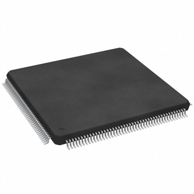


 工商网监
湘ICP备2023018690号
工商网监
湘ICP备2023018690号
