Is Now Part of
To learn more about ON Semiconductor, please visit our website at
www.onsemi.com
Please note: As part of the Fairchild Semiconductor integration, some of the Fairchild orderable part numbers
will need to change in order to meet ON Semiconductor’s system requirements. Since the ON Semiconductor
product management systems do not have the ability to manage part nomenclature that utilizes an underscore
(_), the underscore (_) in the Fairchild part numbers will be changed to a dash (-). This document may contain
device numbers with an underscore (_). Please check the ON Semiconductor website to verify the updated
device numbers. The most current and up-to-date ordering information can be found at www.onsemi.com. Please
email any questions regarding the system integration to Fairchild_questions@onsemi.com.
ON Semiconductor and the ON Semiconductor logo are trademarks of Semiconductor Components Industries, LLC dba ON Semiconductor or its subsidiaries in the United States and/or other countries. ON Semiconductor owns the rights to a number
of patents, trademarks, copyrights, trade secrets, and other intellectual property. A listing of ON Semiconductor’s product/patent coverage may be accessed at www.onsemi.com/site/pdf/Patent-Marking.pdf. ON Semiconductor reserves the right
to make changes without further notice to any products herein. ON Semiconductor makes no warranty, representation or guarantee regarding the suitability of its products for any particular purpose, nor does ON Semiconductor assume any liability
arising out of the application or use of any product or circuit, and specifically disclaims any and all liability, including without limitation special, consequential or incidental damages. Buyer is responsible for its products and applications using ON
Semiconductor products, including compliance with all laws, regulations and safety requirements or standards, regardless of any support or applications information provided by ON Semiconductor. “Typical” parameters which may be provided in ON
Semiconductor data sheets and/or specifications can and do vary in different applications and actual performance may vary over time. All operating parameters, including “Typicals” must be validated for each customer application by customer’s
technical experts. ON Semiconductor does not convey any license under its patent rights nor the rights of others. ON Semiconductor products are not designed, intended, or authorized for use as a critical component in life support systems or any FDA
Class 3 medical devices or medical devices with a same or similar classification in a foreign jurisdiction or any devices intended for implantation in the human body. Should Buyer purchase or use ON Semiconductor products for any such unintended
or unauthorized application, Buyer shall indemnify and hold ON Semiconductor and its officers, employees, subsidiaries, affiliates, and distributors harmless against all claims, costs, damages, and expenses, and reasonable attorney fees arising out
of, directly or indirectly, any claim of personal injury or death associated with such unintended or unauthorized use, even if such claim alleges that ON Semiconductor was negligent regarding the design or manufacture of the part. ON Semiconductor
is an Equal Opportunity/Affirmative Action Employer. This literature is subject to all applicable copyright laws and is not for resale in any manner.
�1N4728A - 1N4758A
Zener Diodes
Tolerance = 5%
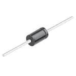
DO-41 Glass case
COLOR BAND DENOTES CATHODE
Absolute Maximum Ratings *
Symbol
PD
TJ, TSTG
Ta = 25°C unless otherwise noted
Value
Units
Power Dissipation
@ TL 50C, Lead Length = 3/8”
Parameter
1.0
W
Derate above 50C
6.67
mW/C
-65 to +200
C
Operating and Storage Temperature Range
* These ratings are limiting values above which the serviceability of the diode may be impaired.
Electrical Characteristics
Ta = 25°C unless otherwise noted
VZ (V) @ IZ (Note 1)
Device
Max. Zener Impedance
Test Current
IZ (mA)
ZZ @ IZ ZZK @
IZK
Max.
()
IZK () (mA)
VR
(V)
IZSM (mA) (Note 2)
1
1
1
1
1
100
100
50
10
10
1
1
1
1
1
1380
1260
1190
1070
970
550
600
700
700
700
1
1
1
1
0.5
10
10
10
10
10
1
2
3
4
5
890
810
730
660
605
700
700
700
700
700
0.5
0.5
0.25
0.25
0.25
10
10
10
5
5
6
7
7.6
8.4
9.1
550
500
454
414
380
Typ.
1N4728A
1N4729A
1N4730A
1N4731A
1N4732A
3.135
3.42
3.705
4.085
4.465
3.3
3.6
3.9
4.3
4.7
3.465
3.78
4.095
4.515
4.935
76
69
64
58
53
10
10
9
9
8
400
400
400
400
500
1N4733A
1N4734A
1N4735A
1N4736A
1N4737A
4.845
5.32
5.89
6.46
7.125
5.1
5.6
6.2
6.8
7.5
5.355
5.88
6.51
7.14
7.875
49
45
41
37
34
7
5
2
3.5
4
1N4738A
1N4739A
1N4740A
1N4741A
1N4742A
7.79
8.645
9.5
10.45
11.4
8.2
9.1
10
11
12
8.61
9.555
10.5
11.55
12.6
31
28
25
23
21
4.5
5
7
8
9
© 2009 Fairchild Semiconductor Corporation
Non-Repetitive
Peak Reverse
Current
IR
(A)
Min.
1N4728A - 1N4758A Rev. H3
Leakage
Current
www.fairchildsemi.com
1
1N4728A - 1N4758A — Zener Diodes
April 2009
�Device
Max. Zener Impedance
Test Current
IZ (mA)
ZZ @ IZ ZZK @
Max.
()
IZK ()
Leakage
Current
Non-Repetitive
Peak Reverse
Current
IZK
(mA)
IR
(A)
VR
(V)
IZSM (mA) (Note 2)
700
700
700
750
750
0.25
0.25
0.25
0.25
0.25
5
5
5
5
5
9.9
11.4
12.2
13.7
15.2
344
304
285
250
225
23
25
35
40
45
750
750
750
1000
1000
0.25
0.25
0.25
0.25
0.25
5
5
5
5
5
16.7
18.2
20.6
22.8
25.1
205
190
170
150
135
7
6.5
6
5.5
5
50
60
70
80
95
1000
1000
1500
1500
1500
0.25
0.25
0.25
0.25
0.25
5
5
5
5
5
27.4
29.7
32.7
35.8
38.8
125
115
110
95
90
4.5
110
2000
0.25
5
42.6
80
Min.
Typ.
1N4743A
1N4744A
1N4745A
1N4746A
1N4747A
12.35
14.25
15.2
17.1
19
13
15
16
18
20
13.65
15.75
16.8
18.9
21
19
17
15.5
14
12.5
10
14
16
20
22
1N4748A
1N4749A
1N4750A
1N4751A
1N4752A
20.9
22.8
25.65
28.5
31.35
22
24
27
30
33
23.1
25.2
28.35
31.5
34.65
11.5
10.5
9.5
8.5
7.5
1N4753A
1N4754A
1N4755A
1N4756A
1N4757A
34.2
37.05
40.85
44.65
48.45
36
39
43
47
51
37.8
40.95
45.15
49.35
53.55
1N4758A
53.2
56
58.8
Notes:
1. Zener Voltage (VZ)
The zener voltage is measured with the device junction in the thermal equilibrium at the lead temperature (TL) at 30C ± 1C and 3/8” lead length.
2. 2 Square wave Reverse Surge at 8.3 msec soak time.
Top Mark Information
Line 1
Line 2
Line 3
Line 4
Line 5
1N4728A
1N4729A
1N4730A
1N4731A
1N4732A
Device
LOGO
LOGO
LOGO
LOGO
LOGO
47
47
47
47
47
28
29
30
31
32
A
A
A
A
A
XY
XY
XY
XY
XY
1N4733A
1N4734A
1N4735A
1N4736A
1N4737A
LOGO
LOGO
LOGO
LOGO
LOGO
47
47
47
47
47
33
34
35
36
37
A
A
A
A
A
XY
XY
XY
XY
XY
1N4738A
1N4739A
1N4740A
1N4741A
1N4742A
LOGO
LOGO
LOGO
LOGO
LOGO
47
47
47
47
47
38
39
40
41
42
A
A
A
A
A
XY
XY
XY
XY
XY
1N4743A
1N4744A
1N4745A
1N4746A
1N4747A
LOGO
LOGO
LOGO
LOGO
LOGO
47
47
47
47
47
43
44
45
46
47
A
A
A
A
A
XY
XY
XY
XY
XY
1N4748A
1N4749A
1N4750A
1N4751A
1N4752A
LOGO
LOGO
LOGO
LOGO
LOGO
47
47
47
47
47
48
49
50
51
52
A
A
A
A
A
XY
XY
XY
XY
XY
1N4753A
1N4754A
1N4755A
1N4756A
1N4757A
LOGO
LOGO
LOGO
LOGO
LOGO
47
47
47
47
47
53
54
55
56
57
A
A
A
A
A
XY
XY
XY
XY
XY
1N4758A
LOGO
47
58
A
XY
© 2009 Fairchild Semiconductor Corporation
1N4728A - 1N4758A Rev. H3
www.fairchildsemi.com
2
1N4728A - 1N4758A — Zener Diodes
VZ (V) @ IZ (Note 1)
�1st line: F - Fairchild Logo
F
2nd line: Device Name - 3rd to 4th characters of device name for 1Nxx series
or 4th to 6th characters for BZXyy series
47
3rd line: Device Name - 5th to 6th characters of device name for 1Nxx series
or Voltage rating for BZXyy series
36
A
4th line: Device Name - 7th to 8th characters of device name for 1Nxx series
or Large Die identification only for BZXyy series
5th line: Date Code - Two Digit - Six Weeks Date Code
XY
F
General Requirements:
1.0 Cathode Band
2.0 First Line: F - Fairchild Logo
3.0 Second Line: Device name - For 1Nxx series: 3rd to 4th characters of the device name.
For BZxx series: 4th to 6th characters of the device name.
4.0 Third Line: Device name - For 1Nxx series: 5th to 6th characters of the device name.
For BZXyy series: Voltage rating
5.0 Third Line: Device name - For 1Nxx series: 7th to 8th characters of the device name.
(the 8th character is the large die identification)
For BZXyy series: Large Die Identification character
6.0 Fourth Line: Date Code - Two Digit - Six Weeks Date Code
Where: X represents the last digit of the calendar year
Y represents the Six weeks numeric code
7.0 Devices shall be marked as required in the device specification (PID or FSC Test Spec).
8.0 Maximum no. of marking lines: 5
9.0 Maximum no. of digits per line: 3
10.0 FSC logo must be 20 % taller than the alphanumeric marking and should occupy the 2 characters of the specified line.
11.0 Marking Font: Arial (Except FSC Logo)
12.0 First character of each marking line must be aligned vertically.
13.0 All device markings must be based on Fairchild device specification.
© 2009 Fairchild Semiconductor Corporation
1N4728A - 1N4758A Rev. H3
www.fairchildsemi.com
3
1N4728A - 1N4758A — Zener Diodes
Top Mark Information (Continued)
��ON Semiconductor and
are trademarks of Semiconductor Components Industries, LLC dba ON Semiconductor or its subsidiaries in the United States and/or other countries.
ON Semiconductor owns the rights to a number of patents, trademarks, copyrights, trade secrets, and other intellectual property. A listing of ON Semiconductor’s product/patent
coverage may be accessed at www.onsemi.com/site/pdf/Patent−Marking.pdf. ON Semiconductor reserves the right to make changes without further notice to any products herein.
ON Semiconductor makes no warranty, representation or guarantee regarding the suitability of its products for any particular purpose, nor does ON Semiconductor assume any liability
arising out of the application or use of any product or circuit, and specifically disclaims any and all liability, including without limitation special, consequential or incidental damages.
Buyer is responsible for its products and applications using ON Semiconductor products, including compliance with all laws, regulations and safety requirements or standards,
regardless of any support or applications information provided by ON Semiconductor. “Typical” parameters which may be provided in ON Semiconductor data sheets and/or
specifications can and do vary in different applications and actual performance may vary over time. All operating parameters, including “Typicals” must be validated for each customer
application by customer’s technical experts. ON Semiconductor does not convey any license under its patent rights nor the rights of others. ON Semiconductor products are not
designed, intended, or authorized for use as a critical component in life support systems or any FDA Class 3 medical devices or medical devices with a same or similar classification
in a foreign jurisdiction or any devices intended for implantation in the human body. Should Buyer purchase or use ON Semiconductor products for any such unintended or unauthorized
application, Buyer shall indemnify and hold ON Semiconductor and its officers, employees, subsidiaries, affiliates, and distributors harmless against all claims, costs, damages, and
expenses, and reasonable attorney fees arising out of, directly or indirectly, any claim of personal injury or death associated with such unintended or unauthorized use, even if such
claim alleges that ON Semiconductor was negligent regarding the design or manufacture of the part. ON Semiconductor is an Equal Opportunity/Affirmative Action Employer. This
literature is subject to all applicable copyright laws and is not for resale in any manner.
PUBLICATION ORDERING INFORMATION
LITERATURE FULFILLMENT:
Literature Distribution Center for ON Semiconductor
19521 E. 32nd Pkwy, Aurora, Colorado 80011 USA
Phone: 303−675−2175 or 800−344−3860 Toll Free USA/Canada
Fax: 303−675−2176 or 800−344−3867 Toll Free USA/Canada
Email: orderlit@onsemi.com
© Semiconductor Components Industries, LLC
N. American Technical Support: 800−282−9855 Toll Free
USA/Canada
Europe, Middle East and Africa Technical Support:
Phone: 421 33 790 2910
Japan Customer Focus Center
Phone: 81−3−5817−1050
www.onsemi.com
1
ON Semiconductor Website: www.onsemi.com
Order Literature: http://www.onsemi.com/orderlit
For additional information, please contact your local
Sales Representative
www.onsemi.com
�


 工商网监
湘ICP备2023018690号
工商网监
湘ICP备2023018690号

